Article

Automatic Reclaimed Wafer Classification Using Deep Learning Neural Networks

1
Business School, University of Shanghai for Science and Technology, Shanghai 200093, China
2
Department of Industrial Engineering and Management, Chaoyang University of Technology, Taichung 41349, Taiwan
3
Department of Industrial Engineering and Management, National Taipei University of Technology, Taipei 10632, Taiwan
*
Author to whom correspondence should be addressed.
Symmetry 2020, 12(5), 705; https://doi.org/10.3390/sym12050705
Submission received: 29 February 2020 / Revised: 29 March 2020 / Accepted: 15 April 2020 / Published: 2 May 2020

Abstract

:
Silicon wafer is the most crucial material in the semiconductor manufacturing industry. Owing to limited resources, the reclamation of monitor and dummy wafers for reuse can dramatically lower the cost, and become a competitive edge in this industry. However, defects such as void, scratches, particles, and contamination are found on the surfaces of the reclaimed wafers. Most of the reclaimed wafers with the asymmetric distribution of the defects, known as the “good (G)” reclaimed wafers, can be re-polished if their defects are not irreversible and if their thicknesses are sufficient for re-polishing. Currently, the “no good (NG)” reclaimed wafers must be first screened by experienced human inspectors to determine their re-usability through defect mapping. This screening task is tedious, time-consuming, and unreliable. This study presents a deep-learning-based reclaimed wafers defect classification approach. Three neural networks, multilayer perceptron (MLP), convolutional neural network (CNN) and Residual Network (ResNet), are adopted and compared for classification. These networks analyze the pattern of defect mapping and determine not only the reclaimed wafers are suitable for re-polishing but also where the defect categories belong. The open source TensorFlow library was used to train the MLP, CNN, and ResNet networks using collected wafer images as input data. Based on the experimental results, we found that the system applying CNN networks with a proper design of kernels and structures gave fast and superior performance in identifying defective wafers owing to its deep learning capability, and the ResNet averagely exhibited excellent accuracy, while the large-scale MLP networks also acquired good results with proper network structures.

1. Introduction

Wafers are the most essential semiconductor materials, and therefore is considered to be a major resource in the semiconductor industry. Wafers can be divided into two categories: prime wafers and test wafers, which are shown in Figure 1. The test wafers are further classified into two types: control (monitor) wafers and dummy wafers. The prime wafers are used to manufacture ICs, and the test wafers are mainly used to monitor parameters and maintain machines during the manufacturing process. However, the prime wafer has been produced as IC chips, and only test wafers can be reclaimed [1]. As the wafer is a limited and valuable resource, it is desirable that they are recycled or reclaimed, as this can significantly cut expenses in the manufacturing industry. In other words, greater reusability results in higher profit, and therefore higher competence, among the IC foundries.
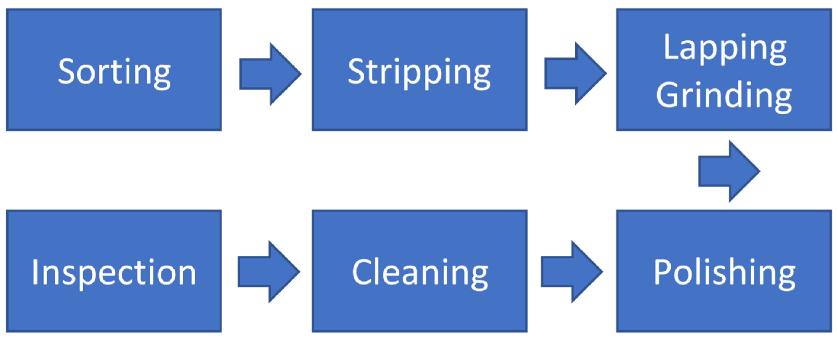
The reclaiming process is as depicted in Figure 2. The key processing steps include sorting, stripping, lapping and grinding, polishing, cleaning, and inspection [2]. Because not all processed test wafers can be reclaimed, a screening process should be adopted to classify the test wafers into two types: ‘good (G)’ and ‘no good (NG)’. For the G type, the wafers can be re-polished and reused in the manufacturing process. This type of re-polishable wafers can be further classified into nine categories (namely, T1-T9) based on their mappings due to different root causes. For the NG type, the wafers cannot be polished, and hence are scrapped. Among these steps, the inspection step, wherein the reusability of reclaimed wafers is determined, is considered to be the most critical task and, generally, a considerable amount of labor and time is spent on it. Therefore, an artificial intelligence-based method is herein proposed to classify the defective reclaimed wafer, to reduce both labor and time, increase profit, and enhance the competitiveness of manufacturing factories.
The remainder of this paper is arranged as follows. In Section 2, the automated visual inspection and related topics are introduced. Section 3 describes the research method. A number of experiments are carried out to validate and compare the performance of MLP, CNN and ResNet in Section 4. Discussion and conclusions are given in Section 5.

2. Review

Automated visual inspection (AVI) is an image-processing technique for production automation and quality control. It has been widely applied in the production of manufacturing industries, such as for electrical and mechanical parts, electronic, vehicles, textile, and the food industry. In the semiconductor industry, Huang and Pan [3] made a clear investigation into the applications of AVI. AVI can be used to solve the quality problems instead of an engineer, who requires time for well-training but has an inspection quality which is unreliable and inconsistent. Besides, the labor cost is a main consideration factor for manufacturers and the working hours of a quality engineer are relatively long. In practice, using a circuit probe test to detect the dies of wafer is the main approach to represent the distribution of wafer defects into bin maps, the so-called wafer beam map (WBM). Most companies hire experienced and highly paid human inspectors to analyze WBM [4], and this method uses a lot of labor and time resources. Therefore, many different data mining techniques have been proposed and applied in order to effectively identify the possible re-polishing candidate.
Hsu and Chien [5] developed a hybrid data mining approach which combined adaptive resonance theory (ART), neural networks and spatial statistics to quickly extract patterns from WBM. Liu and Chien [4] proposed a system which integrates the geometric information of distributed WBM, and uses the adaptive resonance theory, the moment invariant and the cellular neural network for the classification problem. In their paper, the proposed system recognized specific failure patterns efficiently, and traced the root causes as well. Li and Tsai [6] proposed a machine vision-based method to automatically detect the saw-mark defects on the surface of solar wafers. First, they removed the multi-grain background of a solar wafer image by using Fourier image reconstruction, and then used Hough transform to detect low-contrast saw-mark defects. Li and Tsai [7] used wavelet transform techniques to detect the defects of multi-crystalline solar wafer, such as saw-mark, contamination, and fingerprint. Sun et al. [8] introduced a machine vision-based inspection approach that uses a heuristic method to facilitate solving the maximum inscribed circle (MIC) problem. The proposed method incorporates the particle swarm optimization (PSO) with Hooke–Jeeves pattern search (H-J PS) to achieve fast convergence and quality solution for silicon wafer inspection. Wang [9] developed a spatial defect diagnosis system to identify the defects on the wafer surface. The proposed system eliminated the noise of wafer map by using entropy fuzzy means, and then used a decision tree to classify the defects based on the features of clusters. Chang et al. [10] classified the wafers into four clusters by first removing noises with median filter, and then clustering the defects based on the spatial information of blocks. Shankar and Zhong [11] proposed a template-based vision system to inspect the wafer die surfaces. Su and Tong [12] introduced a neural-network-based method to monitor the clustered defects in integrated circuit fabrication. This method effectively reduced the warning errors caused by clustered defects. Su et al. [13] used three kinds of neural networks, which are backpropagation (BPN), radial basis function (RBFN), and learning vector quantization (LVQ) networks, in post-sawing semiconductor wafer detection. Chang et al. [14] proposed an inspection system, which automatically recognizes the defective patterns. Their system used the Radial basis function neural network (RBFN) that successfully identified the defective dies on the images of LED wafers. Ooi et al. [15] used Invariant Moment and Polar Fourier Transformation to obtain invariant features of surface defects, and then a top-down induction decision tree and Bayesian classifier was applied to classify different product types. Finally, their system adopted the ADTree classifier to achieve a classification accuracy of up to 95%.
Multilayer Perceptron (MLP) used to be the best classifier to solve the classification problem. However, the performance of the MLP network is limited by the property of gradient explosion and diminishing, and the MLP network has been gradually replaced by deep learning models [16]. Convolutional Neural Networks (CNN) are one of the most popular architectures in deep learning, and achieve the best published results on benchmarks for object classification (such as NORB and CIFAR10) and handwritten digit recognition (MNIST). CNNs are hierarchical neural networks and have been successfully used for image classification [17,18], image retrieval [19,20], object detection [21,22], semantic segmentation [23,24], etc. Ciresan et al. [25] present a fast, fully parameterizable GPU implementation of CNN variants. The feature extractors are learned in a supervised way without being carefully designed or pre-wired. Among the deep learning networks, ResNet is the one of the most popularly used networks. This network overcomes the gradient vanishing problem by stacking identity shortcut and skipping compresses layers to pass the residual into deep layers, so that quick and good results can be easily reached during learning [26].
According to the above researches, there is much research related to the prime wafers. Very limited references related to the reclaimed wafers are discussed, except some which describe the cleaning techniques of reclaimed wafers [27,28]. The main purpose of the defect inspection of prime wafers is to find out the circuit flaw, while the purpose of the defect inspection of test wafers is to find out which wafers can be reclaimed. There is a fundamental difference between the defect inspection of prime wafers and test wafers. In order to solve this problem, we used SVM to classify two types of reclaimed wafers (type G and type NG) with invariant features and derived a fair classification of around 80% accuracy in our previous research [29]. The experiment result showed that the classification accuracy was obviously affected by the inappropriate features. Then, backpropagation neural networks with one hidden layer were used to classify reclaimed wafers (type G and type NG) with self-extracted features [30]. Furthermore, few basic structures of CNNs were applied to classify the reclaimed wafers as a pilot study [31]. This study shows that CNN could extract prominent key features by convolutional layer.

3. Research Method

The objective of this study is to build up neural networks, MLP, CNN, and ResNet, to classify not only the Good and No-Good reclaimed wafers but also their categories of defects, such that the human inspector can be relieved from the laborious and tedious work, and the causes of defects can be traced.

3.1. Ten Typical Defective Maps in Reclaimed Wafers

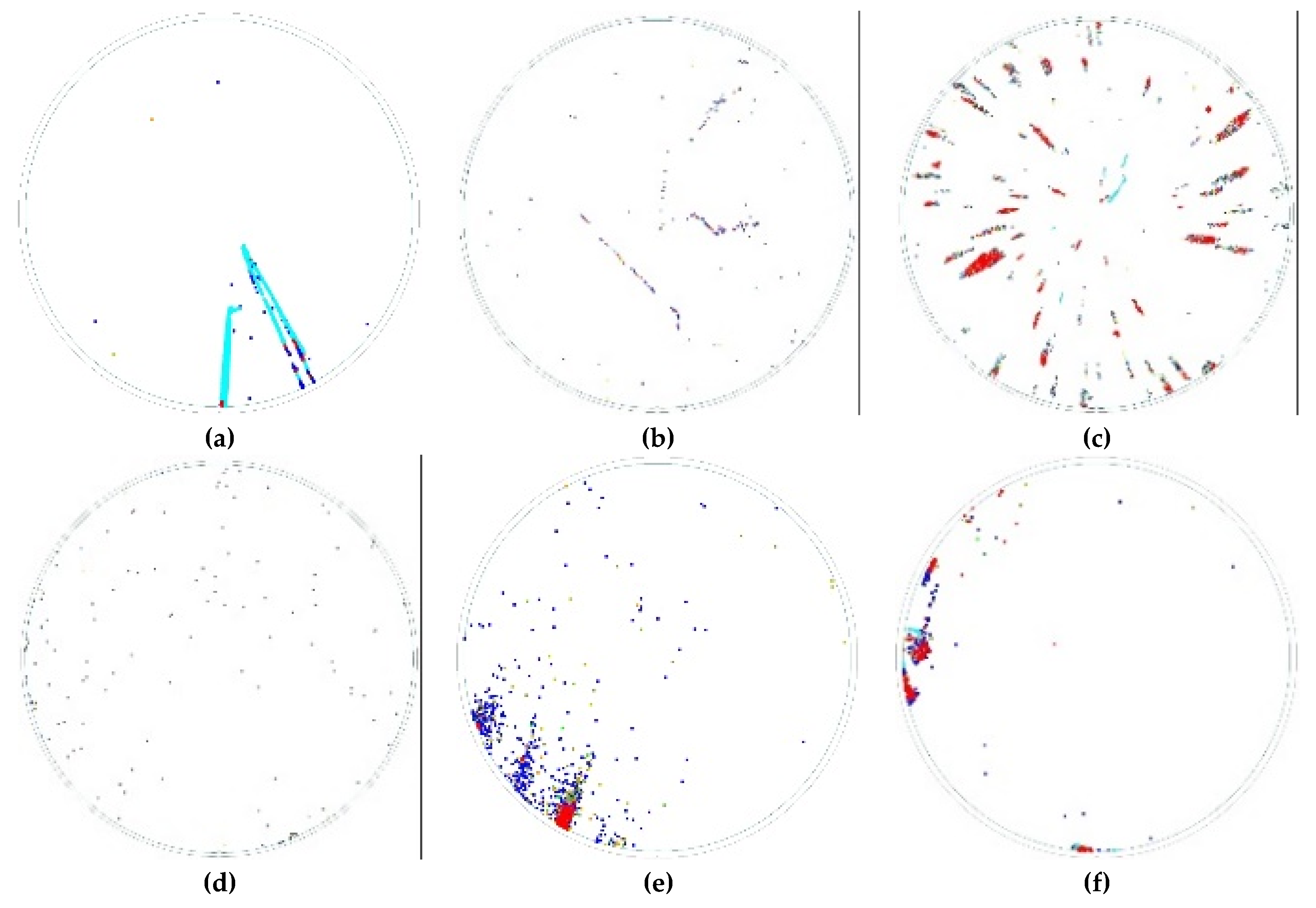
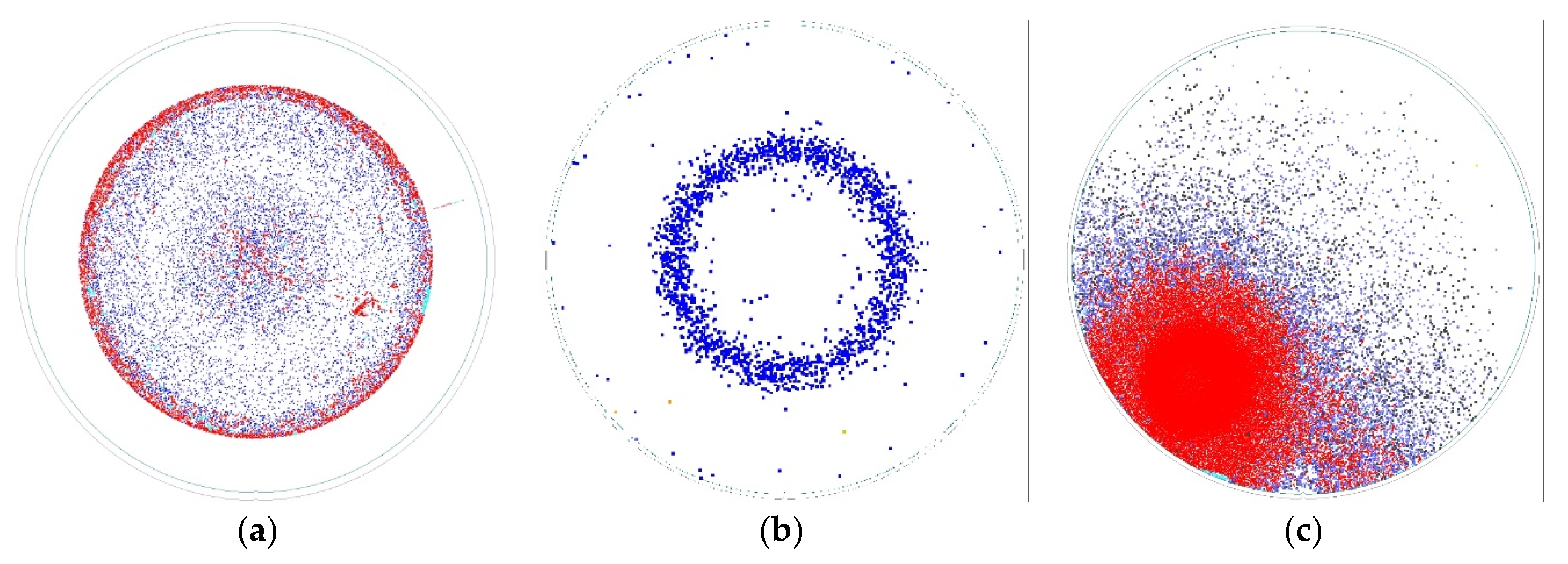
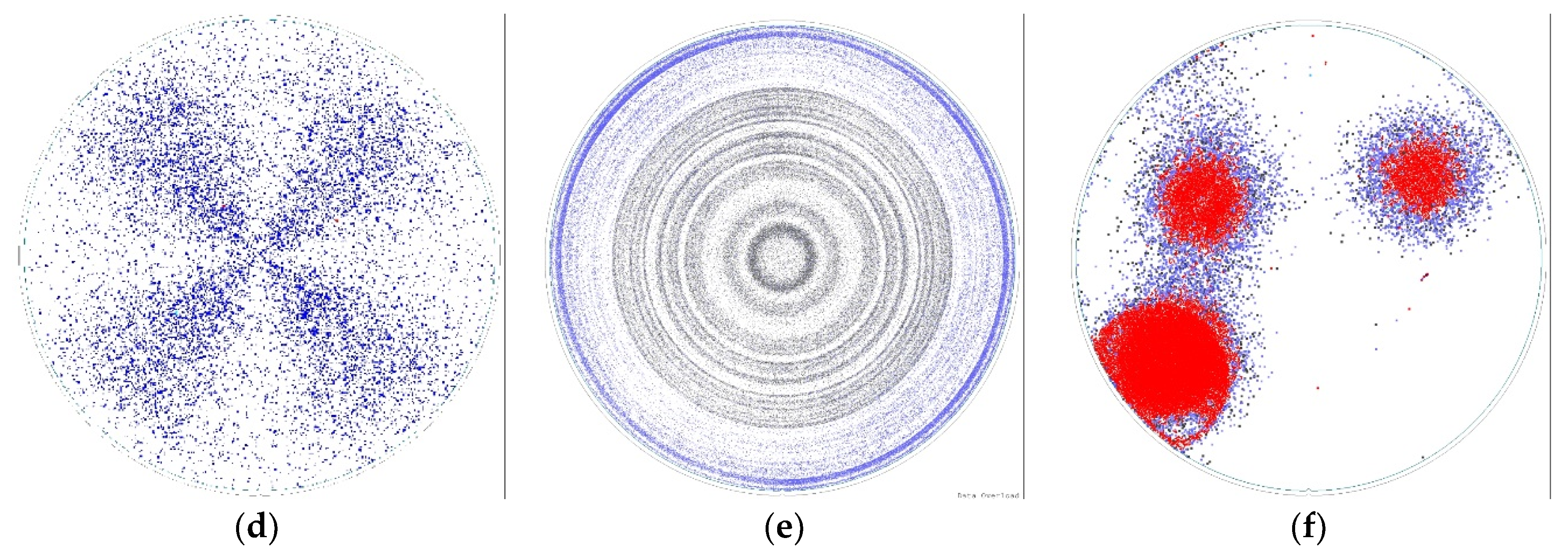
The defective maps in reclaimed wafers are classified into ten categories based on the color and distribution of the defects. The characteristics and causes of ten typical defective maps, as shown in Figure 3 and Figure 4, are described as follows. In Figure 3, these nine categories are re-polishable Good wafers. Conversely, in Figure 4, other wafers are No-Good wafers.
(1)
Surface with line watermarks: there are residues on the surface of reclaimed wafers caused by the cleaning and rotary drying process. The representative pattern is shown in Figure 3a;
(2)
Surface with scratches: there are scratches on the surface of reclaimed wafers caused by the manufacturing process such as grinding. The representative pattern is shown in Figure 3b;
(3)
Surface with scattered watermarks: there are radiance defective marks on the surface of reclaimed wafers caused by the cleaning and rotary drying process. Figure 3c shows the representative pattern;
(4)
Surface with over-etched spot: there are blue and green points on the surface of reclaimed wafers caused by the over-etching. The representative pattern is shown in Figure 3d;
(5)
Surface with water jet: there are parallel straight defective marks on the surface of reclaimed wafers caused by an abnormal cleaning process. Figure 3e shows the representative pattern;
(6)
Surface with clustered watermarks: there are marginal defective watermarks on the surface of reclaimed wafers caused by the damaged parts of the cleaning machine. The representative pattern is shown in Figure 3f;
(7)
Surface with half-sided watermarks: the cause of formation is the same as (6) above, but the defective characteristics are different. The representative pattern is shown in Figure 3g;
(8)
Surface with Eridite residuals: there are residues of polishing liquid on the surface of reclaimed wafers caused by the abnormal machine. The representative pattern is shown in Figure 3h;
(9)
Surface with banded particles: there are ribbon/banding defective marks on the surface of reclaimed wafers caused by the damaged parts of the cleaning machine. The representative pattern is shown in Figure 3i;
(10)
Crystal growth defect: this kind of reclaimed wafers can no longer be used in the manufacturing process due to the abnormal material. If a wafer cannot be classified into one of the first nine categories, this wafer will be recognized as a No-Good wafer. Therefore, the total number of categories of the No-Good wafers cannot be counted clearly. Figure 4 shows six example images of the No-Good wafers.
In the traditional method, the human inspector tries to find the good wafers according to their experiences. However, the defects between some categories have similar distribution and clustering characteristics. The human inspector often has inconsistent classification between over-etched spot, scratches, Eridite residuals, and Crystal growth defect. The traditional heuristic method, such as SVM, produced a fair accuracy of classification with pre-defined invariant features such as color and hu moments [29]. In addition, the size, location, shape and direction of defects of reclaimed wafers are different. Therefore, how to retrieve and classify defective maps effectively becomes an important issue.

3.2. Proposed Method

The proposed process of research, including data acquisition, data transformation, image preprocessing, network structure determination, and network validation and evaluation, is shown as Figure 5. After network determination, the deep learning networks are validated and evaluated.

3.2.1. Data Acquisition

The 3D information of the reclaimed wafer surfaces is acquired by the automatic optical inspection (AOI) instrument (called G-sorter). The derived information includes the position of particles, the geometry, the flatness, and so forth. However, the amount of derived data is huge and presented into digital data which cannot be directly inspected by a human inspector.

3.2.2. Data Transformation

The purpose of the data transformation is to convert the digital data into a graphical map, as described in Section 3.1. Therefore, the human inspector can classify the reclaimed wafers into G and NG types based on the color and distribution of the defect particles. The different colors represent the various heights of the position, and the clustered point characteristics of defects such as scratches, watermarks, pits and spots.

3.2.3. Image Preprocessing

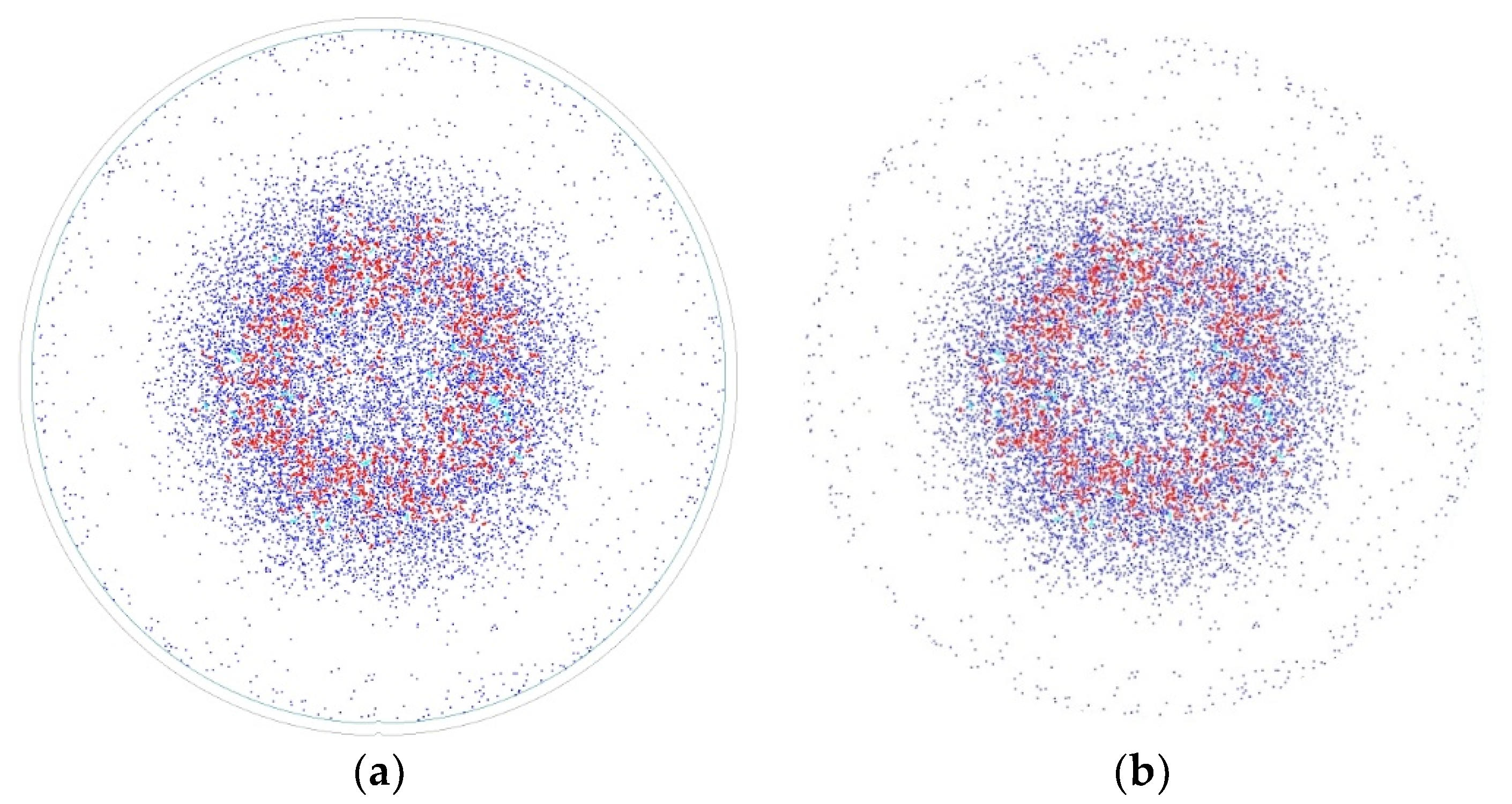
The purpose of the image preprocessing for reclaim wafer is to remove the irrelevant information and resize the image into feasible size for further processing. Figure 6a,b shows the edge of the reclaim wafer image and the boundary of the image, which may be digitized differently during data acquisition and are removed before further processing. Then, these color feature maps are resized into a feasible size for training due to time and hardware GPU memory limitations. All ten categories of defects are labelled into Type 1 (T1) to Type 10 (T10), as shown in Table 1. Due to the different causes and the different happening frequencies of defects, the number of defects collected is limited and imbalanced.
In this paper, we used OpenCV to conduct the preprocessing. The algorithm of image preprocessing is described as the following steps. Figure 7 shows the images before and after preprocessing.
  • Step 1: Read in the image;
  • Step 2: Resize the image into predefined size (e.g., 134 by 134);
  • Step 3: Crop the image by three to certain pixels width (e.g., Width = 3);
  • Step 4: For a given pixel (r, c), if sqrt (r − center_r) × (r − center_r) + (c − center_c) × (c − center_c) > radius: pixel(r, c) = white (eg. radius = 60);
  • Step 5: Save the image.

3.2.4. Network Structure Determination

After image preprocessing, the network structure and the training parameter must be determined.

Reclaimed Wafer Classification Using MLP

Neural networks are trained via the backpropagation process, which relies on gradient descent, moving down the loss function to find the weights that minimize the loss function. The general MLP includes three types of layers—input layer, hidden layers, and output layer—and each layer contains a certain number of neurons. In the training process of an MLP network, a loss function, such as mean square errors (MSE), is constructed first, and then gradient vectors are obtained by the gradient descent optimization method (such as delta rule). Next, the weights and biases in the network are altered through batches of input images. After a pre-defined training epoch, the network converges to an acceptable loss value. However, when the network is large or deep, gradient explosion and vanishing often occur. Therefore, in recent years, the MSE loss function is replaced by the cross-entropy loss function, which is as shown in Equation (1):
L = 1 n i = 1 n [ t ln y + ( 1 t ) ln ( 1 y ) ]
where y is the predicting output value of the neural network, n is the number of training samples, and t is the target value. Another commonly used loss function is categorical cross entropy, as shown in Equation (2), which is mainly used to minimize the loss of categorical classification:
L = i = 1 n j = 1 c ( t i , j × log ( y i , j ) )
where n is the number of training samples; c is the number of classes, which is represented as one-hot notation of vector y. Instead of using sigmoid or tansig function, we used the rectified linear unit (ReLU), as shown in Figure 8, as a nonlinear activation function, which has better computation efficiency and fewer vanishing gradient problems compared to sigmoidal activation functions.
Softmax function is used in the output layer of the network, and this function directly converts the output result to a probability value. In this paper, we investigated the network structure through trial and error in order to avoid the overtraining phenomenon. In addition, due to the small amount of data, the stochastic gradient descent (SGD) method is selected as the learning algorithm. The reclaimed wafer image data are divided into batches for training, and different learning rates are tested at the same time.

Reclaimed Wafer Classification Using CNN

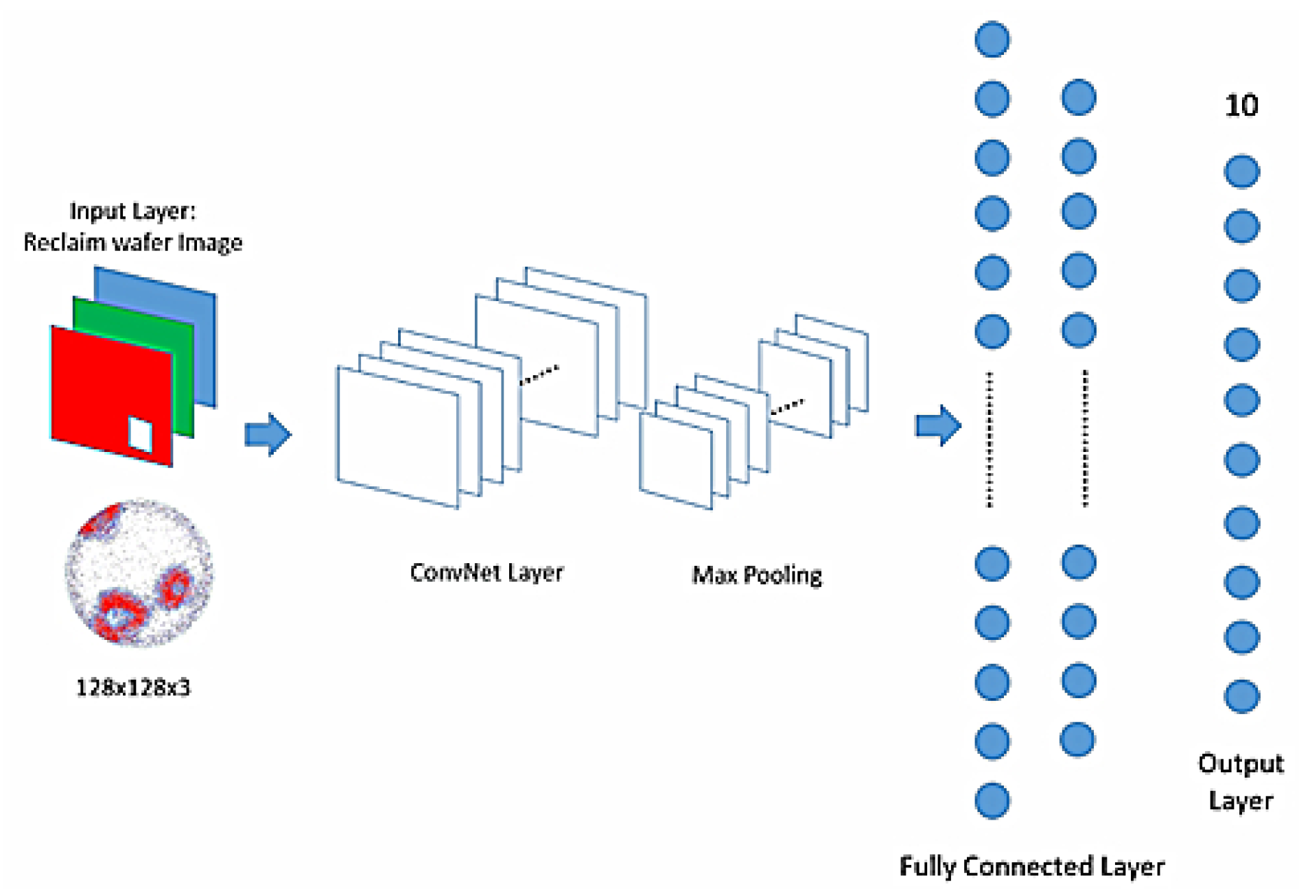
The typical structure of CNN is shown in Figure 9. It is composed of three different layers: the convolutional layer, pooling layer, and fully connected layer (FCL). The convolutional layer is designed to automatically extract the features from the input image and to generate feature maps. The pooling layer reduces the size of feature maps and retains the important features. The fully connected layer works like the traditional MLP to conduct the classification task based on the extracted feature maps. This study feeds the RGB reclaimed wafer image into the different structures of the CNN, and classifies them into ten different classes. Besides this, there are several parameters to be determined, such as input size, kernel (filter) dimensions, number of neurons in each layer, and the topology of the CNN [32].

Reclaimed Wafer Classification Using ResNets

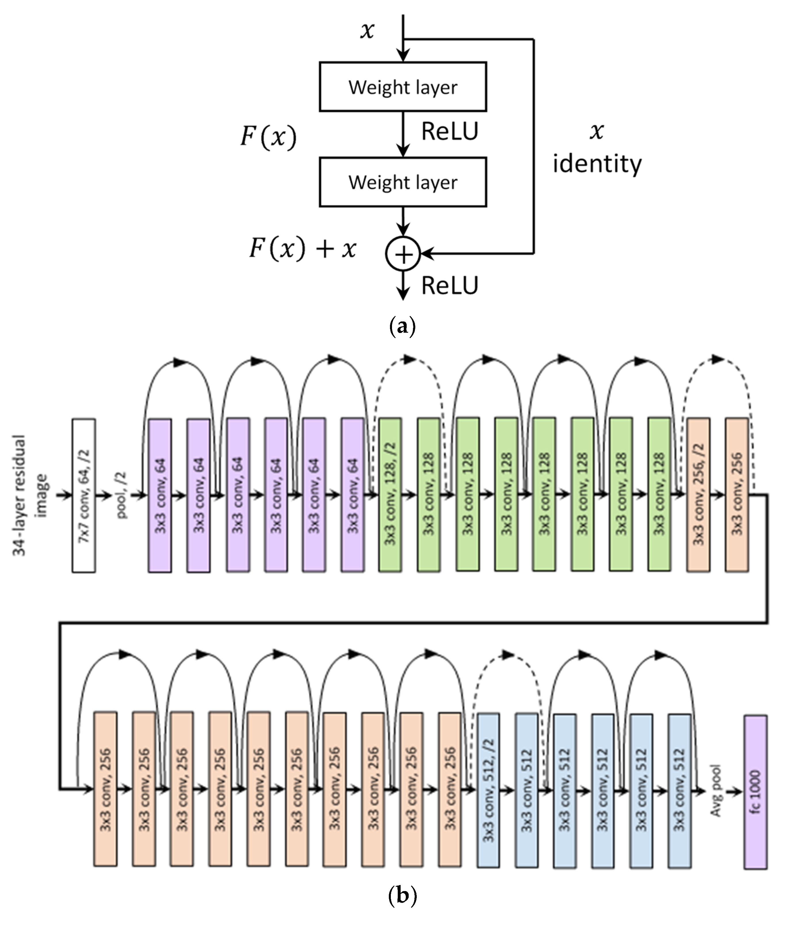
Residual Network (ResNet) is one the most popularly used deep neural network architecture which is designed to enable hundreds or thousands of convolutional layers without suffering the “gradient vanishing” problem. The ResNet uses “identity shortcut connections”, as shown in Figure 10a, to solve the gradient vanishing problem. Stacking up identity mappings and skipping over them, ResNet reuses the activations from previous layers. Skipping initially compresses the network into only a few layers, which enables faster learning. Then, when the network trains again, all layers are expanded and the “residual” parts of the network explore more of the feature space of the source image [33]. This is why ResNet can train with a large number of layers without degrading learning performance, while the CNN architectures had a drop off in the effectiveness of additional layers. The details of ResNet can be found in [26]. There are several popularly used ResNets with different depths of layers, such as ResNet 14, 34, 50, 101, and 152. Figure 10 shows the basic structure of ResNet 34.
The number of input neurons of ResNet is also determined by the image size of the reclaimed wafer, while the number of output neurons is determined by the number of classified classes, which is ten for the reclaimed wafer types. The categorical cross entropy loss function, as shown in Equation (2), is used as an objective function to minimize. The stochastic gradient descent (SGD), as the default training algorithm, is adopted as the learning algorithm with a mini-batch size. The training process is set to automatically stop training when the validation accuracy is less than the pre-determined objective accuracy, or there is no improvement in a certain amount of consecutive epochs.

4. Implementation

The proposed method was implemented in Python language under a Windows 10 platform. The MLP, CNN, and ResNet were implemented with Keras using Tensorflow as a backend [18]. A total of 2461 images, as shown in Table 1, were collected in the experiment. In order to make the training model robust and avoid overtraining, the data were augmented by flipping images vertically and horizontal so that the number of images is threefold. As mentioned previously, due to the different causes and happening frequencies of defects, the number of images in each category is uneven. Therefore, we balanced the data by rotating, flipping and duplicating the images according to the maximum data number of all types. In other words, we increased the data number of the NG type (T10) to 3183 by rotating and flipping the images. Then, we increased the data number of other types (T1 to T9) to close to the number of the NG type (T10) by rotating, flipping and duplicating the images. After balancing the data, we divided the data into the training and the validation datasets in an 80/20 ratio. Therefore, the total numbers of training and validation data were 26,571 and 6644 respectively. The mini-batch gradient decent method was adopted as the optimizer of the neural network. This method is mainly used to converge faster for a small dataset. Besides, due to the limitation of GPU capacity (memory and speed), the size of the training image cannot be too large, but must preserve the feature of mapping for classification. After trial-and-error, we chose 128 by 128. Therefore, the resolution of original image (1000 × 1000 pixels) was reduced to 128 × 128 and fed into the MLP, CNN and ResNet. After several trial and error experiments, the network structure and the training parameters were determined.

4.1. Experiment Results of MLP

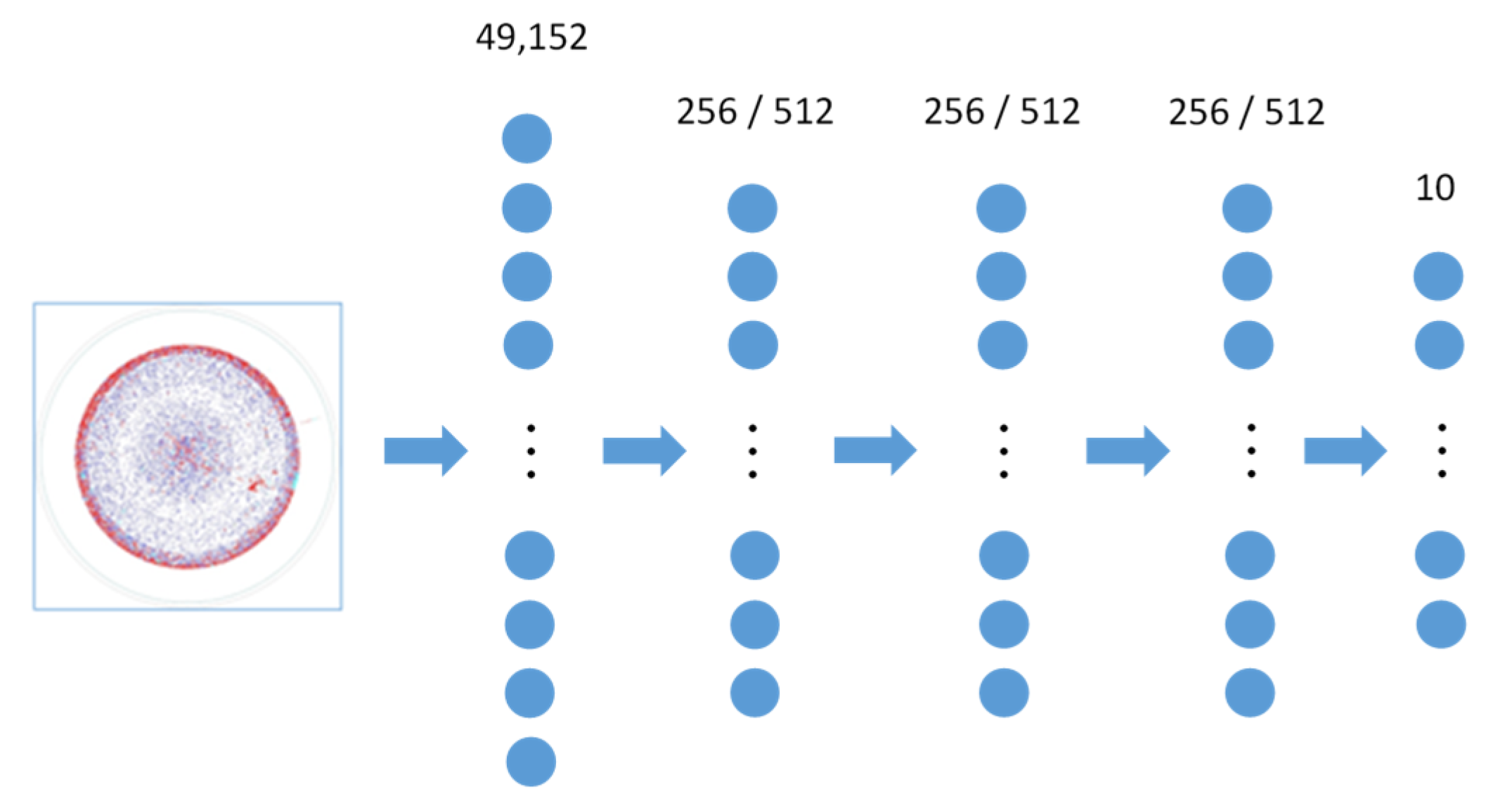
The large-scale MLP was constructed with the cross entropy as the loss function and ReLU function as the activation function. The number of input neurons of MLP was 49,152 (128 × 128 × 3), and the number of output neurons was set to ten, respectively. However, the number of hidden layers and its corresponding number of neurons were determined by a trial-and-error experiment. Figure 11 shows the structure of the MLP neural network used in this study.
The experiment of network training uses the incremental approach (increasing the number of hidden layer and neurons and the number of neurons in each layer from less to more both), so that the overtraining problem can be avoided. Besides, batch normalization is added to each layer instead of dropout, in order to avoid overtraining and to increase training speed. We divided all data into multiple mini batches (Batch Size = 100) and set the learning rate, decay, and momentum as 0.001, 1.000 × 10⁶, and 0.9, respectively. The total number of training iterations (epochs) was 300. The stopping criteria were set as the loss is less than 0.01, or the validation accuracy is greater than 0.9975, or no improvement in accuracy on consecutive 30 training iterations (patience stop criterion). Table 2 shows the parameters of the training process.
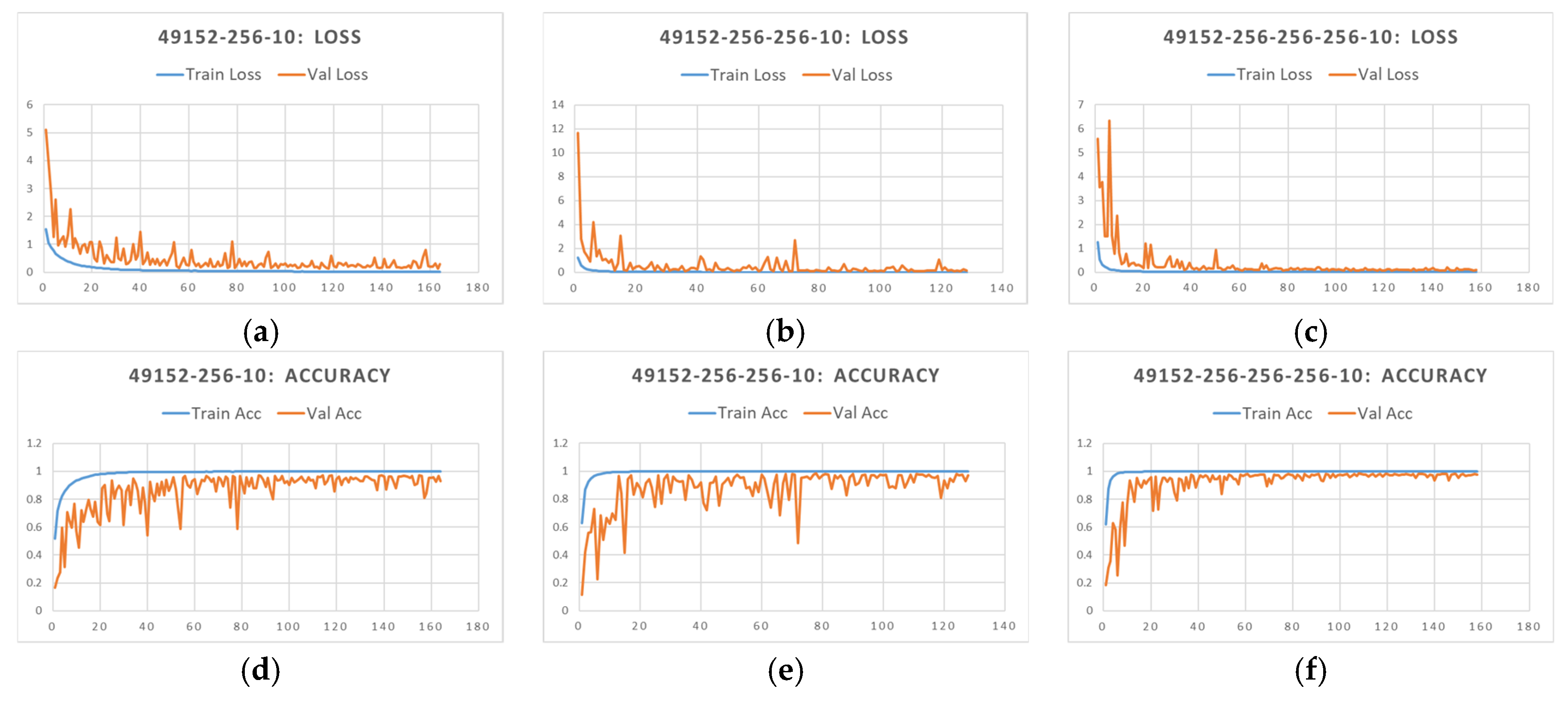
Figure 12 and Table 3 show the experiment results of three MLP structures with different hidden layers. In Figure 12a–c, the horizontal axis means the no. of epoch and the vertical axis means the cross-entropy loss value. In Figure 12d–f, the horizontal axis means the no. of epoch, and the Vertical axis means the accuracy. According to the results, we found that the convergence of networks with one or two hidden layers was more stable than the one with three hidden layers. However, the network with one hidden layer stopped training before full convergence because of the patience stopping criterion. The network with two and three hidden layers converged smoothly. The loss and accuracy of the testing and the validation data converged simultaneously, but the accuracy oscillation of the network with two hidden layers was larger than the network with three hidden layers. Besides, the loss value (0.0113) and the accuracy (0.9983) of 49152-256-256-256-10 network were fairly close to the preset stopping conditions. Therefore, the number of hidden layers of the MLP was determined as three.
After determination of the number of hidden layers, we investigated the proper number of hidden neurons. The experiment results are shown in Table 4. We found that the MLP with three hidden layers converged effectively with the loss values of each network of almost less than 0.0250, and the accuracy rate of training classification reached more than 99.80%. Among the networks, the 49152-512-256-512-10 structure had the better validation classification (0.9849). It is notable that the smaller loss value of the training data did not guarantee a higher recognition rate of the validation data.

4.2. Experiment Results of CNN

In this section, we present the experiment that finds a suitable CNN structure, based on [31], to classify the defects of reclaimed wafers. In our previous research [31], we set the fixed kernel size as three. According to the principle of CNN, fine features can be captured when the kernel size is small, while larger features can be captured when the kernel size is large, and the more complex the problem is, the more kernels and convolutional layers should be used. Therefore, we determined the structure of the CNN by trial-and-error, including the number of kernels, the size of the kernel, and the number of convolutional layers. The structure of the CNN is noted as model-C16(K5-ReLU-MP3)-C32(K3-ReLU-MP3)-F32(ReLU)-F10(SM), for example. Two types of convolutional layers (C) with 16 or 32 kernels (C16 or C32) were used with sizes of 3 or 5 (K3 or K5). ReLU were used to smooth the output in each layer. The size of max pooling was a given size of 3 × 3, and the stride of max pooling (MP3) is 3. Two layers of fully connected structure were adopted with 32 and 10 hidden neurons (F32 or F10). Softmax function (SM) was used at the last layer to convert the final prediction result into 0 to 9. A Batch Normalization layer was used at the end of the layer in order to avoid overtraining. The purpose of the SGD training algorithm is to minimize the cross entropy [34]. We tested different learning rates, and found that the CNN with the default parameter (learning rate = 0.01) can converge smoothly. As in the MLP experiment, the data were balanced and split into an 80/20 ratio for training and validation. The training iteration (number of epochs) was set as 300, which automatically stops when no improvement was made during the training process (Penitence = 30). A mini-batch training approach, which shuffling the training data and extract 100 data as a batch, was used to speed up the training process.
The input data was a colored image with RGB channel and 128 × 128 resolution, and the output data were ten classes. Figure 13 shows the structure of the CNN. Figure 14 and Table 5 show the experimental results of CNN with different numbers of convolutional layers. In Figure 14a–c, the horizontal axis means the no. of epoch and the vertical axis means the cross-entropy loss value. In Figure 14d–f, the horizontal axis means the no. of epoch and the vertical axis means the accuracy.
The experiment result shows that the CNN with two convolutional layers have a better convergence than with single convolutional layer. Besides, when the kernel size of convolutional layer 1 was 5, the network converged more effectively and quickly than the size was 3. In other words, the use of larger filters is more effective for defect detection of reclaimed wafers. The training procedure of CNN converged at about 100–130 epochs, so the number of stopping criterion was set to 150 epochs.
After determining the number of convolutional layers, we investigated the number of kernels, the size of kernel, and the number of neurons of fully connected layer. The experiment results are shown in Table 6.
According to the experiment results, the accuracies of these eight structures were all over 98%. Among these results of the No.1 to No.4 networks with kernel size 3, the No.2 network gave the best training and validation accuracy (0.9982; 0.9893). On the other hand, among the No.5 to No.8 networks, which adopted kernel size 5, the No.7 network reached the smaller validation loss value (0.0224) and the better validation accuracy (0.9975) among all eight results. Overall, the loss values and the accuracies of the No.5 to No.8 networks were better than those of the No.1 to No.4 respectively. For example, the loss values of the result No.5 (0.0096; 0.0332) were less than those of the result No.1 (0.0148; 0.0533), and the accuracy rates of the result No.5 (0.9982; 0.9936) were better than those of the result No.1 (0.9980; 0.9878). We note No.2 and No.7 as CNN_1 and CNN_2, respectively, for further comparison.

4.3. Experiment Results of ResNet

When using ResNet for classifying reclaimed wafers, the structures of ResNet 18, 34, 50, 101, and 152 were taken into consideration for implementation and comparison. The Keras ResNet model was coded based on [35]. We first chose ResNet 34 for a trial training with the prepared data such that the feasible training parameters including learning rate, momentum, number of epochs, batch size, were determined. The trial run shows that ResNet converged quickly with default learning rate so the number of training epochs was set as 50 arbitrarily. The mini-batch was also 100 as CNN experiments. The parameters of training algorithm SGD were set as default in Keras (same as CNN). The training process and results of ResNets are shown in Figure 15 and Table 7. In Figure 15a–e), in each upper figure, the horizontal axis means the no. of epoch and the vertical axis means the cross entropy loss value; in each lower figure, the horizontal axis means the no. of epoch and the Vertical axis means the accuracy.
As shown in Figure 15, all types of ResNet converged very fast at about epoch 5 to 10, and then kept moving forward for better solution. ResNet 18 took 50 s for an epoch, while ResNet 152 spent 185 s an epoch. All ResNets reached accuracy around 99.80% and 99.60% for classifying training and validation data, and those difference can be recognized as stochastic difference. Observing the training process, we found that spikes in loss or accuracy chart show the tendency of overtraining, but the loss or accuracy swung back to normal in the following epochs.

4.4. Comparison of MLP, CNN and ResNet

In this section, we compared the performance of the MLP, CNN and ResNet, based on the loss, accuracy, training time (speed) and the number of total weights and biases, as shown in Table 8. The best structure of the MLP network with the best performance was 16384-512-256-512-10, while the best structure of CNN_1 was C8(K3_ReLU_MP3)_C16(K3_ReLU_MP3)_F64(ReLU)_F10(SM), and the best structure of CNN_2 was C16(K5_ReLU_MP3)_C32(K3_ReLU_MP3)_F32(ReLU)_F10(SM). The ResNets performed approximately the same, so we chose the ResNet18, which used less parameters and about the same training time as MLP and CNN did, for comparison.
First of all, the MLP used 25,439,498 weights and biases. The number of CNN weights is less than MLP due to the local receptive field and the shared weights and biases. In addition, although K5 in CNN_2 used more weights, compared with F64 in CNN_1, the number of weights and biases generated by the full connection layer was much larger than those of F32 in CNN_2. Therefore, the amount of weights and biases in CNN_1 (235,978) was almost twice that in CNN_2 (119,514). ResNet 18 has the deepest structure, so used the most parameters. Secondly, during the training, ResNet 18 spent, on average, 51.1 secs, close to MLP’s 47.2 s, per epoch, while CNN_2 used the shortest time (30.2 secs). Because 64 hidden neurons of the full connection layer were used, the training time of CNN_1 was mainly spent on the operation of the full connection layer. It can be seen that the classification ability of CNN mainly lies in the number and size of kernels. On the other hand, the training of MLP was relatively difficult, although the training accuracy of MLP was close to that of CNN. The trial and error experiments of MLP had to be conducted more carefully in order to find appropriate weights, biases and network architecture. Training ResNet is rather straightforward, but requires more time per epoch due the size of networks. It is notable that ResNet converges very fast, so that the total training time is approximately same as the CNN training time. Before experiments, we expected that ResNet would obtain the best classification with its excellent structure design and fast convergence. However, a shallow CNN network structure classifies as excellently as a deep ResNet with an experimental design. With regard to the accuracy and loss, the structure with a high accuracy in training does not guarantee better validation accuracy, while the network trained with low loss does not promise higher accuracy. Therefore, the evaluation of network performance should still be based on the validation accuracy and the validation loss value in order to ensure the robustness of the future prediction.
In addition, Table 9 shows the confusion matrix of CNN_2 network. We find that the error classification mostly occurs between type 2 (surface with scratches) and type 4 (surface with over-etched spots). However, there are many similarities between these two types of defects, and the professional QC personnel sometimes hard to distinguish correctly.

5. Discussion and Conclusions

Silicon wafers are most important material in the semiconductor industry. To reduce the cost of manufacturing, the recovery of reclaimed wafers is an import issue. This study applied large-scale MLP, CNN, and ResNet to classify re-polishable wafers from the reclaimed ones. Full-scale images of reclaimed wafers were fed into the networks. Among the MLP models, the 16384-512-256-512-10 structure was found to achieve the best classification result, whereas, the structure of the CNN is noted as model-C16(K5_ReLU_MP3)_C32(K3_ReLU_MP3)_F32(ReLU)_F10(SM), and ResNets with different layers consistently and quickly reached good classification accuracy, but with large numbers of weights and biases. All these networks solved our problem effectively. Among them, the CNN model not only performed better than other models in terms of loss value and accuracy, but also required fewer parameters (weights and biases) and used less computation time for training and validation. Based on the experimental results, there are several findings in this study worth summarizing. Due to the structure of the MLP, CNN or ResNet model requiring huge input neurons, weights and biases, it takes a long training process to reach a feasible solution. However, with appropriate training parameters, loss function and activation function, the structure of MLP networks can be successfully utilized for image classification. Additionally, batch normalization, data augmentation, and data balancing are effective to avoid the overtraining phenomenon, and enhance the robustness of model for future predictions. Through a trial-and-error method, the large-scale MLP networks could achieve similar results to those of the CNN and ResNet networks; however, the training time of the MLP networks was longer compared to that of the CNN networks. The CNN network mainly uses convolutional layers to automatically detect image features, thereby achieving fast and accurate learning through the classification of fully connected layers. Because of the local receptive field feature and the shared weights and biases feature, the CNN networks use less weights and biases than those in the MLP and ResNet networks. Finally, the CNN networks with a larger kernel size (K5) perform more effectively in training convergence than networks with a smaller one (K3).
The contribution of this paper is to propose effective MLP, CNN, and ResNet network-based systems to classify the ten types of defects in reclaimed wafers. Furthermore, the practical implementation of the proposed method is currently being used in the management information system (MIS) of the case study company. The proposed system significantly reduces the production cost and relieves the human inspectors of tedium.

Author Contributions

Conceptualization, F.-C.T.; Data curation, F.-C.T.; Formal analysis, F.-C.T. and P.-C.S.; Methodology, C.-C.H.; Software, C.-C.H.; Validation, F.-C.T.; Writing—Original draft, F.-C.T. and P.-C.S.; Writing—Review & editing, F.-C.T. and P.-C.S. All authors have read and agreed to the published version of the manuscript.

Funding

This research was funded by Taiwan Ministry of Science and Technology (MOST), grant number 106-2221-E-027-090.

Conflicts of Interest

The authors declare no conflict of interest.

References

  1. Korzenski, M.B.; Jiang, P. Wafer Reclaim. In Handbook of Cleaning in Semiconductor Manufacturing: Fundamental and Applications; Reinhardt, K.A., Reidy, R.F., Eds.; Scrivener: Salem, MA, USA, 2010; pp. 473–500. [Google Scholar]
  2. MT Systems, Inc. Wafer Reclaim Processing. Available online: http://www.microtechprocess.com (accessed on 15 July 2019).
  3. Huang, S.-H.; Pan, Y.-C. Automated visual inspection in the semiconductor industry: A survey. Comput. Ind. 2015, 66, 1–10. [Google Scholar] [CrossRef]
  4. Liu, C.-W.; Chien, C.-F. An intelligent system for wafer bin map defect diagnosis: An empirical study for semiconductor manufacturing. Eng. Appl. Artif. Intell. 2013, 26, 1479–1486. [Google Scholar] [CrossRef]
  5. Hsu, S.-C.; Chien, C.-F. Hybrid data mining approach for pattern extraction from wafer bin map to improve yield in semiconductor manufacturing. Int. J. Prod. Econ. 2007, 107, 88–103. [Google Scholar] [CrossRef]
  6. Li, W.-C.; Tsai, D.-M. Automatic saw-mark detection in multicrystalline solar wafer images. Sol. Energy Mater. Sol. Cells. 2011, 95, 2206–2220. [Google Scholar] [CrossRef]
  7. Li, W.-C.; Tsai, D.-M. Wavelet-based defect detection in solar wafer images with inhomogeneous texture. Pattern Recognit. 2012, 45, 742–756. [Google Scholar] [CrossRef]
  8. Sun, T.-H.; Tang, C.-H.; Tien, F.-C. Post-Slicing Inspection of Silicon Wafers Using the HJ-PSO Algorithm Under Machine Vision. IEEE Trans. Semicond. Manuf. 2011, 24, 80–88. [Google Scholar] [CrossRef]
  9. Wang, C.-H. Recognition of semiconductor defect patterns using spatial filtering and spectral clustering. Expert Syst. Appl. 2008, 34, 1914–1923. [Google Scholar] [CrossRef]
  10. Chang, C.-Y.; Li, C.; Chang, J.-W.; Jeng, M. An unsupervised neural network approach for automatic semiconductor wafer defect inspection. Expert Syst. Appl. 2009, 36, 950–958. [Google Scholar] [CrossRef]
  11. Shankar, N.G.; Zhong, Z.W. Defect detection on semiconductor wafer surfaces. Microelectron. Eng. 2005, 77, 337–346. [Google Scholar] [CrossRef]
  12. Su, C.-T.; Tong, L.-I. A neural network-based procedure for the process monitoring of clustered defects in integrated circuit fabrication. Comput. Ind. 1997, 34, 285–294. [Google Scholar] [CrossRef]
  13. Su, C.-T.; Yang, T.; Ke, C.-M. A Neural-Network Approach for Semiconductor Wafer Post-Sawing Inspection. IEEE Trans. Semicond. Manuf. 2002, 15, 260–266. [Google Scholar]
  14. Chang, C.-Y.; Chang, Y.-C.; Li, C.-H.; Jeng, M. Radial Basis Function Neural Networks for LED Wafer Defect Inspection. In Proceedings of the 2nd International Conference on Innovative Computing, Information and Control, Kumamoto, Japan, 5–7 September 2007. [Google Scholar]
  15. Ooi, M.P.-L.; Sok, H.K.; Kuang, Y.C.; Demidenko, S.; Chan, C. Defect cluster recognition system for fabricated semiconductor wafers. Eng. Appl. Artif. Intell. 2013, 26, 1029–1043. [Google Scholar] [CrossRef] [Green Version]
  16. Yuan, X.; Liu, Q.; Long, J.; Hu, L.; Wang, Y. Deep Image Similarity Measurement Based on the Improved Triplet Network with Spatial Pyramid Pooling. Information 2019, 10, 129. [Google Scholar] [CrossRef] [Green Version]
  17. Jiang, W.; Yi, Y.; Mao, J.; Huang, Z.; Huang, C.; Xu, W. CNN-RNN: A Unified Framework for Multi-label Image Classification. In Proceedings of the 2016 IEEE Computer Society Conference on Computer Vision and Pattern Recognition, Las Vegas, NV, USA, 27 June–1 July 2016. [Google Scholar]
  18. Chen, Z.; Ding, R.; Chin, T.W.; Marculescu, D. Understanding the Impact of Label Granularity on CNN-based Image Classification. In Proceedings of the 2018 IEEE International Conference on Data Mining Workshops, Singapore, 17–20 November 2018. [Google Scholar]
  19. Fu, R.; Li, B.; Gao, Y.; Wang, P. Content-based image retrieval based on CNN and SVM. In Proceedings of the 2nd IEEE International Conference on Computer and Communications, Chengdu, China, 14–17 October 2016. [Google Scholar]
  20. Seddati, O.; Dupont, S.; Mahmoudi, S.; Parian, M. Towards Good Practices for Image Retrieval Based on CNN Features. In Proceedings of the 2017 IEEE International Conference on Computer Vision Workshops, Venice, Italy, 22–29 October 2017. [Google Scholar]
  21. Ren, S.; He, K.; Girshick, R.; Sun, J. Faster R-CNN: Towards real-time object detection with region proposal networks. In Proceedings of the Conference on Neural Information Processing Systems, Montreal, QC, Canada, 7–12 December 2015. [Google Scholar]
  22. Hui, Z.; Wang, K.; Tian, Y.; Gou, C.; Wang, F.-Y. MFR-CNN: Incorporating Multi-Scale Features and Global Information for Traffic Object Detection. IEEE Trans. Veh. Technol. 2018, 67, 8019–8030. [Google Scholar]
  23. Chen, L.C.; Papandreou, G.; Kokkinos, I.; Yuille, A.L. DeepLab: Semantic Image Segmentation with Deep Convolutional Nets, Atrous Convolution, and Fully Connected CRFs. IEEE Trans. Pattern Anal. Mach. Intell. 2018, 40, 834–848. [Google Scholar] [CrossRef] [PubMed]
  24. Liu, Z.; Li, X.; Luo, P.; Loy, C.C.; Tang, X. Deep Learning Markov Random Field for Semantic Segmentation. IEEE Trans. Pattern Anal. Mach. Intell. 2018, 40, 1814–1828. [Google Scholar] [CrossRef] [PubMed] [Green Version]
  25. Cireşan, D.C.; Meier, U.; Masci, J.; Gambardella, L.M.; Schmidhuber, J. Flexible, High Performance Convolutional Neural Networks for Image Classification. In Proceedings of the 22nd International Joint Conference on Artificial Intelligence, Barcelona, Spain, 19–22 July 2011. [Google Scholar]
  26. He, K.; Zhang, X.; Ren, S.; Sun, J. Deep Residual Learning for Image Recognition. In Proceedings of the IEEE Computer Society Conference on Computer Vision and Pattern Recognition, Las Vegas, NV, USA, 26 June–1 July 2016. [Google Scholar]
  27. Tsui, B.-Y.; Fang, K.-L. A Novel Wafer Reclaim Method for Amorphous SiC and Carbon Doped Oxide Films. IEEE Trans. Semicond. Manuf. 2005, 18, 716–721. [Google Scholar] [CrossRef]
  28. Zoroofi, R.A.; Taketani, H.; Tamura, S.; Sato, Y.; Sekiya, K. Automated inspection of IC wafer contamination. Pattern Recognit. 2001, 34, 1307–1317. [Google Scholar] [CrossRef]
  29. Liu, M.-L.; Tien, F.-C. Reclaim wafer defect classification using SVM. In Proceedings of the Asia Pacific Industrial Engineering & Management Systems Conference, Taipei, China, 7–10 December 2016. [Google Scholar]
  30. Tien, F.-C.; Sun, T.-H.; Liu, M.-L. Reclaim Wafer Defect Classification Using Backpropagation Neural Networks. In Proceedings of the International Congress on Recent Development in Engineering and Technology, Kuala Lumpur, Malaysia, 22–24 August 2016. [Google Scholar]
  31. Tien, F.-C.; Hsu, C.-C.; Cheng, C.-Y. Defect Classification of Reclaim Wafer by Deep Learning. In Proceedings of the Academics World International Conference, Cannes, France, 13–14 September 2018. [Google Scholar]
  32. Yeh, C.-H.; Lin, M.-H.; Lin, C.-H.; Yu, C.-E.; Chen, M.-J. Machine Learning for Long Cycle Maintenance Prediction of Wind Turbine. Sensors 2019, 19, 1671. [Google Scholar] [CrossRef] [PubMed] [Green Version]
  33. Keras ResNet: Building, Training & Scaling Residual Nets on Keras. Available online: https://missinglink.ai/guides/keras/keras-resnet-building-training-scaling-residual-nets-keras/ (accessed on 13 February 2020).
  34. TensorFlow. Available online: https://www.tensorflow.org (accessed on 15 July 2019).
  35. ResNet v1, v2, and Segmentation Models for Keras. Available online: https://github.com/keras-team/keras-contrib/blob/master/keras_contrib/applications/resnet.py (accessed on 13 February 2020).
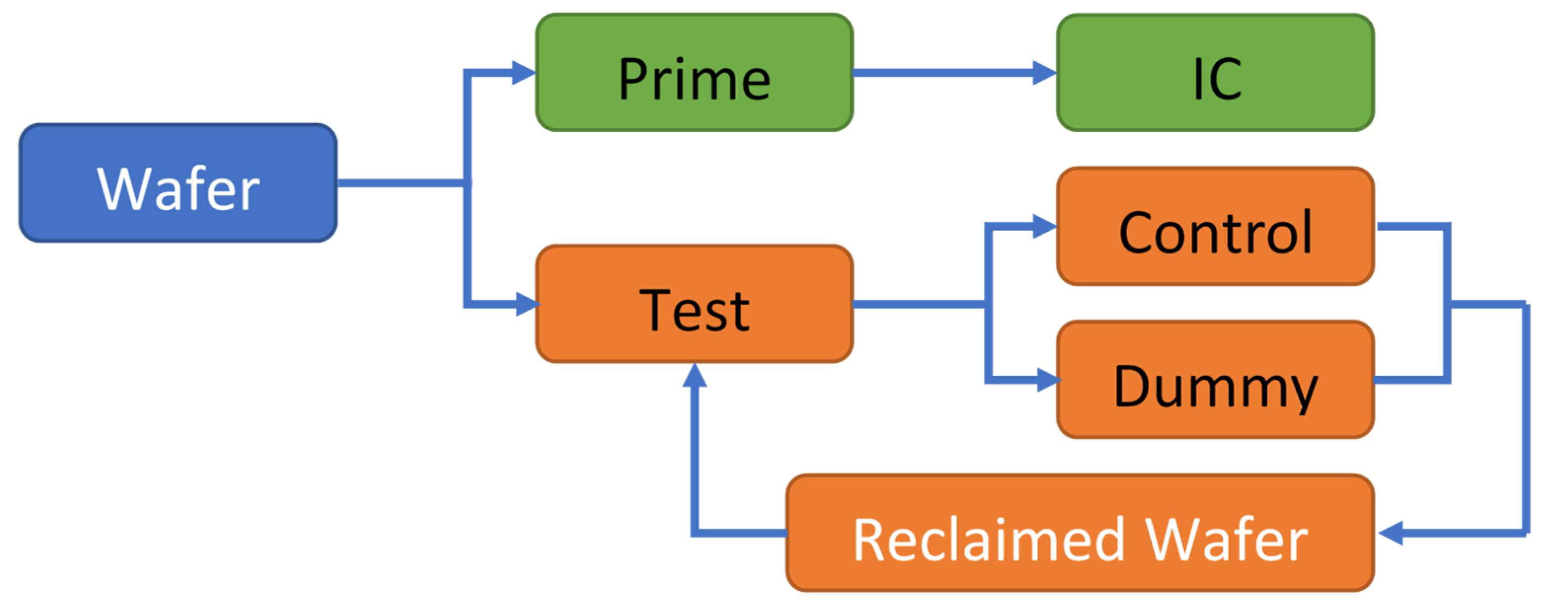
Figure 1. Categories of wafers.
Symmetry 12 00705 g001
Figure 2. Reclaiming process.
Symmetry 12 00705 g002
Figure 3. Defects of reclaimed wafer: (a) Line watermarks; (b) Scratches; (c) Scattered watermarks; (d) Over-etched spots; (e) Water jet; (f) Clustered watermarks; (g) Half-sided watermarks; (h) Eridite residuals; (i) Banded particles.
Symmetry 12 00705 g003aSymmetry 12 00705 g003b
Figure 4. Crystal growth defect: (a) Example image 1; (b) Example image 2; (c) Example image 3; (d) Example image 4; (e) Example image 5; (f) Example image 6.
Symmetry 12 00705 g004aSymmetry 12 00705 g004b
Figure 5. Process of Research.
Symmetry 12 00705 g005
Figure 6. (a) Image with edge; (b) Image with edge and boundary.
Symmetry 12 00705 g006
Figure 7. (a) Before preprocessing; (b) After preprocessing.
Symmetry 12 00705 g007
Figure 8. Rectified linear unit (ReLU) activation function.
Symmetry 12 00705 g008
Figure 9. The basic Structure of convolutional neural network (CNN).
Symmetry 12 00705 g009
Figure 10. (a) Identity shortcut connections; (b)The structure of ResNet 34.
Symmetry 12 00705 g010
Figure 11. Structure of large-scale multilayer perceptron (MLP).
Symmetry 12 00705 g011
Figure 12. (a) Loss of MLP structure 49152-256-10; (b) Loss of MLP structure 49152-256-256-10; (c) Loss of MLP structure 49152-256-256-256-10; (d) Accuracy of MLP structure 49152-256-10; (e) Accuracy of MLP structure 49152-256-256-10; (f) Accuracy of MLP structure 49152-256-256-256-10.
Symmetry 12 00705 g012
Figure 13. Structure of CNN for reclaimed wafers.
Symmetry 12 00705 g013
Figure 14. (a) Loss of CNN structure C8(K3)_F32_F10; (b) Accuracy of CNN structure C8(K3)_F32_F10; (c) Loss of CNN structure C8(K3)_F16_F32_F10; (d) Accuracy of CNN structure C8(K3)_F16_F32_F10; (e) Loss of CNN structure C8(K5)_F16_F32_F10; (f) Accuracy of CNN structure C8(K5)_F16_F32_F10.
Symmetry 12 00705 g014
Figure 15. (a) Loss and accuracy of ResNet 18; (b) A Loss and accuracy of ResNet 34; (c) Loss and accuracy of ResNet 50; (d) Loss and accuracy of ResNet 101; (e) Loss and accuracy of ResNet 152.
Symmetry 12 00705 g015
Table 1. Description of ten typical defects.
TypeDescriptionG/NGNumber of Images
T1Surface with line watermarksG (Re-polishable)78
T2Surface with scratchesG (Re-polishable)638
T3Surface with scattered watermarks G (Re-polishable)39
T4Surface with over-etched spotsG (Re-polishable)40
T5Surface with water jetG (Re-polishable)33
T6Surface with clustered watermarksG (Re-polishable)121
T7Surface with half-sided watermarksG (Re-polishable)77
T8Surface with Eridite residualsG (Re-polishable)139
T9Surface with banded particlesG (Re-polishable)235
T10Crystal growth defectNG1061
Table 2. Setup of training parameters.
Data Split Ratio (Training/Validating)80/20
Learning rate/momentum/decay0.0010/0.9000/1.0000 × 10−6
Loss threshold0.0100
Accuracy threshold0.9975
Patience30 (no improvement in 30 consecutive epochs)
Table 3. Determination of number of hidden layers for MLP.
StructureTraining Loss/AccuracyVal Loss/Accuracy
49152-256-100.1123/0.96800.2992/0.9285
49152-256-256-100.0250/0.99640.1600/0.9687
49152-256-256-256-100.0113/0.99830.0905/0.9777
Table 4. Experiment results of different sizes of the number of hidden neurons.
MLP StructureTraining Loss/AccuracyValidation Loss/Accuracy
49152-256-256-256-100.0113/0.99830.0905/0.9777
49152-256-256-512-100.0082/0.99820.0988/0.9771
49152-256-512-256-100.0255/0.99750.0865/0.9810
49152-512-256-256-100.0079/0.99820.0604/0.9830
49152-256-512-512-100.0129/0.99810.0837/0.9806
49152-512-256-512-100.0173/0.99820.0635/0.9849
49152-512-512-256-100.0097/0.99820.0818/0.9806
49152-512-512-512-100.0089/0.99820.0641/0.9833
Table 5. Determination of the number of convolutional layers for CNN.
NoCNN StructureTraining Loss/AccuracyValidation Loss/Accuracy
1C8(K3_ReLU_MP3)_F32(ReLU)_F10(SM)9.8379/0.12269.7326/0.1270
2C8(K3_ReLU_MP3)_C16(K3_ReLU_MP3)_F32(ReLU)_F10(SM)0.0148/0.99800.0533/0.9878
3C8(K5_ReLU_MP3)_C16(K3_ReLU_MP3)_F32(ReLU)_F10(SM)0.0096/0.99820.0332/0.9936
Table 6. CNN experimental result.
NoCNN StructureTraining Loss/AccuracyValidation Loss/Accuracy
1C8(K3_ReLU_MP3)_C16(K3_ReLU_MP3)_F32(ReLU)_F10(SM)0.0148/0.99800.0533/0.9878
2C8(K3_ReLU_MP3)_C16(K3_ReLU_MP3)_F64(ReLU)_F10(SM)0.0229/0.99820.0656/0.9893
3C16(K3_ReLU_MP3)_C32(K3_ReLU_MP3)_F32(ReLU)_F10(SM)0.0227/0.99600.0677/0.9824
4C16(K3_ReLU_MP3)_C32(K3_ReLU_MP3)_F64(ReLU)_F10(SM)0.0596/0.98070.1548/0.9632
5C8(K5_ReLU_MP3)_C16(K3_ReLU_MP3)_F32(ReLU)_F10(SM)0.0096/0.99820.0332/0.9936
6C8(K5_ReLU_MP3)_C16(K3_ReLU_MP3)_F64(ReLU)_F10(SM)0.0100/0.99810.0278/0.9932
7C16(K5_ReLU_MP3)_C32(K3_ReLU_MP3)_F32(ReLU)_F10(SM)0.0175/0.99810.0224/0.9976
8C16(K5_ReLU_MP3)_C32(K3_ReLU_MP3)_F64(ReLU)_F10(SM)0.0084/0.99810.0313/0.9929
Table 7. ResNet experimental result.
NoResNet StructureTraining Loss/AccuracyValidation Loss/Accuracy
1ResNet 180.8864/0.99800.8930/0.9958
2ResNet 341.6018/0.99761.6090/0.9956
3ResNet 504.8866/0.99814.9844/0.9958
4ResNet 1019.7607/0.99839.7590/0.9962
5ResNet 15213.7344/0.998213.7266/0.9968
Table 8. Comparison between the MLP and CNN.
PerformanceMLP 1CNN_1 2CNN_2 3ResNet 18
Loss (Training/Validation)0.0173/0.06350.0229/0.06560.0175/0.02240.8864/0.8930
Accuracy (Training/Validation)0.9982/0.98490.9982/0.98930.9981/0.99760.9980/0.9958
Train Time (secs per Epoch)47.2 secs43.0 secs30.2 secs51.1 secs
Total number of weights and biases25,439,498235,978119,51411,200,458
1: 16384-512-256-512-10; 2: C8(K3_ReLU_MP3)_C16(K3_ReLU_MP3)_F64(ReLU)_F10(SM); 3: C16(K5_ReLU_MP3)_C32(K3_ReLU_MP3)_F32(ReLU)_F10(SM).
Table 9. Confusion Matrix of CNN_2 Network.
ActualPrediction
Type 1Type 2Type 3Type 4Type 5Type 6Type 7Type 8Type 9Type 10
Type 12636000000000
Type 203005051000000
Type 30025540000000
Type 40002587000000
Type 50000250100000
Type 60000026020000
Type 70000002565000
Type 80000000267600
Type 90000000028210
Type 100000000002573