1. Introduction
In recent years, the aerospace industry has developed rapidly, and more and more electronic systems are working in the radiation environment. Radiation effects, especially single-event effects (SEEs), are the main cause of electronic systems failure in the radiation environment [
1,
2]. When the energetic particles hit the sensitive region of the electronic device, their energy is deposited in the body region of the device. Additionally, the particle ionizes a large amount of charge on its incident trajectory. The charge is collected by the device electrodes. Then, a significant current is created and the drain voltage is changed. This effect is single-event transient (SET).
There has always been a strong interest from the radiation effects community in fully-depleted silicon-on-insulator (FDSOI) technologies, given their resistance against single-event effects (SEEs) due to the presence of a buried oxide (BOX) layer [
3,
4]. At the same time, FDSOI devices are good candidates as technology scales down beyond 28-nm node, with a superior control of the short channel effects (SCEs) and low power consumption [
5,
6].
In space, aerospace chips often work at extremely low temperature or high temperature, so the study of the correlation between temperature and single-event transient (SET) effects has never stopped [
7,
8]. The previous studies proposed that the SET pulse width increases with temperature for the bulk process, but not for the FDSOI process [
9,
10]. As the process scales down, the electrical characteristics of the transistor at the process node below 45 nm exhibit an anti-temperature effect. The transistor delay increases with the temperature decreasing [
11]. Whether the temperature dependence of SET pulse width in 28-nm FDSOI technology is still consistent with the conclusion in large scale process is worthy to study.
Furthermore, as the process scales down, the supply voltage continues to drop. Especially, 28-nm FDSOI devices can work at ultra-low supply voltage of 0.4 V to achieve ultra-low power consumption [
12]. However, it is well known that the drop in the supply voltage brings great challenges to the performance of the circuit, and increases the sensitivity of the single-event effect significantly [
13,
14]. Therefore, the ultra-low supply voltage dependence of SET in 28-nm FDSOI technology needs to be studied. The temperature dependence of SET at low supply voltage is also worthy to investigate.
2. Device Structure and Simulation Setup
Due to the good look-inside capability, three-dimensional(3D) TCAD simulation has been proven to be a useful means for investigating digital SET and the mechanism of the single event charge collection [
15,
16,
17,
18]. The 3D-TCAD models are established to simulate the SET in FDSOI devices. Sentaurus TCAD vN-2017.09-SP1 from Synopsys was used in our work. All simulations were conducted using the YINHE computing cluster in National University of Defense Technology in China.
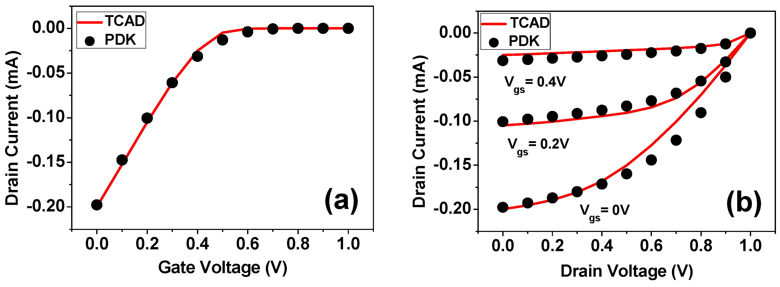
28-nm FDSOI NMOS and PMOS device are built and calibrated with the 28 FDSOI PDK. For the 3D-TCAD device model and spice model in the PDK, we obtained good agreement with the I-V characteristics in the 258 K to 398 K range. The high-K dielectric layer and metal gate technology is used.
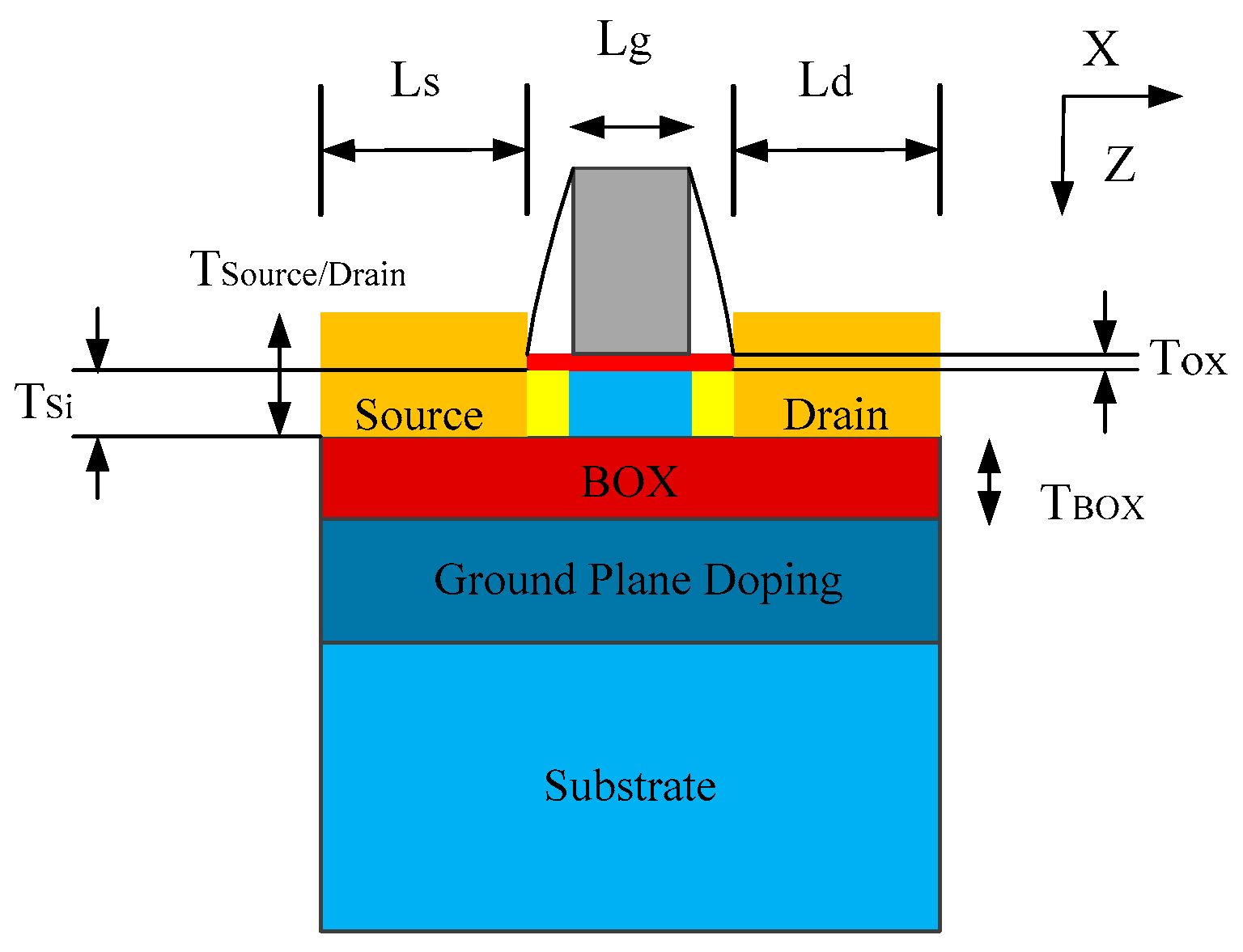
Figure 1 shows a cross-sectional schematic diagram of the 28-nm FDSOI device. Design parameters are listed in
Table 1.
Figure 2 shows the I-V characteristic curves of the NMOS device.
Figure 3 shows the I-V characteristic curves of the PMOS device.
The NMOS and PMOS device are connected to an inverter during TCAD simulations. The total simulation time is Ts = 3000 ps and the heavy ion impacts at Ti = 100 ps. All simulations are conducted for normal incidence. Only the off-state device is sensitive to SET. The heavy ions strike the off-state devices at the center of the gate, and the linear energy transfer (LET) is 40MeV-cm2/mg. The supply voltage of the devices is various from 0.4 V to 1.2 V, and the temperature is various from 258 K to 398 K. The collected charge is given by the drain current integration over the transient duration.
The following physical models were used: (1) Fermi-Dirac statistics, (2) band-gap narrowing effect, (3) doping dependent SRH recombination and Auger recombination, (4) temperature, doping, electric field and carrier-carrier-scattering impact on mobility, and (5) incident heavy ions were modeled using a Gaussian radial profile with a characteristic 1/e radius of 50 nm and a Gaussian temporal profile with a characteristic decay time of 0.25 ps. Hydrodynamic model was used for carrier transport. Unless otherwise specified, default models and parameters provided by Sentaurus TCAD vN-2017.09-SP1 (Synopsys, Mountain View, CA, USA) were used.
3. Simulation Results
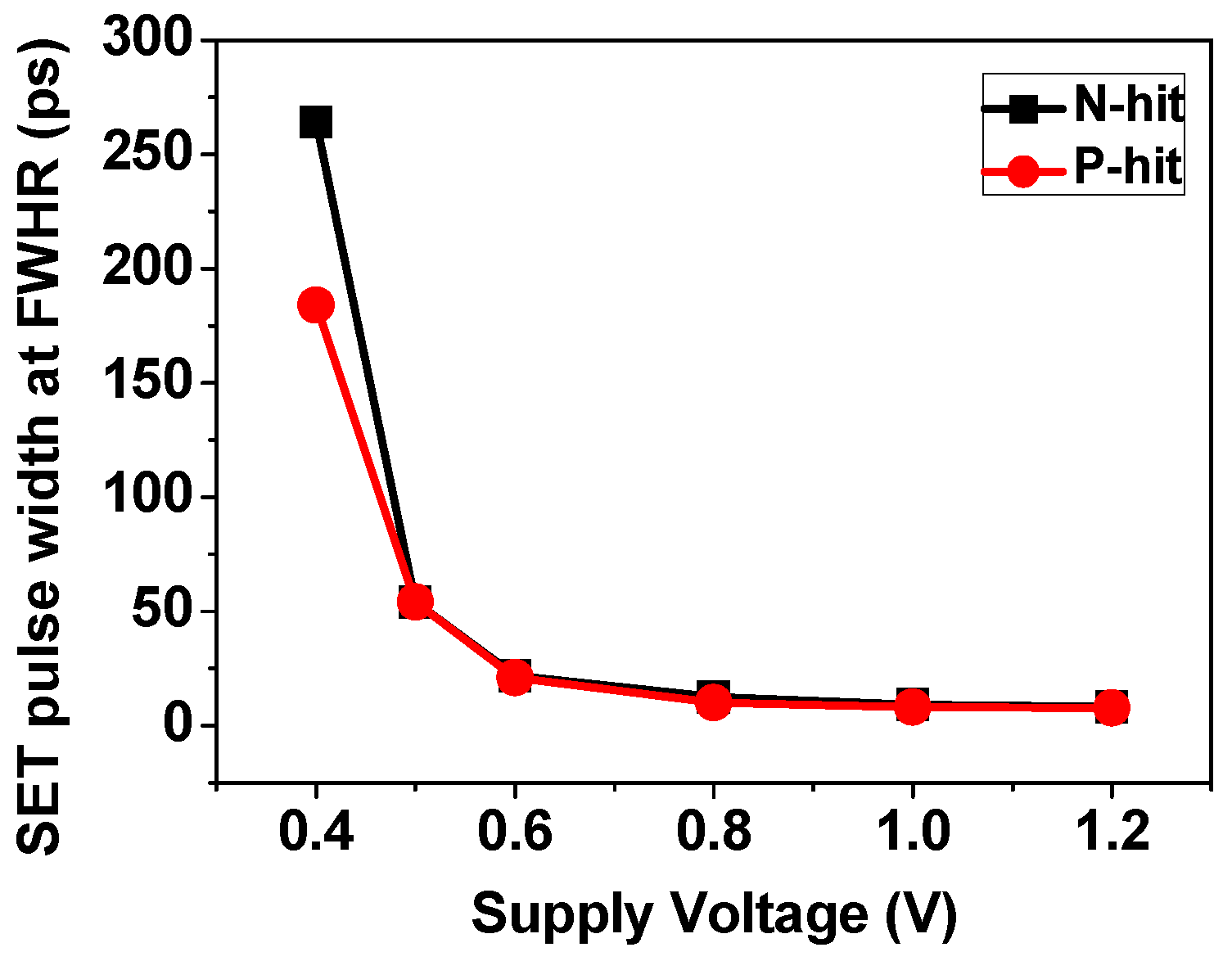
The supply voltage dependence of the SET pulse width in 28-nm FDSOI device was investigated by varying the supply voltage from 0.4 V to 1.2 V. Additionally, the temperature is 300 K. For brevity, in this paper, that heavy ions strike the NMOS devices and PMOS devices are denoted as N-hit and P-hit, respectively. The inverter input is low at N-hit and the inverter input is high at P-hit. The simulation results are shown in
Figure 4. The SET pulse width increases as the supply voltage decreases. When the supply voltage is below 0.6 V, the SET pulse width increases sharply with the decrease of the supply voltage. N-hit produces a wider SET than P-hit at 0.4 V.
Under different supply voltages, the effect of temperature on the SET pulse width is quite different. This work takes N-hit as an example because NMOS devices are more sensitive to SET than PMOS devices in FDSOI process [
19] and the conclusions of N-hit and P-hit are similar.
Figure 5 shows the SET pulse generated by N-hit at temperatures of 258 K, 300 K, and 398 K when the supply voltage is from 0.4 V to 1 V. When the supply voltage is 0.8 V and 1 V, the temperature dependence of SET is very low, and the SET pulse width is slightly wider at a high temperature than at a low temperature. However, when the supply voltage is below 0.6 V, the situation is completely different. The SET pulse width exhibits an anti-temperature effect, that is, the SET pulse width is wider at a low temperature than at a high temperature. Besides, the anti-temperature effect is significantly enhanced as the supply voltage drops. When the supply voltage is 0.4 V, the SET pulse width at 398 K is 8.5 times that at 258 K.
4. Discussion
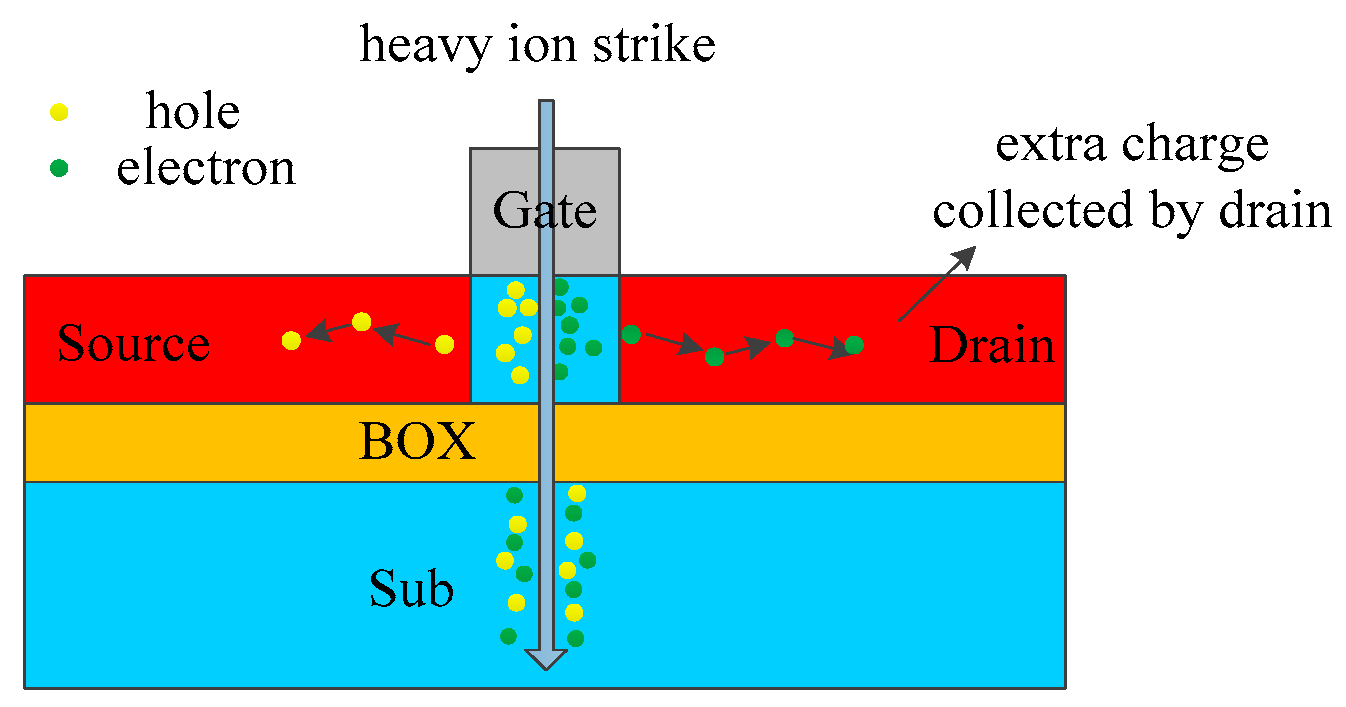
When the heavy ions hit the sensitive region of the electronic device, their energy is deposited in the body region of the device. Additionally, the heavy ion ionizes a large amount of charge on its incident trajectory. The charge is collected by the device electrodes. Then, a significant current is created and the drain voltage is changed. As shown in
Figure 6, this phenomenon is SET.
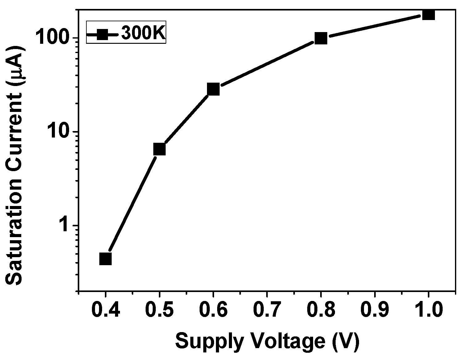
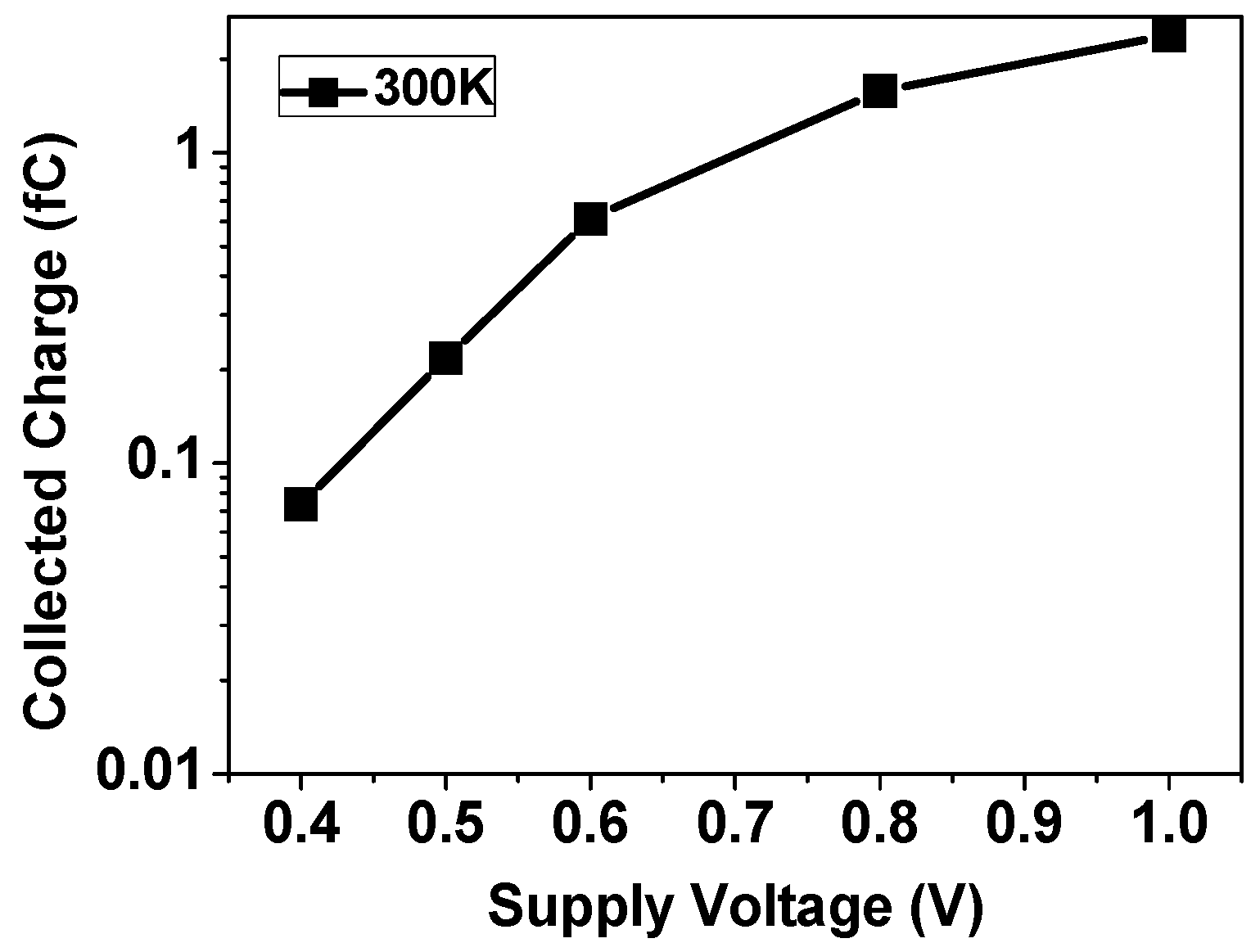
The SET pulse width is directly related to the charge collection and the saturation current of the transistor. The SET pulse narrows as the saturation current increases, and becomes wider as the charge collection increases. Therefore, the effects of supply voltage and temperature on saturation current and charge collection should be compared separately.
As shown in
Figure 7, the saturation current decreases as the supply voltage decreases, and the saturation current decreases faster when the supply voltage becomes smaller. The saturation current at 0.5 V is 14.7 times that at 0.4 V, and the saturation current at 1 V is just 1.8 times that at 0.8 V. As shown in
Figure 8, the charge collection also decreases as the supply voltage decreases. The charge collection at 0.5 V is 2.9 times that at 0.4 V, and the charge collection at 1 V is 1.5 times that at 0.8 V. The effect of supply voltage on the saturation current is clearly dominant. Therefore, the SET pulse width increases as the supply voltage decreases. When the supply voltage is below 0.6 V, the SET pulse width increases sharply with the decrease of the supply voltage.
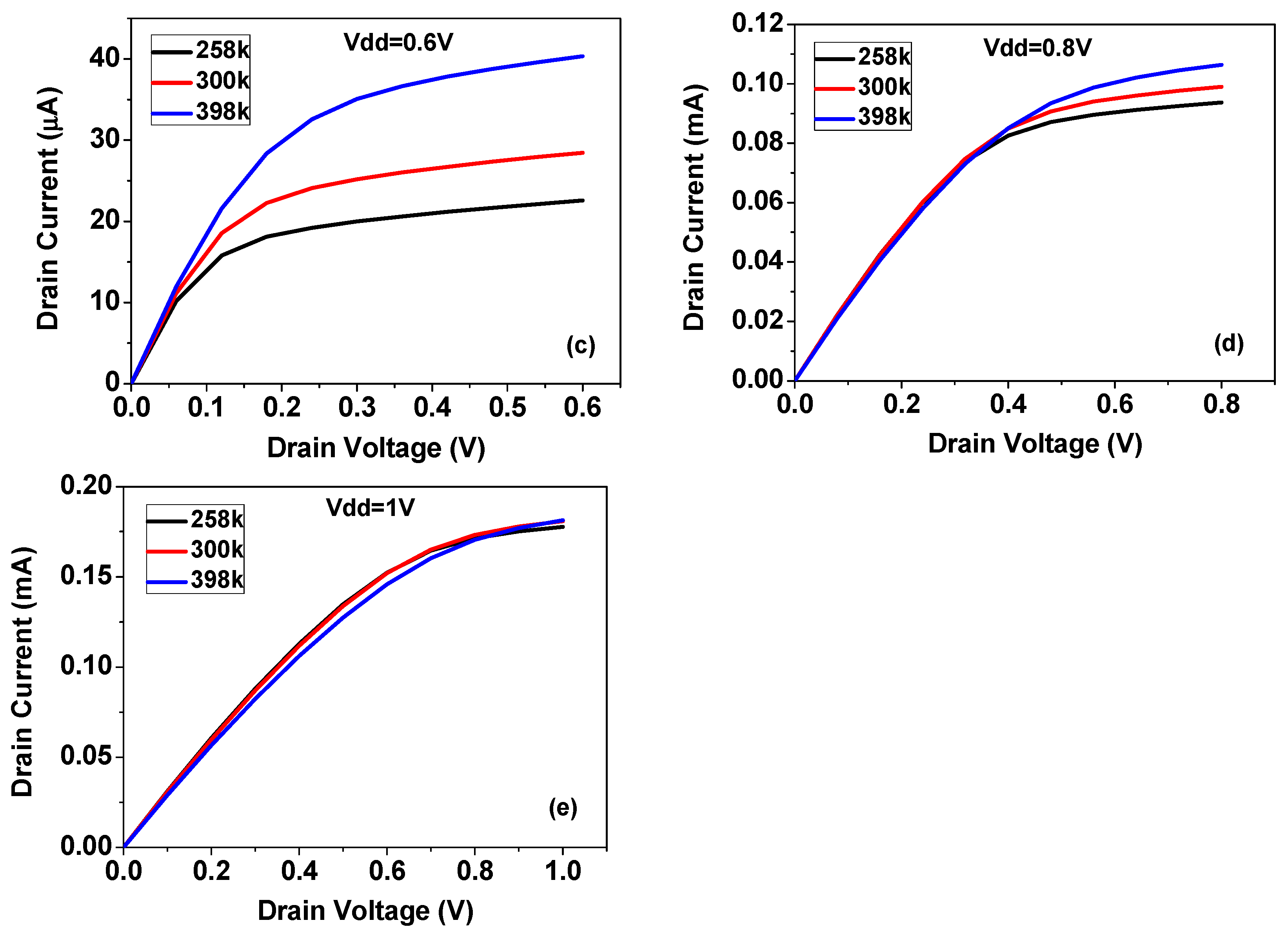
Figure 9 shows the I-V curve of the NMOS device at temperatures of 258 K, 300 K, and 398 K when the supply voltage is from 0.4 V to 1 V. Obviously, the temperature has a slight influence on the I-V curve of the transistor when the supply voltage is 1 V. However, as the supply voltage decreases, the influence of the temperature on the saturation current is larger and larger. Additionally, as the temperature decreases, the saturation current decreases. When the supply voltage is 0.4 V, the saturation current at 398 K is 33 times that at 258 K.
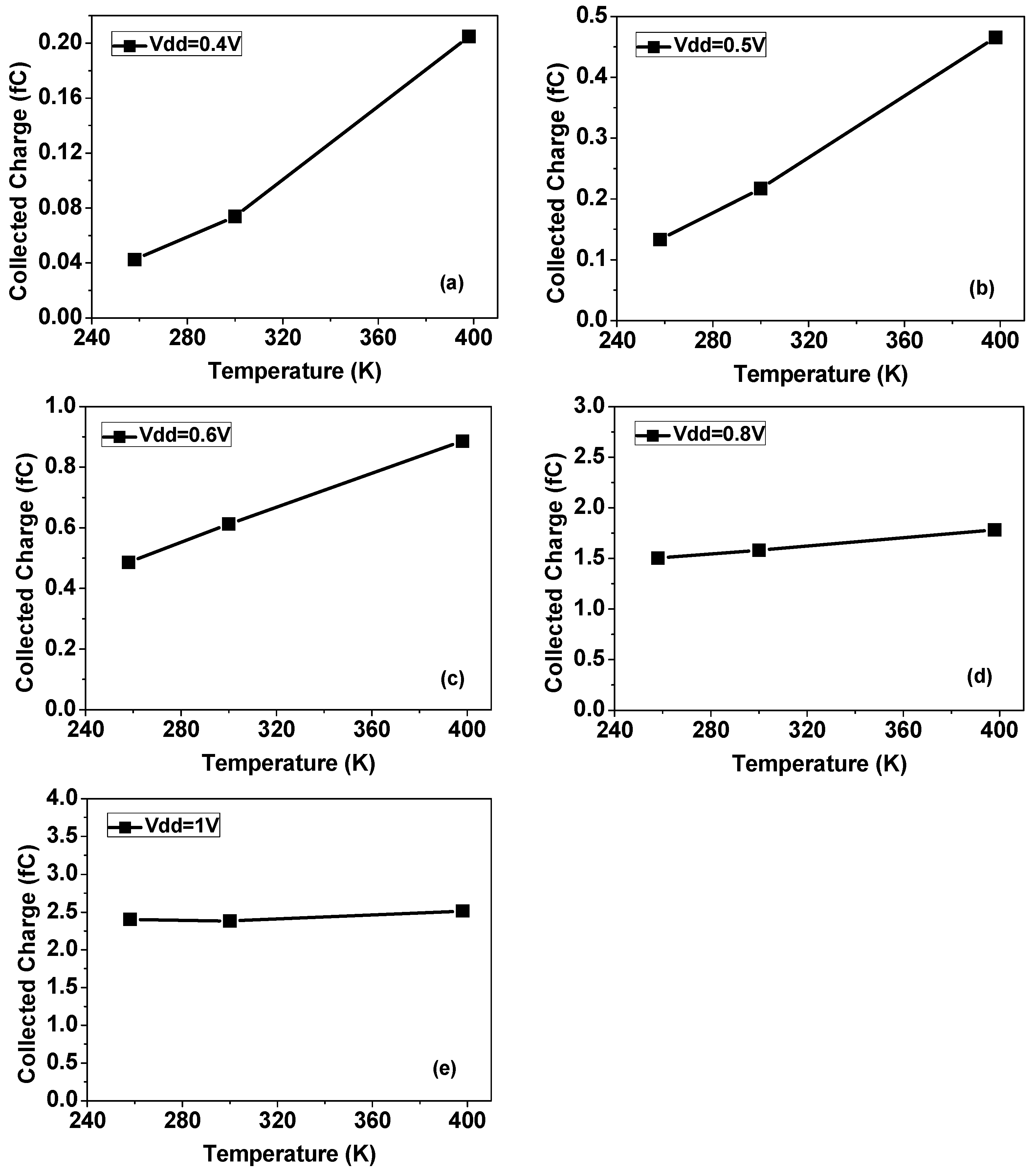
Figure 10 shows the charge collection of the NMOS device at temperatures of 258 K, 300 K, and 398 K when the supply voltage is from 0.4 V to 1 V. As shown in
Figure 10, the temperature has a slight influence on the charge collection of the transistor when the supply voltage is 1 V. However, as the supply voltage decreases, the influence of the temperature on the charge collection is larger and larger. Additionally, as the temperature increases, the amount of charge collection increases. When the supply voltage is 0.4 V, the charge collection at 398 K is 5 times that at 258 K.
Due to the mechanism of SET, there are two reasons for determining the SET pulse width. One is the charge collection and the other is the recovery current. The recovery current depends on the transistor saturation current. The SET pulse narrows as the saturation current increases, and becomes wider as the charge collection increases. As Vdd (the supply voltage) decreases, the influence of the temperature on the saturation current and the influence of the charge collection both are larger and larger. Additionally, as the temperature increases, the saturation current and the charge collection both increase.
However, the effects of the saturation current and the charge collection on the SET pulse width are reversed. Therefore, it depends on whether the two are offset each other or one of them plays a leading role. At Vdd = 1 V, the temperature has no effect on both, so it has no effect on the SET pulse width. At Vdd = 0.8 V, the temperature has a similar effect on both, so they offset each other and have little effect on the SET pulse width. At Vdd = 0.6 V, the effect of temperature on the saturation current is greater than the effect on the charge collection, so the SET pulse narrows as the temperature increases. At Vdd = 0.5 V and 0.4 V, the effect of temperature on the saturation current is completely dominant, so the SET pulse width shows a significant temperature dependence. When the supply voltage is 0.6 V or less the SET pulse width exhibits an anti-temperature effect, and the anti-temperature effect is significantly enhanced as the supply voltage drops.
5. Conclusions
The SET pulse width increases as the supply voltage decreases. When the supply voltage is below 0.6 V, the SET pulse width increases sharply with the decrease of the supply voltage. The SET pulse width is not sensitive to temperature when the supply voltage is 1 V, because the temperature has a slight influence on the saturation current and the charge collection. However, when the supply voltage is 0.6 V or less, the SET pulse width exhibits an anti-temperature effect, and the anti-temperature effect is significantly enhanced as the supply voltage drops. The effect of temperature on the saturation current is clearly dominant. This work is the first to reveal the supply voltage and temperature dependence of SET pulse width in 28-nm FDSOI technology completely.
Author Contributions
Funding acquisition, B.L.; Methodology, R.S.; Project administration, Y.G.; Software, Y.C.; Writing—original draft, J.X.; Writing—review & editing, J.X.
Funding
This work is supported by the Natural Science Foundation of China (Grant No. 61804180 and Grant No. 61434007).
Acknowledgments
Thanks for Errui Zhou’s help in this work.
Conflicts of Interest
The authors declare no conflict of interest.
References
- Dodd, P.E.; Shaneyfelt, M.R.; Schwank, J.R.; Felix, J.A. Current and future challenges in radiation effects on CMOS electronics. IEEE Trans. Nucl. Sci. 2010, 57, 1747–1763. [Google Scholar] [CrossRef]
- Schrimpf, R.D.; Warren, K.M.; Weller, R.A.; Reed, R.A.; Massengill, L.W.; Alles, M.L.; Fleetwood, D.M.; Zhou, X.J.; Tsetseris, L.; Pantelides, S.T. Reliability and radiation effects in IC technologies. In Proceedings of the 2008 IEEE International Reliability Physics Symposium, Phoenix, AZ, USA, 27 April–1 May 2008; pp. 97–106. [Google Scholar] [CrossRef]
- Simoen, E.; Gaillardin, M.; Paillet, P.; Reed, R.A.; Schrimpf, R.D.; Alles, M.L.; Mamouni, F.E.; Fleetwood, D.M.; Griffoni, A.; Claeys, C. Radiation effects in advanced multiple gate and silicon-on-insulator transistors. IEEE Trans. Nucl. Sci. 2013, 60, 1970–1991. [Google Scholar] [CrossRef]
- Gaillardin, M.; Paillet, P.; Ferlet-Cavrois, V.; Baggio, J.; McMorrow, D.; Faynot, O.; Jahan, C.; Tosti, L.; Cristoloveanu, S. Transient Radiation Response of Single- and Multiple-Gate FD SOI Transistors. IEEE Trans. Nucl. Sci. 2007, 54, 2355–2362. [Google Scholar] [CrossRef]
- Luan, S.; Liu, H.; Jia, R.; Cai, N. The dynamic reliability of ultra-thin gate oxide and its breakdown characteristics. Acta Phys. Sin. 2008, 57, 2524–2528. [Google Scholar]
- Chouksey, S.; Fossum, J.G.; Agrawal, S. Insights on Design and Scalability of Thin-BOX FD/SOI CMOS. IEEE Trans. Electron. Devices 2010, 57, 2073–2079. [Google Scholar] [CrossRef]
- Liu, Z.; Chen, S.; Chen, J.; Qin, J.; Liu, R. Parasitic bipolar amplification in single event transient and its temperature dependence. Chin. Phys. B 2012, 68, 607–612. [Google Scholar] [CrossRef]
- Chen, S.; Chen, J. Temperature dependence of the P-hit single event transient pulse width in a three-transistor inverter chain. Chin. Phys. B 2012, 21, 340–345. [Google Scholar] [CrossRef]
- Chen, S.; Liang, B.; Liu, B.; Liu, Z. Temperature Dependence of Digital SET Pulse Width in Bulk and SOI Technologies. IEEE Trans. Nucl. Sci. 2008, 55, 2914–2920. [Google Scholar] [CrossRef]
- Gadlage, M.J.; Ahlbin, J.R.; Ramachandran, V.; Gouker, P.; Dinkins, C.A.; Bhuva, B.L.; Narasimham, B.; Schrimpf, R.D.; McCurdy, M.W.; Alles, M.L.; et al. Temperature dependence of digital single-event transients in bulk and fully-depleted SOI technologies. IEEE Trans. Nucl. Sci. 2009, 56, 3115–3121. [Google Scholar] [CrossRef]
- Kumar, R.; Kursun, V. Reversed Temperature-Dependent Propagation Delay Characteristics in Nanometer CMOS Circuits. IEEE Trans. Circuits Syst. II Express Briefs 2006, 53, 1078–1082. [Google Scholar] [CrossRef]
- Shang, H.S.H.; White, M.H.; Adams, D.A. 0.25V FDSOI CMOS technology for ultra-low voltage applications. In Proceedings of the 2002 IEEE International SOI Conference, Williamsburg, VA, USA, 7–10 October 2002; pp. 37–38. [Google Scholar] [CrossRef]
- Kauppila, J.S.; Kay, W.H.; Haeffner, T.D.; Rauch, D.L.; Assis, T.R.; Mahatme, N.N.; Gaspard, N.J.; Bhuva, B.L.; Alles, M.L.; Holman, W.T.; et al. Single-Event Upset Characterization Across Temperature and Supply Voltage for a 20-nm Bulk Planar CMOS Technology. IEEE Trans. Nucl. Sci. 2015, 62, 2613–2619. [Google Scholar] [CrossRef]
- Mitrović, M.; Hofbauer, M.; Voss, K.-O.; Zimmerman, H. Experimental Investigation of the Joint Influence of Reduced Supply Voltage and Charge Sharing on Single-Event Transient Waveforms in 65-nm Triple-Well CMOS. IEEE Trans. Nucl. Sci. 2018, 65, 1908–1913. [Google Scholar] [CrossRef]
- Ferlet-Cavrois, V.; Paillet, P.; Gaillardin, M.; Lambert, D.; Baggio, J.; Schwank, J.R.; Vizkelethy, G.; Shaneyfelt, M.R.; Hirose, K.; Blackmore, E.W.; et al. Statistical analysis of the charge collected in SOI and bulk devices under heavy ion and proton irradiation—Implications for digital SETs. IEEE Trans. Nucl. Sci. 2006, 53, 3242–3252. [Google Scholar] [CrossRef]
- Mavis, D.G.; Eaton, P.H. SEU and SET modeling and mitigation in deep submicron technologies. In Proceedings of the 2007 IEEE International Reliability Physics Symposium Proceedings, Phoenix, AZ, USA, 15–19 April 2007; pp. 293–305. [Google Scholar] [CrossRef]
- Chen, J.; Chen, S.; Liang, B.; Liu, B.; Liu, F. Radiation hardened by design techniques to reduce single event transient pulse width based on the physical mechanism. Microelectron. Reliab. 2012, 52, 1227–1232. [Google Scholar] [CrossRef]
- Zhang, J.; Chen, J.; Huang, P.; Li, S.; Fang, L. The Effect of Deep N+ Well on Single-Event Transient in 65 nm Triple-Well NMOSFET. Symmetry 2019, 11, 154. [Google Scholar] [CrossRef]
- Gadlage, M.J.; Gouker, P.; Bhuva, B.L.; Narasimham, B.; Schrimpf, R.D. Heavy-Ion-Induced Digital Single Event Transients in a 180 nm Fully Depleted SOI Process. IEEE Trans. Nucl. Sci. 2009, 56, 3483–3488. [Google Scholar] [CrossRef]
© 2019 by the authors. Licensee MDPI, Basel, Switzerland. This article is an open access article distributed under the terms and conditions of the Creative Commons Attribution (CC BY) license (http://creativecommons.org/licenses/by/4.0/).
