Abstract
The investigation of size effects appearing in the dependence of AlGaN/GaN HEMT high-frequency characteristics on channel width d and number of sections n is conducted using the notions of measure, metric and normed functional (linear) spaces. In accordance with the results obtained, in local approximation the phenomenon of similarity can exist, not only in metric spaces of heteroepitaxial structures, but also in the defined on them functional spaces of the measures of these structures’ additive electrophysical characteristics. This provides means to associate size effects of the HEMTs with their structure material fractal geometry. The approach proposed in the work gives an opportunity, not only to predict the size of the structural elements (e.g., channel width and number of sections) of the transistor with the desired characteristics, but also to reconstruct its compact model parameters, which significantly speeds up the development and optimization of the HEMTs with the desired device characteristics. At transferring to the global approximation, when the topological and fractal dimensions of the structure coincide, its electrophysical characteristics, and subsequently, the values of the compact model equivalent circuit parameters, as well as HEMT high frequency characteristics, follow the classic (linear) laws peculiar to the spaces of integer topological dimensions DT.
1. Introduction
Investigations of the influence of the electric charge carrier chaotic motion on non-linear effects in the transfer characteristics of semiconductor devices (e.g., field-effect transistors, FETs) have been conducted since the 1960s. It has been revealed that in general cases, non-periodic and non-regular chaotic signal fluctuations follow the theory of deterministic chaos, and in local approximation can be described in notions of geometry of fractal dimensions [1,2,3,4]. In the result, it has become clear that at submicron- and nanoscale, the conventional wisdom about current flow being a drift-diffusional process can no longer be used for a precise description of FET electrical characteristics. One example for it is the model of charge carrier kinetics in the layer of the fractal structure, using the mathematical tool of the fractal integro-differentiation [5].
In the capacity of the contribution to the problem under consideration, this work studies the basic concepts of the Hausdorff–Bezikovich fractal dimension geometry, investigates the peculiarity of AlGaN/GaN heteroepitaxial structure (HES) geometry, determines the main geometric factors affecting high frequency (HF) HEMT characteristics, conducts experimental tests involving an analysis of HES electrophysical parameters pk,i, measurement of manufactured transistors’ HF characteristics H21(f), Gmax(f), fT, and fmax, extraction of the parameters Pk,i of their linear models and a verification and physical interpretation of the results obtained. The listed actions are taken in the context of the application in semiconductor materials science and exemplified by heterostructural AlGaN/GaN field-effect transistors with high electron mobility (hereinafter referred to as HEMTs).
2. The Basic Concepts of Fractal Geometry in the Context of Its Application for the Description of AlGaN/GaN HEMT Structures
Until recent times, the limitedness of the application of chaos theory and fractal geometry in semiconductor materials science was associated with the beliefs about the linearity of the processes taking place on the surface and in the volume of heteroepitaxial structures, and nonlinearities observed in general were explained by defects, dopants and crystalline anisotropy. In actual fact, nonlinear properties can be intrinsic to crystalline semiconductors. For example, distribution of dopants, defects, relief irregularities [6,7] and surface potential lateral irregularities, as well as processes of deposition, crystal nucleus formation and growth, and also mosaic structure of epitaxial films, have nonlinear chaotic character [4,8,9,10,11,12]. Due to their small sizes, such objects, as well as the quantum ones, can be considered as nanoscale objects in semiconductor electronics.
In local approximation (when the measurement scale linear size l is lower than some value L), physical parameters pk,i of the nano- and microstates of the objects listed above often have the properties of chaotic systems [8,9,10,11,12] including: (1) a strong dependence of the system state on initial condition (small changes of environmental condition lead to significant changes of the state); (2) relativity and indefiniteness of the measurement processes, i.e., dependence upon the choice of reference coordinates and the measurement scale; (3) existence of topological mixing properties—when components do not overlap each other [7]. As reported in [4], all of these properties can be used to improve the characteristics of the developed semiconductor devices.
The properties mentioned above often lead to the occurrence of so-called size effects, i.e., the dependence of the measures of semiconductor electronics objects under testing on the linear sizes of their structural elements [6,7]. In view of this, today the theory of deterministic chaos based on nonlinear (e.g., fractal [6,7]) geometry is used more and more widely to calculate (simulate) the classic and quantum transfer characteristics of semiconductor devices at submicron- and nanoscale levels.
Despite a growing number of investigations into this sphere [13,14,15,16], the nature of size effects in semiconductor device engineering, and specifically, its inquiry for the purpose of improving FET device characteristics, remain understudied. This is one of the main reasons why today there is no possibility to reliably predict the HF small signal and power characteristics of field-effect transistors in relation to the linear size of their structural elements (e.g., width of sections d and their number n — number of fingers). In other words, the development and optimization of transistor parameters have, in general, an experimental search nature today.
2.1. Using Linear Functional Spaces for a Description of Semiconductor Object Electrophysical Characteristics
The investigation of the influence of the AlGaN/GaN heteroepitaxial structure geometry upon the device characteristics of HEMTs based on that structure was conducted using the notions of measure, metric and normed linear functional spaces (hereinafter referred to as functional spaces), which gave an opportunity to consider scalar and vector values, continuous functions and number sequences from the same point of view.
One of the important characteristics determining the application scope for the Euclidian geometry of integer topological dimensions DT is the limit of local approximation L—the value of linear scale. When the measurement scale l of any linear size of a semiconductor object goes beyond the local approximation limit L (i.e., where l > L), the Hausdorff–Bezikovich dimension DH of this object becomes equal to its topological dimension: DH = DT. This is an applicable scope of Euclidian geometry. When the linear size l of the object is less than or equal to L (l ≤ L), the Hausdorff–Bezikovich dimension DH of the object becomes less than its topological dimension DT: DH < DT. In this scope the DH value can be fractional.
In most cases, only functions being essentially integrals of some non-negative additive functions determined at the families of Minkovsky space sets, which satisfy triangle, symmetry and zero distance axioms [17], are considered for definition of measures M. The Minkovsky space is a four-dimensional pseudo-Euclidian space of the signature {1,3} [18].
At this, for every function it is necessary to consider only families of Minkovsky space sets measurable by the given measure M for which this measure exists. In the capacity of such spaces let us use metric spaces R formed by the pair R = {X, ρ}, consisting of some set of semiconductor device elements of construction and heteroepitaxial structure X = {xi}, in which the distance ρ between any pair of elements is defined with the triangle, symmetry and zero distance axioms [17,19]. In this case, a single-valued, non-negative real function ρ = ρ(r) must be defined for any r (r is a radius-vector) from the X set.
The set of surface points (relief) can be counted as the metric space of the heteroepitaxial structure; the FET structural element set X (the set of ohmic and barrier contacts, field-effect gates, etc.) in which the distance between any pair of elements is defined with the triangle, symmetry and zero distance axioms, can be counted as the FET metric space R = {X, ρ}. For example, in FET metric spaces we can consider subsets R* in which ρ is defined by the number of sections n and/or channel width d: ρ = n × d = W. It is obvious that these subsets have all the properties of the basic set. So hereinafter we are going to use R instead of R*. This approach gives an opportunity to investigate the geometry of semiconductor electronics objects, but it does not help to reveal the relation of this geometry and the electrophysical properties of the objects.
In the context of semiconductor materials science and device engineering, depending on the task in any individual case, it is necessary to use functional spaces which properties are defined by the class of the used functions (the type of metric) describing one of the object electrophysical parameters pk,i. Unlike metric spaces R, the measures of functional spaces (functionals Φ) can also have negative values, e.g., the measures of electrical charge, resistance, current density, etc. Specifically, integrals of electrical charge, current or mass density functions can be considered as the measures revealing the capacitive, conductive and mass-dimensional properties of line wire, two-dimensional surfaces or three-dimensional objects [20,21,22,23].
Let us consider the integral of some function Fk (x,y,z)—functional Φk—as the measure in the functional space Mk = Φk:
The relation between functional and metric spaces can be built by an association of each area from the metric space set R with some functional Φk,i from the linear functional space Mk = {Φk,i}—the set of functions describing measures Φk,I = Mk,i of the kth additive (integral) physical characteristic of the semiconductor object, where k = 1, 2, … K is a number of such measure, characterizing for example, M1,I = Rgs,i, M2 = Rds,i, M3 = Cgs,i, M4 = Cgd,i, M5 = Cds,i, M6 = gmax,i, and many others, and I = 1, 2, … , … N is a number of the element with the kth measure. At this, all arguments of the functions Fk,i from the linear functional spaces Mk must belong to the metric space set R.
Therefore, each area from the metric space set R can be matched with an integral measure Mk,i (functional) from the functional space, describing through the arguments belonging to the metric space R some additive (integral) electrophysical characteristic.
The association of R and Mk forms the so-called “metric space with a measure” SM,k = {R, Mk}, that is essentially an assembly of the elements of this metric space R, on which some measure set Mk,i from the linear functional space Mk [12,17] depends (through the arguments). In this case the dimension of both metric spaces R and functional spaces Mk can be represented by any one of the real numbers from 0 to 3.
In the context of transistors, the set X of transistor structure points belongs to the metric spaces R = {X, ρ}, and the set of measures of their electrophysical and device characteristics {Mk,i} belongs to functional spaces. Thus, we obtain the metric space with a measure SM,k = {R, Mk} that is essentially an assembly of elements of the transistor metric space R, to which parts some set Mk of measures Mk,i of the transistor electrophysical and device characteristics is assigned [12].
2.2. Measures of Semiconductor Objects’ Physical Parameters
In semiconductor materials science, in the local limit (l < L) the measure M of such (e.g., fractal) objects can generally be represented by any additive value: mass; defect, charged particles or irregularities density; surface, interface or heterojunction area; diffusion front shape, etc.
The problem of the definition of semiconductor object measure M involves the definition of how many times N the object under measurement, which is enclosed with a limited space RD, can be filled with some measuring (gauge) object described by the function , where γ is a normalizing index, δ is a dimensionless scale, DM is a Minkovsky dimension (the dimension of the limited set in metric space). Then, according to [7], . As in the given paper we are going to work only with a subset of metric spaces and functional subspaces defined on them, let us use the Hausdorff–Bezikovich dimension DH (hereinafter referred to as the Hausdorff dimension) instead of the Minkovsky dimension DM, because these notions are close enough DH ≈ DM [7]. Therefore, the dimension DH of a limited set in metric space can be represented in the following way:
where η is a minimum number N of diameter d sets, with which it is possible to lay down (fill) a set under measurement, if the value d is decreased by a factor of ζ [7].
Then, the semiconductor object measure M can be written in the following way:
The Hausdorff–Bezikovich dimension DH relates to the fractal dimension Df as Df = DT + DH, where DT = 1, 2, 3 is an integer topological dimension.
In the case of self-similar (e.g., fractal) sets, the Hausdorff dimension can be considered as a similarity dimension DS = DH.
If the known value of the measure M0 of some semiconductor object under investigation is taken as a normalizing index γ(D) in Equation (4), the expression can be written in the following way:
After taking the logarithm of both left and right parts we obtain an expression for the dimension Df represented through the object measure M:
It is worth reminding ourselves that an ideal fractal object is formed by the embedded non-overlapping sets of self-similar forms, and can be characterized by the following parameters: local approximation limit L, fractal dimension Df, scaling indexes ζ and η, the law of affine transformation xi = Axi−1 [7]. Recall that at l ≥ L, Df = DT.
At the same time, naturally the most Brownian and chaotic objects, which semiconductors can be counted as, are not self-similar in the literal sense. It is possible to consider only some statistical similarity and statistical self-affinity—the similarity in some interval of measurement scales characterizing with an average per set fractal dimension value. However, the object under investigation can be characterized, not by one, but by several fractal dimension values depending upon the measurement scale l, Df = Df(l)—the so-called multifractal object. In such cases it is often convenient to use an average value of fractal dimension <Df> which is obtained by means of averaging out fractal dimensions determined for different surface sections [24].
With some simple transformations it is possible to reveal that in the local approximation (l < L) the relation of the measures of fractal objects corresponding to different linear dimensions d has more gently-sloping power-law dependence than in global approximation (l ≥ L):
From Equation (7) it is possible to define the value Df:
The object measure Mi+1 of the following similarity level:
It follows from Equation (9) that at transferring to global approximation (at l ≥ L), where DT = Df, the relation of measures M follows the standard law:
For example, in a local approximation a three-times change in the linear size of the side of the projection on the (x,y) plane of the square section d × d of the fractal surface with Df = 2.36, leads to the change of its measure Md (e.g., surface electric charge), not in times, but much less, to be exact, just in 34−Df = 34−2.36 = 31.64 ≈ 6.06 times (7). Simultaneously, a relative value of some variable Md(d), say electrical charge density σd = Md(d), is fully defined by the linear size d of the section under measurement:
where d0 is a linear size of the projection onto the (x,y) plane.
Upon transferring to global approximation, when Df = DT, the expression (1) is transformed into the conventional, invariant with d, expression:
Therefore, the mathematical relations (9) and (11) describe a law which allows, in local approximation, the control the physical properties of semiconductor objects at the nanoscale level by means of changing their linear sizes d, in a far greater (>>100 nm) interval of measurement scales compared to the one for quantum objects (≤100 nm).
As functional space subsets exhibit the metric space basic properties of triangle, symmetry and zero distance, the expressions (6) and (8) can be used to define their Hausdorff dimensions. In this case, M0 must be represented by the highest or the lowest value of the functional at the functional space under investigation, corresponding to the smallest l = l0 or to the largest l = lmax value of our measurement scale. Assuming η = Φk,i/Φk,0 and ζ = li/l0, from Equation (3) it is possible to define the values DS of functional spaces, e.g., layer resistances [12].
To estimate the operating peculiarities of the AlGaN/GaN transistors under investigation, we will use a small-signal model (SS-model), which elements belong to linear functional spaces SM,k = {R, Mk}, defined depending on n and d in some area of metric space R = {X, ρ(n, d)} of these transistors’ structural elements. The SS-model in a form of equivalent circuit (EC) is essentially an assembly of k = 1…K interacting equivalent elements Pk,i [25,26] belonging to some SM,k. The used field-effect transistor EC rather accurately describes the behavior of HEMT small-signal S-parameters in a frequency range up to 60 GHz [27].
3. The Connection between the Electrophysical Parameters of the AlGaN/GaN HEMT Heteroepitaxial Structure and Its Geometry
In this section, we investigate in local approximation the connection between the geometry and electrophysical characteristics of the used AlGaN/GaN heteroepitaxial structure (HES) grown on a semi-insulated sapphire wafer with the diameter of ≈50 mm by means of the metalorganic chemical vapor deposition (MOCVD) technique. The thickness of the semi-insulating buffer gallium nitride (GaN) layer is 2000 nm, the one of the aluminum nitride (AlN) layer is 1.5 nm, the Al30Ga70N spacer is 4 nm; the thicknesses of the high-alloy (ND > 1018 cm−3) AlxGa1−xN:Si n+ layer and encapsulating unalloyed GaN layer are 14 nm and 2 nm, correspondingly. Electron density of two-dimension (2D) electron gas NS = 1.36 × 1013 cm−2, mobility μ (at T = 300 K) = 1200 cm2/(V × s), and the dislocation density is ~108 cm−2 [22,28].
For the purpose of HES conductivity estimation, the matrix of test elements with different width d and channel length lds has been formed on one part of the structure. The elements have the form of active rectangular areas with thickness d insulated from each other by means of reactive ion etching.
On the areas there are parallel-plate ohmic contacts (OC) with the distance lds between any two of them (Figure 1a), formed by means of explosive lithography, TiAlNiAu deposition and subsequent annealing in nitrogen atmosphere at the temperature of 780 °C during 30 s.
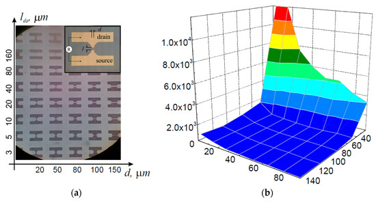
Figure 1.
The optical image of the matrix of TiAlNiAu ohmic contacts of the test elements with different values of channel length lds and width d, formed on the AlGaN/GaN high-electron-mobility transistor (HEMT) heteroepitaxial structure—(a). The dependence of the channel resistance per unit length ρ on the length lds and width d—(b).
In order to define the HES Hausdorff dimension, we used tracing—a technique based upon the similarity dimension DS definition by calculating the number of closed contours [7] encircling surface irregularities in the (x,y) plane, or lateral irregularities of electrostatic potential. After the tracing we calculated the number N0 of closed contours obtained at the given measurement scale l0. At the next stage, scale li was decreased to obtain an integer number of closed contours Ni > N0, and so on, until li was equal to the minimum distance between pixels. With the use of expression (3), taking into account that η = Ni−1/Ni and ζ = li−1/li, we defined the metric space similarity dimension DS for the surface under investigation. A graphical representation of the closed contour number Ni vs. li is called “freaking stairs”, due to different height and width of its steps (Figure 2a,b).
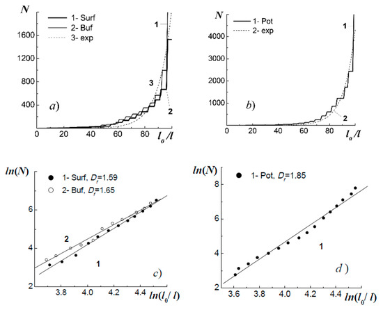
Figure 2.
The “freaking stairs” for the 50 × 50 µm areas of the relief surfaces of the AlGaN/GaN HEMT heteroepitaxial structure (polyline 1), gallium nitride (GaN) buffer layer (polyline 2), and their exponential approximation (curve 3)—(a); the “freaking stairs” for the contact potential difference (CPD) Δφ(x;y) of the AlGaN/GaN heteroepitaxial structure (polyline 1) and its exponential approximation (curve 2)—(b). The linear dependences of ln(N) on ln(l0/l) for the surface areas of AlGaN/GaN HES structure (line 1) and GaN buffer layer (line 2)—(c); the same dependence for the contact potential difference (CPD) Δφ(x;y) of AlGaN/GaN heteroepitaxial structure—(d).
Measurement of electrophysical parameters pk,i and estimation of HEMT HES surface relief shape h(x,y) (Figure 3a) were conducted with the use of the Solver-HV atomic force microscope (AFM)—made by NT-MDT (Zelenograd, Moscow)—in semi-contact mode [29]. The contact-potential difference (CPD) Δφ(x,y) between cantilever needle point and HEMT HES (Figure 3b) was measured by means of the AFM Kelvin probe technique in semi-contact mode with the use of the following expression:
where φp was a surface potential of the cantilever needle point plating material (p for probe), and φS was a potential of the surface (s for surface) under investigation. Therefore, being aware of the work function of the cantilever needle point (qφp), from the expression (13) it was possible to find out the distribution of potential φS(x,y) (or work function qφS) throughout the surface area under investigation. AFM measurements were conducted in air in semi-contact mode with the use of the a double-pass technique with the resolution of 65,536 pixels (NN = 256 points in vertical and horizontal sweeps). The maximum size of the AFM scan area was equal to 100 × 100 µm2. In order to provide semi-contact mode, NSG10 cantilevers were used, which needles had tungsten carbide W2C plating with electron work function of ≈4.9 eV. The instrument influence of the other structural elements of the cantilever at the contact point was not more than 25%.
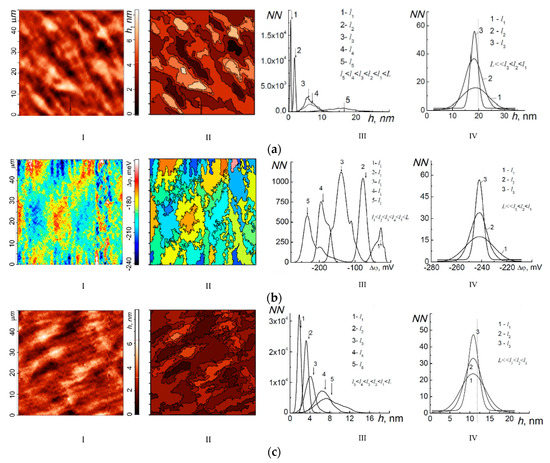
Figure 3.
The atomic force microscopy (AFM) images of 50 × 50 µm surface areas (column I): (a) the relief h(x;y) of the AlGaN/GaN HEMT structure; (b) irregularities of surface potential Δφ(x;y); (c) the relief h(x;y) of the GaN buffer layer—with the corresponding contour images (column II) and distribution histograms in local (column III) and global (column IV) approximations.
Figure 3a(I) shows the results of the Brownian relief h(x,y) initial check for the HES surface area of 50 × 50 μm. The investigation was conducted with the use of the AFM techniques described above. Statistical studies demonstrate that the average values of the relief irregularities <h> depend on the measurement technique. As distribution bar charts h(NN) show, at NN = Const, the decrease of the measurement scale li = ai/NN < L through the reduction of the studied area side length a leads to a monotonous decrease of the surface irregularities and roughness average values <h> and <Ra>, correspondingly, in a row: for the area of 100 × 100 µm (l = 390 nm) <h> = 15.41 nm and <Ra> = 3.24 nm, for the area of 50 × 50 µm (l = 195 nm) <h> = 8.47 nm and <Ra> = 1.99 nm, for the area of 30 × 30 µm (l = 117 nm) <h> = 6.59 nm and <Ra> = 1.32 nm, for the area of 10 × 10 µm (l = 39 nm) <h> = 1.84 nm and <Ra> = 0.21 nm and for the area of 5 × 5 µm (l = 19.5 nm) <h> = 0.65 nm and <Ra> = 0.11 nm (Figure 3a(III)).
Conversely, in the case of l decreasing through the increase of scan points number NN at the constant size of the area under investigation (a = Const = 50 µm), the average values <h> and <Ra> grow: at N = 1256 (l = 50/1024 = 0.049 µm = 49 nm) <h> = 15.91 nm and <Ra> = 3.51 nm, at N = 512 (l = 98 nm) <h> = 9.13 nm and <Ra> = 1.59 nm, at N = 256 (l = 195 nm) <h> = 6.89 nm and <Ra> = 1.44 nm, at N = 128 (l = 391 nm) <h> = 2.73 nm and <Ra> = 0.51 nm, and at N = 64 (l = 781 nm) <h> = 2.68 nm and <Ra> = 0.31 nm. These data reveal indefiniteness and relativity of the AlGaN/GaN HES surface relief estimation results (e.g., <h> and <Ra>) in the local limit at l < L, and this is one of the basic attributes of chaotic systems [6,7].
Another necessary attribute which gives an opportunity to consider the area surface of the structure under investigation as a chaotic system in local approximation is its strong dependence on environment conditions: Small changes in conditions of growth and processing lead to significant changes in the state of the surface, specifically in relief shape and surface potential.
The investigation of surface geometry by means of tracing shows that at every r = li/li+1 -fold decrease of the measurement scale l we obtain a discrete sequence of the embedded sets of non-overlapping contours (Figure 3a(II)) with a step-like increase of their number N(l)—“freaking stairs” (Figure 2a). Figure 3a(II) shows that shapes of the embedded lateral contours of relief irregularities are not self-similar in a literal sense. It is only possible to speak about some statistical self-similarity. The existence of the self-similarity properties of the HES surface area under investigation is revealed by the linear dependence of ln(N(l)) on ln(l0/l) (Figure 2c), which makes it possible to consider the observed objects as fractal, or (at the presence of several kinks in linear dependence of ln(N(l)) on ln(l0/l)) multifractal ones. These results are indicative of the topological mixing properties of the HES under investigation that is a third attribute of chaotic systems.
The average relief values <h> measured in the global approximation at L < l3 = 50 µm, l2 = 100 µm, l1 = 150 µm (l3 < l2 < l1) reveal classic dependence: as the measurement scale l decreases, dispersion decreases too (Figure 3a(IV)). In global approximation, l is defined by a step of an AFM objective table along the axes x and y.
An initial check of surface potential irregularities Δφ(x,y) (11) with the use of AFM techniques (Figure 3b(I)) shows the maximum spread of the values up to 90 mV.
Filling contours obtained after tracing the lateral irregularities of the surface potential form non-overlapping embedded sets (Figure 3b(II)), and these linear sizes in the (x,y) plane, just like the lateral sizes of the relief irregularities, depend upon the measurement scale l. In this case, the existence of the attributes of statistic self-similarity, and subsequently fractality, is proven by the linear dependence of ln(N(l)) upon ln(l0/l) (Figure 2d). As Figure 2b shows, the “freaking stairs” can be well approximated with the exponent.
The statistical analysis of the CPD = Δφ(x,y) irregularities distribution (Figure 3b(III)) also reveals the relativity and indefiniteness of the measurement process. It was shown that a decrease of the size a of the investigated surface area side at NN = Const leads to a decrease of the average values <Δφ(x,y)>, and vice versa, the increase of NN at a = Const leads to an increase of <Δφ(x,y)>. This, in its term, reveals in the local approximation (l < L) the relativity and indefiniteness of the measurement process for the AlGaN/GaN HEMT heteroepitaxial structure surface electrostatic potential.
The environmental conditions exert a strong influence over the average value and the shape of lateral irregularities Δφ(x,y). Even a slight change in growth and processing conditions leads to significant changes in Δφ(x,y).
As the result it becomes obvious that in local approximation, the distributions of lateral irregularities of the HES surface potential also have all of the attributes of chaotic systems, which makes fractal geometry a mathematical instrument suitable for their description.
The average values <Δφ> measured in global approximation also exhibit known classic dependence common to integer topological dimensions: as the measurement scale l decreases, the dispersion decreases too (Figure 3b(IV)).
The value of the local approximation limit L for relief irregularities and lateral surface potential irregularities is not less than 100 µm—due to AFM device limitations.
The direct investigation of the HES conductive capacity depending on the test element channel width d and length lds was conducted on the probing station M-150 (Cascade Microtech, Beaverton, Oregon, USA) with the use of the B-1500 semiconductor device parameter analyzer (Keysight Technologies, Santa Rosa, California, USA). To exclude serial resistance of the probe-to-surface contact, the four probes Kelvin technique was used. The resistance measurement error in the bias range from −5 to +5 V was not more than 0.04 Ω.
Static current–voltage curves of test elements show that, while d > 30 µm and lds > 60 µm, sheet resistance (resistance per square) ρ▯ = (d × Rds)/lds ≈ Const (Figure 1b) within the scope of the admissible values, and channel resistance Rds and drain saturation current Ids have virtually linear dependence on d and lds. If d and lds are equal to or less than given values (d ≤ 30 µm, lds ≤ 60 µm), the value ρ▯ = ρ▯(d, lds) becomes a function of d and lds (Figure 1b), and there is nonlinear dependence of values Rds = Rds(d, lds) and Ids = Ids(d, lds). As the result, it is possible to conclude that the given HES sheet resistance ρ▯ = ρ▯(d, lds) depends largely on channel length lds and width d in the range of practically valuable measurement scales (linear sizes)—that is size effect.
Therefore, it was shown that for AlGaN/GaN HEMT HES in local approximation, size effects were exerted in fractal dependence of its electrophysical parameters values on linear sizes n and d.
Based on the results obtained, it is possible to give the following physical explanation for size effects observed in a given case. The maximum size of irregularities (the level difference of 20–30 nm) and surface relief shape of the grown heteroepitaxial layers (Figure 3a(I)) virtually replicate the relief shape and irregularity size of buffer layer (Figure 3c(I)). It means that heteroepitaxial layers forming a HEMT structure replicate the buffer layer surface irregularities. The analysis of the contour relief image (Figure 3c(II)) shows that its scaling indices ζ and η, and ones of the HES, have close values. At the same time statistical analysis of relief irregularities reveals the same results both in local (Figure 3c(III)) and global (Figure 3c(IV)) approximations.
The facts stated above give the basis to assume that electrons of 2D electron gas move from the source to the drain, not in the two-dimensional, but in the three-dimensional plane, by-passing irregularities of the 2D channel or scattering on them. It is obvious that the number of scattering events is in a direct ratio with the number of scattering centers that are 3D irregularities of 2D channel spread throughout the (x,y) plane in a fractal way. In this case elastic scattering is the reason for the change of the electron pulse vector, and in the general case, it leads to the decrease of the absolute value of their group speed vector component. In the case of non-elastic scattering the quantity of energy lost by electrons is also in direct ratio with the number of scattering centers that are spread throughout the area of the heterojunction in a fractal way, as said above. In both cases, it leads to an increase of channel resistivity Rds, and consequently to the growth of specific values Rsg and Rdg.
In addition to 2D channel irregularities, the point scattering centers can influence on the electron motion in two-dimensional electron gas. These centers are positive ions of shallow-level impurity ND+, which concentration in the material is equal to 2 × 1018 cm−3. In order to study the geometry of the irregularity distribution ND+(x,y) by the Kelvin method with the use of AFM, the geometry of the CPD irregularity distribution Δφ(x,y) was investigated. It is possible to estimate that at an average level of the doping of the AlGaN epitaxial layer ND+ = 2 × 1018 cm−3, the Debye shielding distance (space charge region, SCR) is equal to 17–20 nm that is comparable with the HES thickness. This means that SCR irregularities born by the unequal (fractal) distribution of the ionized shallow-level donor impurity ND+ come to the surface, forming there surface potential lateral irregularities distributed in a fractal way. It follows that positive ions of shallow-level donor impurity are also distributed in this fractal way throughout the area of the two-dimensional electron gas. At this, as it is shown in Figure 3b, the lateral sizes of such irregularities can exceed 50 µm (limited by the sizes of the area under investigation). The investigations of the 100 × 100 µm surface areas reveal that in this case L can be significantly more than 100 µm. The more precise definition of L is restricted by the technical capabilities of the used AFM. It is clear that the fractal distribution of the ionized shallow-level donor impurity forming heteroepitaxial level capacity and consisting of the scattering centers has great influence virtually on all parameters Pk,i of the internal transistors of the EC linear model.
In summary, it is possible to assume that the observed size effects can significantly influence on both statistic [28,30,31] and high-frequency (HF) [32,33,34] device characteristics of the HEMTs under investigation.
4. AlGaN/GaN HEMT Manufacturing
The paper investigates a 4 × 5 transistor matrix (Figure 4a) manufactured on the basis of HESs described above (see Section 3). Mesa insulation of the active area with the thickness of 50 nm was formed by means of photoresist mask reactive ion etching. The ohmic contacts (OK) of the drain and the source (D–S) were built using the processes of explosive lithography, TiAlNiAu plating and consecutive annealing in a nitrogen atmosphere at the temperature of 780 °C during 30 ns. The channel length lds (the distance between the drain and the source) was equal to 5 µm. After that the whole structure was covered with SiO2 dielectric film of the first mask having the thickness of 0.15 µm, and then with the resist. The openings were formed in the resist mask by means of lithography methods. The edges situated closer to the drain corresponded to the position of the Schottky gates of the fabricated transistors. Then, according to the resist mask, openings in the first dielectric mask were formed by means of chemical etching. The etching time was estimated by vision—until the total elimination of dielectric layer from the surface of the structure. After the resist elimination, the second lithography was conducted to create openings, surrounding the edges of the dielectric mask corresponding to the gate positions. The resist mask edge was situated closer to the drain located on the dielectric surface, and the second one was located on the surface of the channel active area. As a result, there was a gap with the length of ~0.15 µm on the HES surface between the dielectric and the resist masks. Therefore, the opening length in the resist mask defined the size of the gate cap, and the offset of the mask relative to the dielectric edge defined the gate length lg. After NiAu deposition and explosion we obtained the L-shaped “Field-plate” gate with the length lg = 0.15 µm, which cap was shifted to the drain (Figure 4b). At final stage, the glassivation of the structure active area was performed using an SiO2 dielectric. Then, the openings in this dielectric over the pads were created in order to connect the sources of all transistor sections by air bridges and to perform the galvanic thickening of the drain, source and gate pads.
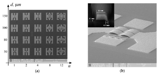
Figure 4.
The electron microscopy images: the 5 × 4 matrix of AlGaN/GaN HEMTs with section number n = 1, 2, 4, 8 and 12 and section width d = 50, 80, 100 and 150 µm—(a); the AlGaN/GaN HEMT crystal 4 × 100 µm with the L-shape gate length of 0.15 µm (insertion)—(b).
As the result, at the same chip a matrix of AlGaN/GaN HEMTs with lg = 150 nm was formed. HEMTs differ from each other, not only by section number n = 1, 2, 4, 8 and 12, but also by channel width dds = 50, 80, 100 and 150 µm (Figure 4a).
5. The Methods of Measurement and Extraction of AlGaN/GaN HEMT Linear Models
In order to validate the stated assumption about the HES fractal geometry impact on AlGaN/GaN HEMT high-frequency parameters, the reconstruction of the values (measures Mk,i) of the equivalent circuit components Pk,i of the SS model for all transistors in the matrix was performed.
For the purpose above, the measurement of small-signal S-parameters of the manufactured HEMTs in the frequency range of 0.1–40 GHz was performed in accordance with the techniques described in [35,36,37,38,39]. The supply voltage was Uds = 20 ± 1 V. The insignificant spread of Uds is due to the optimization of current operating points to achieve maximum values of H21 and Gmax. The measurement was carried out with the use of the PNA-X N5245A 2-port vector network analyzer (Keysight Technologies, Santa Rosa, California, USA) at the Summit 12,000 semi-automatic probe station (Cascade Microtech, Beaverton, Oregon, USA). The calibration of measuring paths of the ports 1 and 2 of the vector network analyzer was performed by the Line-Reflect-Reflect-Match (LRRM) method [35] with measuring S-parameters of the gage structures: (1) microstrip line, per passing through (Thru); (2) 50 Ω load (Load); (3) open-circuit test element (Open); and (4) short-circuit test element (Short).
After that, the de-embedding procedure for the measured S-parameters was performed according to the technique described in [36,37,38,39]. This procedure involved elimination of the influence of the parasitic parameters of the pads, measuring probes and other elements of the measuring assembly, on the measurement results. For the de-embedding we used test elements which had the form of short-connected (“short”) and opened (“open”) pads of gates, drains and sources. Frequency dependences of power Gmax(f) (Figure 5a) and current H21(f) (Figure 5b) amplification factors of the manufactured HEMTs point out that in average they are compliant with the world analogs.
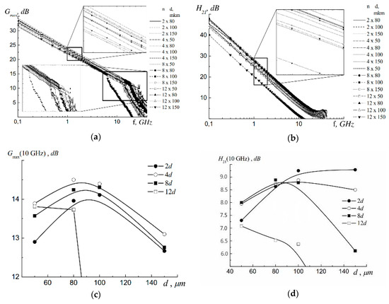
Figure 5.
The frequency dependences of maximum values of the power and current amplification factors Gmax(f)—(a) and H21(f)—(b), correspondingly. The functional dependences Gmax = Gmax(d)—(c) and H21 = H21(d)—(d), measured at different values of n at frequency f = 10 GHz.
In this paper, the reconstruction (extraction) of the parameters Pk,i of the SS model EC components by the measured S-parameters was carried out in accordance with the combined technique [40,41] incorporating advantages of analytic [26] and optimization [39] methods of the extraction.
According to [9,26,32], the procedure of HEMT small-signal EC extraction included three main stages.
At the first one, the external parasitic parameters of the transistor were defined from the transistor measurements obtained in “cold” modes (at drain zero voltage) and at direct current using techniques represented in [36,37,38].
At the second stage, the Y-parameters of the internal transistor were defined by means of the subtraction of the external components according to the technique described in [36]. The accuracy of the determination of the internal frequency-independent components is strongly dependent upon the accuracy of the external parameters definition. The solution of the equation system binding the Y-parameters obtained and the parameters of internal components makes it possible to reconstruct the parameter values for these components [37].
At the third stage, the optimization of the values of the internal transistor equivalent circuit components was performed in order to get the best correspondence between the measured and simulated S-parameters. Based on the frequency independence of the internal components [38], an additional objective function was formed—the minimum mean-square deviation of the parameters of the internal components from their constant values [39]. The optimizable values were the parameters of the external components Lg, Ls, Ld, Rg, Rs and Rd of the transistor equivalent circuit (Figure 6).
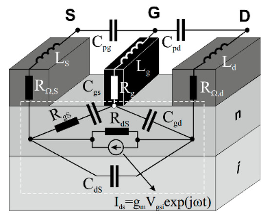
Figure 6.
The equivalent circuit of the linear model of field-effect transistor. The components of the internal transistor are circled with a dotted line.
As it is seen in Figure 6, there are internal (encircled with the dotted line: Rgs is gate-source resistance; Rds is drain-source resistance of the depletion region; Cgs is gate-source capacity; Cgd is gate-drain capacity; Cds is drain-source capacity; Ids is drain current source controlled by the gate-source voltage; gmax is transconductance; τ is a time constant of the frequency dependence of the current source) and external parts of the field-effect transistor small signal model EC.
In the general case, the values of the HEMT EC external parameters are defined by the parasitic parameters of the assembly components (e.g., pads, connection leads, plated holes). In this paper they are not considered.
The analysis of size effects i.e., the dependences of the measures Mk of the parameters Pk obtained after extraction of the internal transistor EC components on the number of sections n and their width d, was carried out using the notion of Hausdorff–Bezikovich non-integral dimension DH (fractal Df) [7] (see Section 2).
In order to estimate the field effect transistor operation at high frequencies, we use their peak characteristics: maximum current amplification factor H21 at short-circuit termination, maximum power amplification factor Gmax ≡ MUG (maximum unilateral gain) in the absence of the feed-back inside the transistor, current-amplification cutoff frequency fT, and power-amplification cutoff frequency fmax.
Conventionally the maximum amplification factors H21 and Gmax are defined through the parameters of scattering matrix (S-matrix) using the following known expressions:
where k is the parameter of stability defined as:
where is determinant of the scattering matrix.
The physical sense of the frequency fT is specified by the time of electron transmission through the distance between source and drain lds with the group saturation velocity vsat:
The physical sense of the frequency fmax characterizes the maximum oscillation frequency up to which the transistor acts as the active component. At the extrapolation of this frequency the transistor begins to act as the passive one.
Power- and current-amplification cutoff frequencies fmax and fT are determined from the following clause: amplification factors [Gmax] = dB and [H21] = dB are equal to the one.
The value of fmax can be both higher and lower than fT, which is defined by transistor structure peculiarities in every individual case.
6. Experimental Results (Size Effects in AlGaN/GaN HEMT HF Characteristics)
From (14)–(17) it is seen that H21, Gmax, fT, and fmax do not explicitly depend upon n and d, as these expressions describe the behavioral structureless model of the field-effect transistor.
At the same time, HF characteristics of the HEMTs under investigation reveal that Gmax(f) (Figure 5a) and H21(f) (Figure 5b), as well as fT and fmax (Table 1), have non-monotonous dependence on the number n and the width d of the transistor sections. The comparison of the measured values of current- and power-amplification cutoff frequencies fT and fmax for all n and d shows that they cannot be uniquely described by the known expressions (17) and (18).

Table 1.
The cutoff frequencies fT and fmax of the manufactured AlGaN/GaN HEMTs with the gate length lg = 0.15 μm, at various n and d.
Therefore, the analysis of experimental small-signal parameters Gmax and H21 at the frequency f = 10 GHz was carried out for all test structures. The experimental dependences (Figure 5c) and (Figure 5d) are non-monotonous and have maxima over both n and d. Thus, for Gmax the maximum is observed at d = 80–100 µm and n = 2, and for H21 at n = 4 at the same values of d, which agrees with the results stated in [34].
Therefore, the experimental results clearly demonstrate the size effect revealed in the dependence of HEMT HF characteristics upon both the number of sections n and their width d.
In order to find out the reasons for dependence of H21(f) and Gmax(f), and correspondingly, fT and fmax, on n and d, let us compare the internal transistor linear model parameter values Pk,i reconstructed in accordance with the technique described above. In the general case, the increase of n and d leads to the proportional (linear) increase of the total width of the transistor channel W = n × d. In the context of transistor EC, it is identical to a parallel connection of elementary resistances and capacitances in the internal transistor model. In accordance with Ohm’s law, it should result in a linear change of the resulting EC resistances and capacitances, i.e., the measures Mk of transistor parameter values Pk,i. However, as it is shown below, in real transistors this situation takes places only in particular cases.
Table 2 contains extracted parameter values (measures Mk,i) of internal transistor EC components, grouped by a common feature—the width of the individual section d of the transistor. Thus, data selection 1-1 includes the transistors with d = 50 µm (n = 4, 8 and 12), data selection 1-2—the transistors with d = 80 µm (n = 2, 4, 8 and 12), data selection 1-3—the transistors with d = 100 µm (n = 2, 4, 8 and 12), and data selection 1-4—the transistors with d = 150 µm (n = 2, 4, 8 and 12).
Table 2.
The parameters Pk,i of the AlGaN/GaN HEMT internal transistor EC components, grouped by channel width d = Const.
The grouping by channel width d reveals the dependence of specific parameter values Pk,i* = Pk,i/Wi on section number n: . In each selection the increase of n leads to a slight decrease of specific capacity C/W and transconductance gm/W and to a significant decrease of specific resistance R/W. The dimensions DH(Cds) and DH(Cgd) show the same behavior—their values decrease as n increases. Vice versa, the values DH(Cgs) and DH(Rds) increase as n increases. With the n growth the value DH(Rgs) increases for the selection m1, decreases for the selection m2, increases for the selection m3 and decreases again for the selection m4. The comparability of the dimension values DH(Cgs) with DH(Rds), as well as DH(Cgd) with DH(Rgs) and DH(gmax) means that the physical mechanisms of the operation of internal transistor parameters Cgs and Rds, as well as Cgd, Rgs and gmax are defined by similar geometric dependences.
Table 3 shows the same parameter measure values grouped by another common feature—the number of sections n in the transistor—for the EC components of internal transistors of the same test structure. Data selection 2-1 consists of transistors with n = 2 (d = 80 µm, 100 µm and 150 µm), data selection 2-2 includes transistors with n = 4 (d =5 0 µm, 80 µm, 100 µm and 150 µm), data selection 2-3 incorporates transistors with n = 8 (d = 50 µm, 80 µm, 100 µm and 150 µm) and data selection 2-4 gathers transistors with n = 12 (d = 50 µm, 80 µm, 100 µm and 150 µm).
Table 3.
The parameters Pk,i of the AlGaN/GaN HEMT internal transistor EC components, grouped by section number n = Const.
The grouping by the parameter n in some cases leads to the similar changes of parameter values depending on d (Table 3). Thus, the increase of d per data selection results in the slight decrease of specific values and more significant decrease of the values and . At this, the values for the data selections 2-1 and 2-2 decrease, and for the data selections 2-3 and 2-4, having greater values of d, do not virtually change. With the increase of d the specific values decrease for the data selection 2-1, have minimum value for the data selection 2-2, decrease again for the data selection 2-3 and have maximum value for the data selection 2-4. The behavior of specific values in this case has also some peculiarities. The increase of the parameter d virtually in no way influence on the values g*m,max in data selection 2-1, leads to the growth of g*m,max values in data selections 2-2 and 2-3, results in slight change of g*m,max in data selection 2-4. The dimensions DH(Cgd) and DH(Cds) have almost the equal values slightly changing at the change of d. The values DH(Cgs) change inappreciably for data selections 2-1 and 2-2, and grow with d growth for data selections 2-3 and 2-4. The DH(gm) values decrease as d increase.
There is an illustrative variant of the comparison when transistors have the same total (full) channel width W = n × d = Const at different values of n and d. Table 4 shows the same parameter values of the internal transistor linear model components, grouped by one more common feature—a channel total width W = n × d. Each data selection includes parameters of the internal transistors having the same channel total width W, but different values of n and d. Data selection 3-1 consists of transistors with W = 200 µm (n × d = 4 × 50 µm and n × d = 2 × 100 µm), data selection 3-2 includes transistors with W = 400 µm (n × d = 8 × 50 µm and n × d = 4 × 100 µm), data selection 3-3 incorporates transistors with W = 600 µm (n × d = 12 × 50 µm and n × d = 4 × 150 µm) and data selection 3-4 gathers transistors with W = 1200 µm (n × d = 12 × 100 µm and n × d = 8 × 150 µm).
Table 4.
The parameters Pk,i of the AlGaN/GaN HEMT internal transistor EC components, grouped by channel total width W = Const.
According to the classical concepts, the values of the parameter measures Pk,i of the internal transistors with the same W must be equal or at least close to each other. However, as it follows from the Table 4, for the selections 3-1, 3-3 and 3-4 (W = 200, 600 and 1200 µm) the decrease of d leads to the monotonous increase of Rds. For the selection 3-2 (W = 400 µm) the decrease of d results in a decrease of Rds. In the general case, changing Rds can exceed tens of percent.
The values Ri ≡ Rgs in most cases (for W = 200, 400 and 1200 µm, except W = 600 µm) decrease as d decreases. Here, the changing of Rgd can be up to 40 percent.
The values Cgd and Cds increase with the decrease of d at all values W = 200, 400, 600 and 1200 µm, and the value Cgs have such behavior at W = 400, 600 and 1200 µm (except W = 200 µm).
The decrease of d virtually in all cases (at W = 400, 600 and 1200 µm, except W = 200 µm) leads to decrease of transconductance gmax, which corresponds to the results in [28,32].
Therefore, the results obtained prove that the way of change of internal transistor parameters is defined in most cases by the way of channel total width W = n × d derivation. As it is shown below, in the studied range of measurement scales, this is largely owing to the HES fractal geometry.
7. Discussion of the Experimental Results
In literature it has already been noted [13] that in the general case the expressions (14)–(17), defining the limit values of high frequency parameters of field-effect transistors, do not work for the real transistors with various n and d values. The authors in [13] suppose that it can be associated with not taking into account the influence of some (so-called parasitic) components Rs and Rd of the external transistor EC (Table 2). With these corrections, according to [13], the expressions for fT and fmax have the following form:
However, these formulae, as well as many others (e.g., [15,16]) in most cases also do not constitute a satisfactory match with experimental results, which is highlighted by the comparison of the experimental values of fT and fmax for the manufactured transistors with the ones calculated according to the expressions (19) and (20) (Table 1) with the use of the external transistor EC parameters (parasitic parameters) Rs, Rd and Rg (Table 2). It should be pointed out that external parasitic parameters are commonly believed to directly depend on linear sizes, so they cannot explain any non-linear effects observed.
Therefore, at the present time, the above noted non-linear behavior of amplification factor experimental values Gmax = Gmax(n, d) and H21 = H21(n, d), as well as the ones of cutoff frequencies fT = fT(n, d) and fmax = fmax(n, d) depending on n and d have no necessary physical explanation. In our opinion, the reason for it consists in a failure to take into account the relation of the internal transistor linear model parameters Pk,i and non-linear—fractal in particular—parameters of HES electrophysical properties. It is possible to assume, that the reason of the divergences of the experimental and calculated results observed in [13,14,15,16,33] is associated with the fact that (19) and (20) do not take into account such important parameters Pk,i of the internal transistor linear model as Cds and Cgd, Cgs, gmax, Rgs = Ri and Rds, which in local approximation are totally defined by non-linear (fractal) HES electrophysical parameters pk,i depending on n and d.
In the general case, functions describing both HES physical parameters pk,i and parameters Pk,i do not immediately (directly) reveal size effects by themselves (they are not fractal). The fractality occurs only after taking into account the dependence of these functions upon spatial coordinates (x,y,z), which gives the opportunity to do a quantitative description of the observed size effects.
As a result, the values Cds and Cgd, Cgs, gmax, Rgs = Ri and Rds of the parameters Pk,i (Table 2) and consequently H21, Gmax, fT and fmax (Table 1), become functions of the parameters n and d, which in accordance with that which is stated above makes it possible to operate with these values as with subspace elements SM.
In order to quantitatively describe size effects in subspaces SM formed by the measures Mk,i of the parameters Pk,i, i.e., in order to find out the dependences of the measures Mk,i on n and d with the use of (8) and (9), it is necessary to determine Hausdorff dimensions DH of the subspaces Mk. It is worth to remember that functional spaces Mk defined at the metric space R have all its geometrical properties, which allow using the expression (8) to determine their DH.
For this purpose, let us use the measures Mk,i of the parameters Pk,i in the expression (8), which correspond to different total widths of the transistor channel W = n × d. For example, if the initial value M0 in every such subspace SM(Mk,i) of the transistor parameter values Pk,i is equal to the parameter value Pk,0 corresponding to the maximum channel total width W0 = 1800 µm, then η = Pk,i(Wi)/Pk,0(W0), and ζ = Wi/W0. The dependences ln(Pk,i/Pk,0) on ln(W0/Wi) written in log–log scale are well approximated by the straight lines (Figure 7), which in accordance with that stated above (see Section 3) point out the presence of self-similarity properties of subspaces SM. This make it possible to operate with the studied subspaces of the measures of the parameter Pk,i as with the fractal or multifractal objects, and use the expression (8) to define their DH (Table 2). The values DH(f) of the resistances Ri and Rds are calculated by their inverse values—conductivities Gi = 1/Ri and Gds = 1/Rds. Such substitution does not change the absolute values |Df|, but keeps its positive sign and dimensional subsequence.
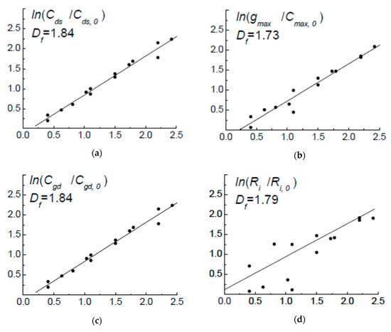
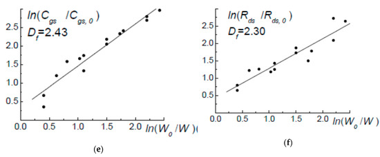
Figure 7.
The linear dependences on ln(W0/W) written in log–log scale: ln(Cds/Cds,0)—(a); ln(Cgd/Cgd,0)—(b); ln(Cgs/Cgs,0)—(c); ln(gmax/gmax,0)—(d); ln(Ri/Ri,0)—(e); ln(Rds/Rds,0)—(f).
According to Figure 7 and Table 2, every subspace SM(Mk,i) of the selections of the parameters Pk,i has its own value DH(f) in the defined ranges. This points out the multifractality of the subspaces SM(Mk,i), characterized by several values DH(f) depending on linear sizes (in our case on n and d). For instance, for the selection 1-1, the range of the Hausdorff dimension DH values of the subspaces of capacities Cds and Cgd measures is 1.79–1.86, of the subspace of capacity Cgs measures it is 2.23–2.59, of the subspace of resistance Rds measures this is 2.15–2.30, and so on. As it is reported in Section 2.2 and below, in this case it is convenient to use average values of the dimensions <DH> for each selection (Table 2, Table 3 and Table 4).
Thus, the average values <DH> = 1.82, 1.87, 1.78 and 1.89 for Cds (Figure 7a) and Cgd (Figure 7b) capacity parameters subspace—close to 2—mean that in spite of the linearity of the channel the law of change of their values is close to the square one. The proximity of the spatial dimension values <DH>(Cds) and <DH>(Cgd) to the spatial dimension value DH = 1.85 of the lateral irregularities of the subsurface potential point out the connection between the geometry of the functional space of the used HES electrophysical characteristics pk,i and the device characteristics of the transistor linear model EC components. The fractal values <DH>(gmax) and <DH>(Ri) of parameter measure subspaces gmax (Figure 7d) and Ri (Figure 7e), which values are also close to <DH> = 1.87, 1.79 and 1.78, behave in the similar way. In such cases, the values <DH> close to 2 are probably defined by the assembly of one-dimensional transistor channels distributed in HES two-dimensional surface—the more n, the closer to two values DH.
The values of the fractal dimensions of the capacity Cgs parameter subspaces (Figure 7c) exceeding 2—<DH>(Cgs) = 2.42, 2.52, 2.37 and 2.39—point out the fact that their physical nature is defined not only by two-dimensional effects, but in some degree also by three-dimensional ones (Table 2). The resistive parameter measure subspaces behave the similar way—<DH>(Rds) = 2.23, 2.26 and 2.43 (Figure 7f). This means that their behavior is also strongly influenced by the third dimension. The DH values proximity to three can be explained by the fact that the Rds and Cgs parameters are defined by flowing 2D-electrons of the HEMT structure channel, not through the 2-dimensional, but through the 3-dimensional (DT = 3) plane, which corresponds to the results represented in [12,30].
Because of the foregoing, it is possible to give the following interpretation of the size effects observed in linear models, and subsequently, in the HF characteristics of AlGaN/GaN HEMT.
The parameter values pk,i of the studied HES electrophysical characteristics in the local approximation have non-linear dependence on linear sizes l and d (e.g., Figure 1b). Subsequently, the parameter values Pk,i = Pk,i(n,d) of the internal transistor EC components defined by them have non-linear dependence on n and d with all that it implies.
Specifically, the dependence of Pk,i = Pk,i(W) on the way of W = n × d obtaining—the variant of comparison—leads to the fact that every such variant of comparison belongs to the individual subspace SM, each of which can be characterized by the own average value <DH> (Table 2, Table 3 and Table 4). The usability of one or another comparison variant depends on the individual case.
Thus, being aware of the corresponding dimension Df(H)(n,d) of the subspace SM and the known values of the measures Mk,0 of the parameters Pk,0 of the initial transistor, from (9) it is possible to reconstruct the values Mk,i belonging to this subspace of the parameters Pk,i of another transistor with some predefined n and d. For example, for the first comparison variant (d = Const):
where Df is fractal dimension of the metric subspace with the measure of the parameter Pk,i. The similar expressions can be written for other comparison variants too. In the expression (21) the relation of electrophysical parameters Pk,i of the HES with the values (measures) of the EC small-signal model parameters Pk,i is realized through the HES fractal dimension (in general case, Hausdorff dimension).
These actions, together with the reconstruction of the values of the desired transistor linear model parameters, lead to obtaining necessary sizes of its structural elements. This significantly speeds up the development, optimization and approbation processes for the HEMTs with predefined device characteristics.
Therefore, the results obtained point out the existence of the similarity phenomenon, not only in HES metric spaces R, but also in corresponding to them functional spaces (metric spaces with the measure SM = {R, Mk}) of their electrophysical characteristic measures, which in the general case is not obvious. At this, the similarity dimensions DS(R) and DS(SM) of subspaces R and SM have the values close enough. Probably, it can reveal the existence of some transformation Π between HES metric space R and the defined on it metric space with the measure SM(pk,i):
In a similar way to (22), it is possible to make another conclusion: there must be a transformation Π* which associates the metric space SM(Pk,i) of linear (or non-linear) transistor model parameters Pk,i with metric space SM(pk,i) of electrophysical parameters pk,i of the transistor’s materials and structural elements (HES structure, ohmic contacts, gates, passivating coatings, connections, etc.):
For example, the transformations Π and Π* can be represented in the form of a physical or mathematical law. Thus, being aware of the spatial dimension of the semiconductor structure geometry and its additive electrophysical characteristics depending on it in local approximation, it is possible to reconstruct, for the individual n and d from the set R, the parameter values of the linear model internal transistor EC components through the transformations Π and Π*. The further investigations are necessary to find out and analyze Π and Π*.
The recently found size effects in the electrical characteristics of ohmic contact [30] and thin-film metallization [42,43,44] point out that in the general case it is necessary to take into account external (parasitic) components of the compact model EC to give a full description of size effects in field-effect transistors. The values of such parasitic components also depend in local approximation on the linear sizes of external transistor structural elements.
The proposed size approach (9) and (21) in most cases gives the opportunity to predict the behavior of fT and fmax depending on n and d, even without using compact models. As it is shown in Table 1, the values fT and fmax calculated from (21) have the best correspondence to the experimental ones. In this case, the cycle of high-frequency oscillations T = 1/f is used as the measure, for it is additive value. Thus, the increase of channel length leads to the increase of the time τ during which electrons pass through it and, consequently, to the growth of the value T. At this, the average values of fractal dimensions <DH(gmax)> are used to calculate fT: 1.87 for the selection 1-1, 1.79 for the selection 1-2, 1.78 for the selection 1-3, 1.46 for the selection 1-4. The average values <DH(Cgs)> are used to calculate fmax: 2.42 for the selection 1-1, 2.52 for the selection 1-2, 2.37 for the selection 1-3, 2.39 for the selection 1-4. The initial values M0 are equal to the experimental values of the oscillation cycles T corresponding to the maximum value W.
In spite of the channel and gate linear geometry (DT = 1), the values <DH> used for cutoff frequency fT and maximum frequency fmax calculation have the average dimension values <DH(Rds)> and <DH(Cgs)> close to two and three, correspondingly (Table 2, Table 3 and Table 4). This fact reveals the strong influence of the two-dimensional effects on fT values (defined by the pattern of linear channels’ distribution in the two-dimensional plane of the transistor) and three-dimensional effects on fmax values (the peculiarities of the scattering 2D-electrons during their motion in three-dimensional plane), that is not obvious.
In addition to this stated above, the results represented in Table 2, Table 3 and Table 4 give the opportunity to find out a geometrical attribute which implies the following: in local approximation the fractal dimension of the studied object can by itself depend on reference coordinates (or point of view) of the observer.
Thus, at HEMT structure optimization by means of selecting section number n, it is necessary to use certain average values <DH> (Table 2 and Table 3), and by means of selecting the values d and W—the other average values (Table 3 and Table 4). This fact can probably point out the existence of some superior attribute of chaotic systems.
The results obtained make it possible to form some hypothesis for the relationship between the measure of the fractal object and the Hausdorff dimension of its space in a local approximation: “If the metric space dimension of the object under investigation depends on the point of view (the state) of the observer, then the measure value (functional) of this object will also depend on the observer’s point of view.” In other words: “In order for the measure (functional) of the object under investigation to depend on the point of view (state) of the observer, it is necessary and sufficient for this object’s metric subspace dimension to depend on the observer’s point of view.”
8. Conclusions
The investigation of size effects manifested themselves in the dependence of AlGaN/GaN HEMT high-frequency characteristics on the channel width d and section number n, was carried out with the use of the notions of measure, metric and normalized functional (linear) spaces, which gave the opportunity to consider scalar and vector values, continuous functions and various numerical sequences from the same point of view.
According to the results obtained, the similarity phenomenon can exist, not only in HES metric spaces, but also in the defined on them functional spaces (metric spaces with a measure) of the measures of their additive electrophysical characteristics and parameter values of internal transistor equivalent circuit components, which is not obvious in the general case. Thereafter, the nature of size effects is in large measure defined by the dependence of AlGaN/GaN HEMT high-frequency characteristics on the scale dependence in local approximation (at l < L) of additive electrophysical properties of the material used for their manufacturing.
In the particular case, the law of mutual transformation of the internal transistor equivalent circuit component parameters belonging to the same functional space determined on R has been found. Thus, being aware of Df(H) and initial values of the measures Mk,0 of the parameters Pk,0 for the initial transistor, it is possible to find out the values Mk,i of the parameters Pk,i of any other transistor made from the same material (with the same value Df(H)) and with predefined n and d. The proposed approach makes it possible, not only to define the sizes of the desired transistor structural elements, but to also reconstruct simultaneously the parameters of its linear (and may be non-linear) model, which significantly speeds up the development, optimization and approbation processes for the HEMT with predefined device characteristics.
If the parameters of the linear model equivalent circuit components belong to the same metric space R, the proposed approach gives an opportunity to predict accurately enough—even without using compact models—the behavior of the cutoff frequencies fT and fmax (and probably H21 and Gmax) depending on n and d.
At transferring to a global approximation (l ≥ L), when topological and fractal dimensions coincide DT = Df, the behavior of HES electrophysical parameters, and consequently, AlGaN/GaN HEMT internal transistor equivalent circuit parameters, as well as their HF characteristics, have linear (classic) dependences upon n and d, which are peculiar to the spaces of integer topological dimensions DT.
Author Contributions
Conceptualization, N.A.T. and L.I.B.; methodology, N.A.T. and A.A.K.; investigation, N.A.T. and A.A.K.; writing—original draft preparation, N.A.T.; writing—review and editing, L.I.B.; supervision, N.A.T.; project administration, L.I.B.
Funding
The project was carried out with financial support of Ministry of Education and Science of the Russian Federation. Unique identifier is 8.3423.2017/4.6.
Conflicts of Interest
The authors declare no conflict of interest.
References
- Aoki, K. Nonlinear Dynamics and Chaos in Semiconductors; British Library Cataloguing-in-Publication Data: London, UK, 2002; p. 580. [Google Scholar]
- Adam, P.M. Fractal Magnetic-Conductance Fluctuations in Mesoscopic Semiconductor Billiards; UK University of New South Wales: Sydney, Australia, 2000; p. 241. [Google Scholar]
- Micolich, A.P.; Taylor, R.P.; Davies, A.G.; Fromhold, T.M.; Linke, H.; Macks, L.D.; Newbury, R.; Ehlert, A.; Tribe, W.R.; Linfield, E.H.; et al. Three key questions on fractal conductance fluctuations: Dynamics, quantization, and coherence. Phys. Rev. 2004, 70, 085302. [Google Scholar] [CrossRef]
- Torkhov, N.A. Fractality as a new nanotechnological direction of semiconductor material science. In Proceedings of the 24th International Crimean Conference “Microwave and Telecommunication Technology”, Sevastopol, Russia, 8–13 September 2014. [Google Scholar]
- Rekhviashvili, S.S.; Mamchuev, M.O.; Mamchuev, M.O. Model of Diffusion-Drift Charge Carrier Transport in Layers with a Fractal Structure. Phys. Solid State 2016, 58, 788–791. [Google Scholar] [CrossRef]
- Barnsley, M.F. Superfractals; Cambridge University Press: London, UK, 2006. [Google Scholar]
- Feder, J. Fractals; M. Mir: Moscow, Russia, 1991; p. 261. [Google Scholar]
- Torkhov, N.A. Formation of a Native-Oxide Structure on the Surface of n-GaAs under Natural Oxidation in Air. Semiconductors 2003, 37, 1205–1213. [Google Scholar] [CrossRef]
- Torkhov, N.A. Method for determining the values of fractal sizes of interfaces. J. Surf. Investig. 2010, 52–67. [Google Scholar]
- Shmidt, N.M.; Emtsev, V.V.; Kolmakov, A.G.; Kryzhanovsky, A.D.; Lundin, W.V.; Poloskin, D.S.; Ratnikov, V.V.; Titkov, A.N.; Usikov, A.S.; Zavarin, E.E. Correlation of mosaic-structurepeculiarities with electric characteristicsand surface multifractal parameters for GaN epitaxial layers. Nanotechnology 2001, 12, 471–474. [Google Scholar] [CrossRef]
- Shmidt, N.M.; Aliev, G.; Besyul’kin, A.N.; Davies, J.; Dunaevsky, M.S.; Kolmakov, A.G.; Loskutov, A.V.; Lundin, W.V.; Sakharov, A.V.; Usikov, A.S.; et al. Mosaic Structure and Optical Properties of III–Nitrides. Phys. Status Solidi 2002, 1, 558–562. [Google Scholar] [CrossRef]
- Torkhov, N.A.; Babak, L.I.; Kokolov, A.A.; Salnikov, A.S.; Dobush, I.M.; Novikov, V.A.; Ivonin, I.V. Nature of size effects in compact models of field effect transistors. J. Appl. Phys. 2016, 119, 094505. [Google Scholar] [CrossRef]
- Mokerov, V.G.; Kuznetsov, A.L.; Fedorov, Y.V.; Bugaev, A.S.; Pavlov, A.Y. AlGaN/GaN-HEMTs with a breakdown voltage higher than 100 v and maximum oscillation frequency fmax as high as 100 GHz. Semiconductors 2009, 43, 537–543. [Google Scholar] [CrossRef]
- Palacios, D.Y.; Chakraborty, A.; Sanabria, C.; Keller, S.; DenBaars, S.P.; Mishra, U.K. Optimization of AlGaN/GaN HEMTs for high frequency operation. Phys. Status Solidi 2006, 203, 1845–1850. [Google Scholar] [CrossRef]
- Jacobs, B.; Karouta, F.; Kwaspen, J.J.M. The processing and scalability of AlGaN/GaN HEMTs. In Proceedings of the Conference GaAs-99, Munich, Germany, 4–5 October 1999. [Google Scholar]
- Pretet, J.; Subba, N.; Ioannou, D.; Cristoloveanu, S.; Maszara, W.; Raynaud, C. Channel-width dependence of floating body effects in sti- and LOCOS-isolated MOSFETS. Microelectron. Eng. 2001, 59, 483–488. [Google Scholar] [CrossRef]
- Kolmogorov, A.N.; Fomin, S.V. Elements of the Theory of Functions and Functional Analysis, 4th ed.; Nauka: Moscow, Russia, 1976. [Google Scholar]
- Poinkaré, A. On the Dynamics of the Electron. In Principle of Relativity: Polygraph of Relativism Classics; Atomizdat: Moscow, Russia, 1973; p. 90. [Google Scholar]
- Ivanishko, I.A.; Krotov, V.G. Compactness of Embeddings of Sobolev Typeon Metric Measure Spaces. Math. Notes 2009, 86, 775–788. [Google Scholar] [CrossRef]
- Gelfand, I.M.; Fomin, S.V. Calculus of Variations; State Publishing House of Physico-Mathematical Literature: Moscow, Russia, 1961; p. 220. [Google Scholar]
- Tikhonov, Y.V. Extended Abstract of Dissertation for the Candidate of Physical and Mathematical Sciences Degree. In Classes of Singular Functions in Various Functional Spaces; Lomonosov Moscow State University: Moscow, Russia, 2016. [Google Scholar]
- Barnsley, M. Fractals Everywhere; Academic Press: New York, NY, USA, 1988. [Google Scholar]
- Nazarov, A.I.; Nikitin, Y.Y. Logarithmic L2-small ball asymptotics for some fractional gaussian processes. Soc. Ind. Appl. Math. 2004, 49, 645–658. [Google Scholar] [CrossRef]
- Torkhov, N.A.; Bozhkov, V.G.; Ivonin, I.V.; Novikov, V.A. Determination of the Fractal Dimension for the Epitaxial n-GaAs Surface in the Local Limit. Semiconductors 2009, 43, 33–41. [Google Scholar] [CrossRef]
- Jeon, M.Y.; Kim, B.G.; Jeon, Y.J.; Jeong, Y.H. A Technique for Extracting Small-Signal Equivalent-Circuit Elements of HEMTs. IEICE Trans. Electron 1999, 82, 1968–1976. [Google Scholar]
- Dambrine, G.; Cappy, A.; Heliodore, F.; Playez, E. A new method for determining the FET small-signal equivalent circuit. IEEE Trans. Microw. Theory Tech. 1988, 36, 1968–1976. [Google Scholar] [CrossRef]
- Materka, A.; Kacprzak, T. Computer calculations of large-signal GaAs FET amplifier characteristic. IEEE Trans. Microw. Theory Tech. 1985, 33, 129. [Google Scholar] [CrossRef]
- Torkhov, N.A.; Bozhkov, V.G. Fractal nature of the resistance of the drain-source channel of a GaN heterostructure of a field-effect transistor with a two-dimensional electron gas. In Proceedings of the 20th International Crimean Conference “Microwave and Telecommunication Technology”, Sevastopol, Ukraine, 13–17 September 2010; pp. 729–730. [Google Scholar]
- Mironov, V.L. The Basic Principles of Scanning Probe Microscopy; Institute of Physics of Microstructures, RAS: Nizhny Novgorod, Russia, 2004; p. 114. [Google Scholar]
- Torkhov, N.A.; Bozhkov, V.G. The effect of the linear dimensions of the drain-source channel of the arsenide-gallium PTSh on its static current-voltage characteristics (lateral size effect). In Proceedings of the 21th International Crimean Conference “Microwave and Telecommunication Technology”, Sevastopol, Russia, 12–16 September 2011. [Google Scholar]
- Torkhov, N.A.; Bozhkov, V.G.; Zhuravlev, K.S.; Toropov, A.I. The effect of the fractal nature of the distribution of ionized shallow donor impurities on the resistivity of the active layer of the field-effect transistor structure. In Proceedings of the 20th International Crimean Conference “Microwave and Telecommunication Technology”, Sevastopol, Russia, 13–17 September 2010. [Google Scholar]
- Torkhov, N.A.; Bozhkov, V.G. Fractal Character of the Distribution of Surface Potential Irregularities in Epitaxial n-GaAs (100). Semiconductors 2009, 43, 551–556. [Google Scholar] [CrossRef]
- Reiner, R.; Waltereit, P.; Benkhelifa, F.; Müller, S.; Walcher, H.; Wagner, S.; Quay, R.; Schlechtweg, M.; Ambacher, O. Fractal structures for low-resistance large area AlGaN/GaN power transistors. In Proceedings of the 24th International Symposium on Power Semiconductor Devices and ICs, Bruges, Belgium, 3–7 June 2012. [Google Scholar]
- Torkhov, N.A.; Salnikov, A.S.; Bozhkov, V.G.; Babak, L.I.; Dobush, I.M. Size effect in linear GaN HEMT Ka-band models. In Proceedings of the 24th International Crimean Conference “Microwave and Telecommunication Technology”, Sevastopol, Russia, 8–13 September 2014; pp. 133–134. [Google Scholar]
- Hayden, L. An Enhanced Line-Reflect-Reflect-Match Calibration. In Proceedings of the 67th ARFTG Conference, San Francisco, CA, USA, 16 June 2006. [Google Scholar]
- Kokolov, A.A.; Babak, L.I. Methodology of built and verification of non-linear EEHEMT model for GaN HEMT transistor. Radioelectron. Commun. Syst. 2015, 58, 435–443. [Google Scholar] [CrossRef]
- Berroth, M.; Bosch, R. Broad-Band Determination of the FET Small-Signal Equivalent Circuit. IEEE Trans. Microw. Theory Tech. 1990, 38, 891–895. [Google Scholar] [CrossRef]
- Shirakawa, K.; Oikawa, H.; Shimura, T.; Kawasaki, T.; Ohashi, Y.; Saito, T.; Daido, Y. A n Approach to Determining an Equivalent Circuit for HEMT’s. IEEE Trans. Microw. Theory Tech. 1995, 43, 499–503. [Google Scholar] [CrossRef]
- Ooi, B.L.; Zhong, Z.; Leong, M.S. Analytical Extraction of Extrinsic and Intrinsic FET parameters. IEEE Trans. Microw. Theory Tech. 2009, 57, 254–261. [Google Scholar]
- Kokolov, A.A.; Babak, L.I. A New Analytical Technique for Extraction of Bias-Dependent Drain Resistance in GaAs and GaN HEMTs. Microw. Opt. Technol. Lett. 2015, 57, 2536–2539. [Google Scholar] [CrossRef]
- Goryainov, A.E.; Stepacheva, A.V.; Dobush, I.M.; Babak, L.I. Software Module for Extracting Models of Passive Components of Microwave Monolithic Integrated Circuits Based on the Indesys-MS Environment. In The Collection of Scientific Papers: Contemporary Issues of Radioelectronics; TUSUR: Tomsk, Russia, 2016; pp. 312–318. [Google Scholar]
- Torkhov, N.A.; Novikov, V.A. Fractal geometry of the surface potential in electrochemically deposited platinum and palladium films. Semiconductors 2009, 43, 1071–1077. [Google Scholar] [CrossRef]
- Torkhov, N.A.; Bozhkov, V.G.; Novikov, V.A.; Zemskova, N.V.; Burmistrova, V.A. The effect of various treatments on the fractal nature of the surface topography of gallium arsenide. J. Surf. Investig. 2011, 5, 75–89. [Google Scholar]
- Torkhov, N.A. Sheet Resistance of the TiAlNiAu Thin-Film Metallization of Ohmic Contacts to Nitride. Surfaces. Interfaces Thin Films 2019, 53, 28–36. [Google Scholar]
© 2019 by the authors. Licensee MDPI, Basel, Switzerland. This article is an open access article distributed under the terms and conditions of the Creative Commons Attribution (CC BY) license (http://creativecommons.org/licenses/by/4.0/).