Article

Tunable Control of Mie Resonances Based on Hybrid VO2 and Dielectric Metamaterial

1
School of Electronic and Communication Engineering, Harbin Institute of Technology, Harbin 150001, China
2
Department of Information and Telecommunication Engineering, Incheon National University, Songdo-1-dong, Yonsu-gu, Incheon 210211, Korea
*
Author to whom correspondence should be addressed.
Symmetry 2018, 10(10), 423; https://doi.org/10.3390/sym10100423
Submission received: 3 September 2018 / Revised: 15 September 2018 / Accepted: 17 September 2018 / Published: 20 September 2018

Abstract

:
In this paper, a tunable dielectric metamaterial absorber with temperature-based vanadium dioxide (VO2) is proposed. In contrast to previous studies, both the metal phase of VO2 and the semiconductor phase are applied to manipulate the Mie resonant modes in the dielectric cubes. By embedding VO2 in the main resonant structure, the control over Mie resonant modes in dielectric metamaterials is realized. Each resonant mode is analyzed through field distribution and explains why the phase switch of VO2 could affect the absorbance spectrum. This use of tunable materials could create another new methodology for the manipulation of the Mie resonance-based dielectric cubes and make them closer in essence to isotropic metamaterials.

1. Introduction

The study of electromagnetic waves began in the late 1800s. Over the course of a century’s research, the primary goal modern electromagnetic wave research has been to achieve full control of it, including amplitude control, phase control, and wave impendence control [1,2,3,4,5]. Dielectric composites have been proposed for many applications, and exhibit excellent absorption properties, while the electric resonant mode and magnetic resonant mode overlap with each other [6,7,8,9,10,11]. Some papers have also proposed tunable metamaterial and metasurface absorbers based on graphene [12,13,14,15] or strontium titanate [16,17] to realize tunable absorption or anomalous refraction. Frequency-stable and continuously tunable performance could be achieved by varying the voltage or temperature.
Vanadium dioxide (VO2) has drawn a great deal of interest for its semiconductor-to-metal transition and low transition temperature (68 °C) [18,19,20]. Another characteristic that makes VO2 a promising tunable material is that the switching time is very fast when changing from a semiconductor property to a metal property. The study of VO2 is mainly focused on two areas: the first design idea is changing the electrical length by exploiting the ultra-large change of the refractive index in VO2 between the semiconductor and the metallic states [21,22,23], and the second design idea is changing the transverse electric and transverse magnetic pass with different phases [24,25]. However, these two ideas are still far from achieving full control over the electromagnetic wave.
In this paper, a tunable dielectric metamaterial absorber with vanadium dioxide is proposed. Unlike previous papers, which only take advantage of the metal properties of VO2 and change the electrical length of the structure, this paper makes use of both material properties to control the absorption. The basic absorber is a cross-shaped high permittivity ceramic, and VO2 is placed first in the center and then on the edge of this absorber to achieve the tunability of the absorption. The resulting composite material functions as a sub-wavelength metamaterial with the tunable operating material phase permitting the realization of an absorber.

2. Modeling and Design Principle
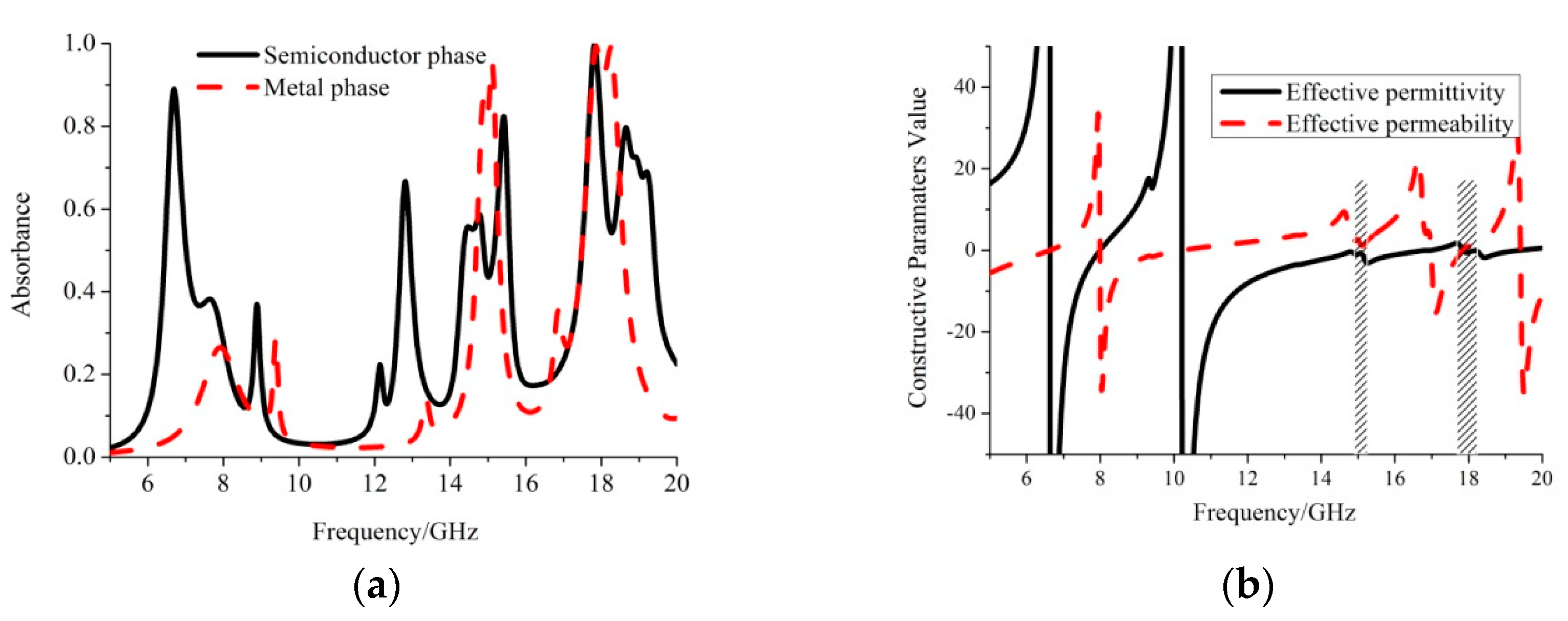
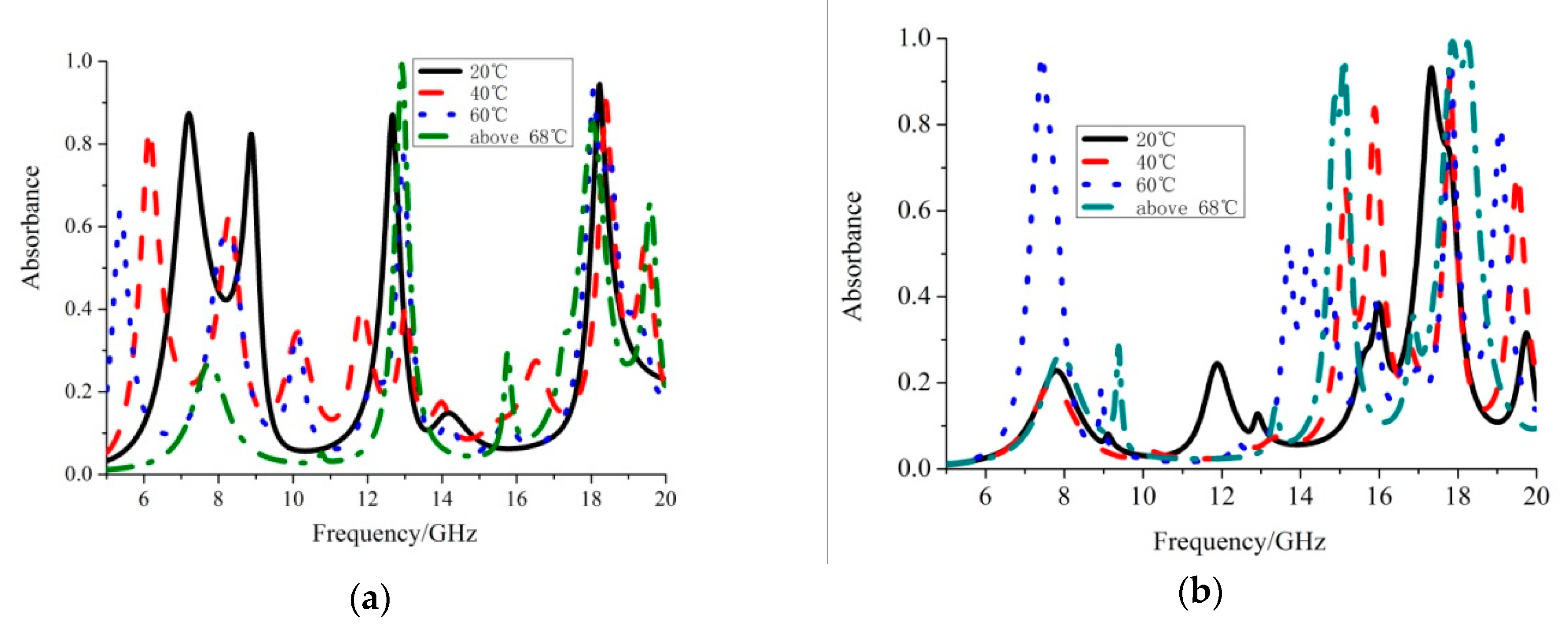
This study starts with the cross-shaped dielectric metamaterial absorption. For metamaterial or metasurface absorbers, one of the most important conditions is the exploitation of epsilon-near-zero (ENZ) materials [26]. A cross-shaped absorber was developed from the cube absorber [27]. By adding other components into the unit cell, ENZ materials can be obtained by the Mie resonances inside the cross-shaped structure.
First, this study starts with the Mie resonance inside the dielectric cube. The incident wave excites different Mie resonant modes at different frequencies. As there are different application requirements, full control over the resonant modes is needed. Learning from the broadband antenna or left-handed metamaterial design, adding some other structures into the unit cell could manipulate the resonant modes by tuning the nearby resonances together. Based on previous experience with absorbers, the cross-shaped dielectric absorber could have three absorbance peaks corresponding to three resonant frequencies and resonant modes. At each resonant frequency, the incident energy is trapped in the center of the shape and both dielectric arms, on the basis of the electric wave. This multi-mode resonance structure has great advantages in wave control, and also makes it easier to accomplish different electromagnetic goals. Compared to the similar shapes [28,29], the cross-shaped absorber can also be regarded as a complementary dielectric cube absorber. Based on the equivalent circuit theory, the cross-shaped structure is smaller while keeping the same resonant performance. Additionally, the unit cell is composed of dielectric ceramics, which means low ohmic loss and a greater suitability for high-temperature and high-power conditions. Considering that temperature is one of the most important parameters in this study, it is necessary to keep the host unit cell shape and constitutive parameters stable while tuning the temperature. Therefore, the cross shape is the best candidate for the study of a hybrid VO2 and dielectric metamaterial absorber.
By replacing the ceramic into the vanadium dioxide at the energy-concentrated positions, a tunable absorber is achieved with a different material phase of vanadium dioxide. The VO2-dielectric absorber unit cell is shown in Figure 1.

2.1. Center Case

In the cross-shaped dielectric metamaterial absorber, one of the resonant modes concentrates on the incident energy around the center of the cross shape. Consequently, in the first case, the effect of the material phase on absorption is discussed by replacing the center material with VO2. The material properties used in this paper are based on the results published before [7]. In this first case, the dielectric arms of the cross-shaped absorber are connected directly with each other without VO2. The simulated results of the different VO2 phase absorptions are shown in Figure 2.
The constitutive parameters are calculated by the following formulas:
μ e f f = n Z = 1 k 0 d ( 1 + S 11 ) 2 S 21 2 ( 1 S 11 ) 2 S 21 2 [ Im ( ln 1 Re S 11 S 21 ) i Re ( ln 1 Re S 11 S 21 ) ] ,
ε e f f = n / Z = 1 k 0 d [ Im ( ln 1 Re S 11 S 21 ) i Re ( ln 1 Re S 11 S 21 ) ] ( 1 + S 11 ) 2 S 21 2 ( 1 S 11 ) 2 S 21 2 .
Figure 2a shows the different absorbance results achieved through the different VO2 material phases. The red dotted line shows the absorption of the dielectric metamaterial while VO2 operates as a metal. Under this condition, three main resonant peaks and two slight resonant peaks were observed. The main resonant peak appeared at 12.92 GHz and the resonant absorption was 99.3%. The other two main resonant peaks appeared around 18.04 GHz and 19.59 GHz, and the absorptions were 85.2% and 65.6%, respectively. Each of these resonant peaks corresponds to a resonant mode, and the underlying mechanism of the proposed tunable dielectric metamaterial absorber was the modification of the resonant mode and resonant frequency while controlling the material phase of VO2. The other two slight resonant peaks were around 7.79 GHz and 15.79 GHz.
The black solid line shows the absorption of the dielectric metamaterial absorber while VO2 operates under a semiconductor phase. In this condition, the dielectric metamaterial absorber was composed of two different permittivity dielectric cubes, and excited several orders of Mie resonant modes inside the cubes. Figure 2 shows that the absorption over the whole frequency band was more complicated when VO2 operated under a semiconductor phase. There were four main resonant peaks which could keep the absorption over 80% at 8.11 GHz, 12.43 GHz, 12.84 GHz, and 18.34 GHz, respectively. When the VO2 phase changed from metal to semiconductor, the first resonant mode was enhanced. This means that the absorbance efficiency was improved to as high as 91.8% without a frequency shift. Another resonant enhancement occurred at 16.62 GHz. At this resonant mode, the VO2 phase switching led to a resonant frequency which shifted from 15.79 GHz to 16.61 GHz, and the absorbance efficiency was enhanced from 27.3% to 68.2%.
At the second main resonant frequency of the semiconductor-phase dielectric absorber, the resonance reached around 12.45 GHz and was nearly combined with the third resonance, which was around 12.84 GHz. Unlike that of the metal phase, the resonant mode of this resonance split into two. Also unlike the metal phase, by modifying the electromagnetic field of the semiconductor cube at the center, Mie resonance was excited inside the cube rather than through reflection. Therefore, the dielectric absorber generated another resonant mode and shifted the resonant frequency. The resonant intensity decreased while the resonant mode split into two independent modes.
The last main resonant frequency at 18.34 GHz was enhanced from the third resonant frequency in the metal phase. Meanwhile, the resonant intensity was also increased and shifted to a higher resonant mode nearby. The field distribution of the dielectric metamaterial absorber with VO2 in both the metal and semiconductor phases is shown in next section. The incident electric field vector is along the Y-axis.
Figure 2b shows the effective constitutive parameters of the dielectric metamaterial while VO2 operated in the metal phase. The metamaterial absorber showed either negative permittivity or a permeability of 5 GHz to 12 GHz, so the incident wave was reflected over these frequency bands, which is also verified in Figure 2a. The dashed areas in Figure 2b show that the effective permittivity and permeability both approximated to zero. This means the absorber operated as a double-zero metamaterial at these two dashed areas in Figure 2b, corresponding to the best absorption performance around 12.92 GHz and 18.04 GHz, shown in Figure 2a.

2.2. Dielectric Arm Case

The resonance of traditional cross-shaped dielectric metamaterial absorbers mainly focuses the incident energy on either the shape center or the dielectric arm. Therefore, the tunable material placed in the dielectric arm was investigated in this part of study. The absorbance of the dielectric absorber with VO2 in the dielectric arm is shown in Figure 3.
The black solid line in Figure 3 represents the absorbance of the dielectric absorber when VO2 operates as a semiconductor in the dielectric arm. There were four main resonant frequencies in this case, with four main resonant frequency bands around 6.71 GHz, 12.89 GHz, 15.41 GHz, and 17.83 GHz. The best absorbance efficiency was 99.97% when the absorber operated at 17.83 GHz. The electric and magnetic field distributions at these four main resonant frequencies are shown in next section.
The red dotted line in Figure 3 shows the absorbance when the temperature was above 68 °C and VO2 operated as a metal. Comparing the absorption to when VO2 is a semiconductor, the material phase switch suppressed the resonance to around 6.71 GHz and 12.89 GHz. This is because the main resonant part is the semiconductor plate in the dielectric arm, which means that these two resonant modes are evanescent after the material phase switches. There were two main resonant peaks of the red dotted line around 14.88 GHz and 17.88 GHz. The absorbance at these two frequencies was 86.4% and 99.1%, respectively.
Figure 3b shows the effective constitutive parameters when VO2 operated as a metal phase in the dielectric arms. Similar to the first case, the metamaterial absorber showed double-zero characteristics at the resonant frequencies. It is therefore important to excite a double-zero electromagnetic response in the design of a metamaterial absorber. The double-zero areas in Figure 3b are shown in shaded.

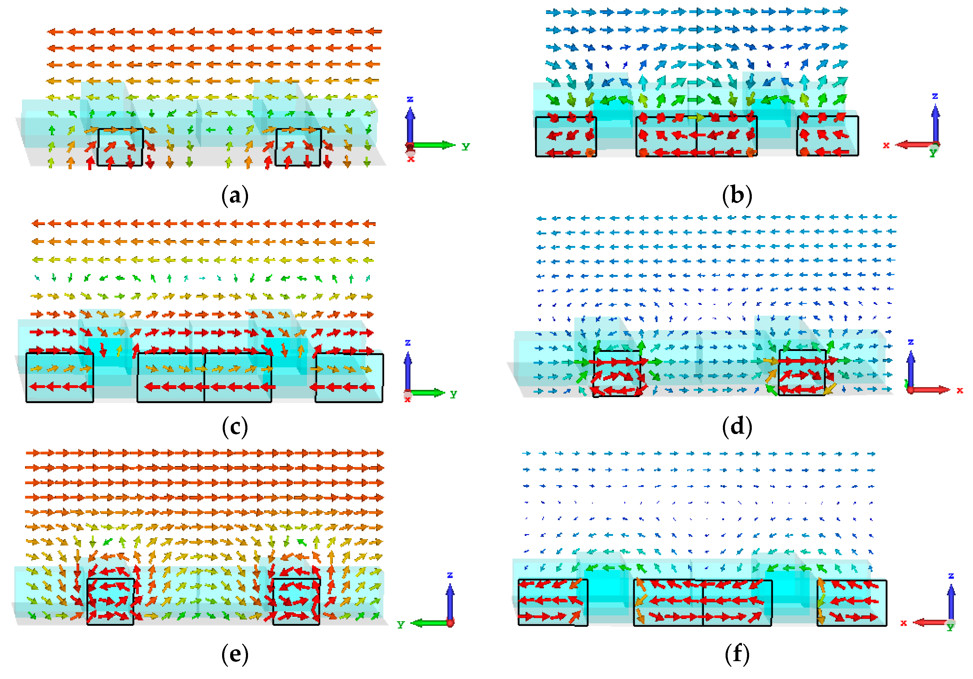
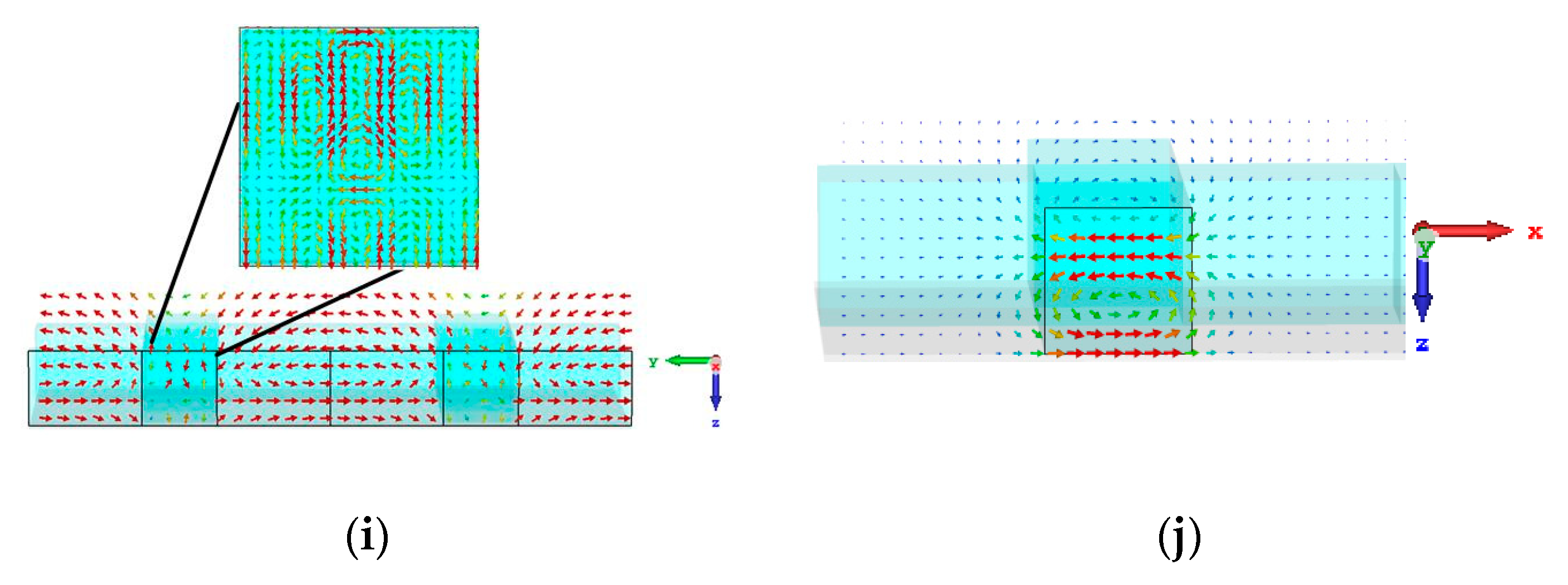
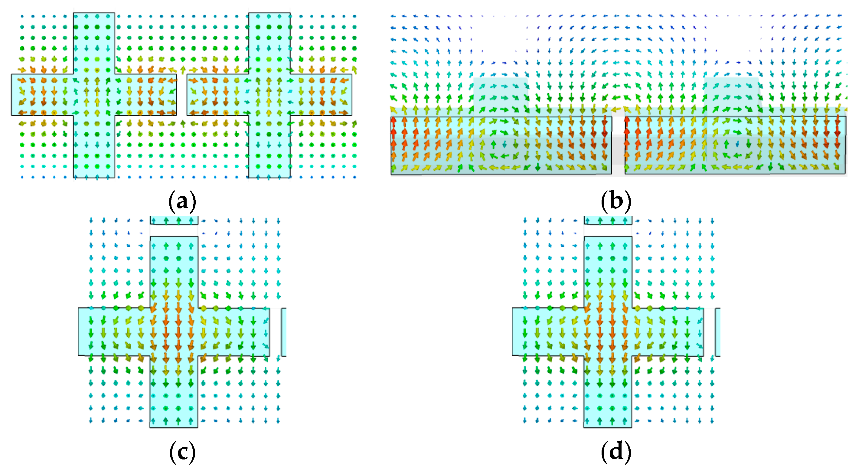
3. Tunable Mechanism Illustration through Field Distribution

Tunable performance was achieved through material phase switching. By demonstrating the electric and magnetic field distributions over resonant frequencies, the physical mechanism inside the VO2-dielectric metamaterial absorber is illustrated.

3.1. Center Case

Figure 4 shows the field distribution at each resonant frequency while the temperature is above 68 °C and VO2 operates as a metal phase. Figure 4a,b shows that most of the incident wave was concentrated in the dielectric arm along the X-axis. The incident electric field is along the Y-axis, and at a resonant frequency of 12.92 GHz the incident electric wave was converted to form a circular field distribution, resulting in a magnetic field enhancement in the dielectric arm which can also be verified in Figure 4b. This resonant mode can therefore be regarded as a magnetic dipole, and this is a magnetic resonant mode.
In Figure 4c,d, the resonant frequency increased to 18.04 GHz. At this frequency, the incident magnetic field was converted to form a circularly field distribution in the dielectric arm along the Y-axis, resulting in the enhancement of the electric field. The dielectric absorber can therefore be regarded as an electric dipole at this resonant frequency, and this resonant mode is an electric mode. The incident energy was contained in the dielectric arm and reduced to a lower energy level.
The higher Mie resonance mode in the dielectric absorber can be observed in Figure 4e,f. These two figures show the electric and magnetic field distribution at 19.6 GHz. In this resonant mode, both the electric and magnetic field were circularly distributed, so this absorption peak resulted in a quadrupole-like resonant. However, the absorption at this frequency was not over 80% because this frequency corresponds to a higher resonant mode in the dielectric absorber, and the resonant intensity was not that strong. It is not difficult to see that all these resonant modes were excited in the dielectric arm along the X-axis or Y-axis instead of at the center of the cross shape. This can be explained by the phase of VO2. When VO2 operates as a metal, it prevents the electromagnetic field from forming normal Mie resonance modes. In this case, all the resonance concentrated in the center is suppressed and the resonance within the dielectric arm is enhanced. From this point of view, the basic mechanism of the tunable dielectric VO2 metamaterial absorber lies in the suppression and enhancement of Mie resonant modes in the high-permittivity dielectric cubes.
Figure 5 shows the electric and magnetic field distributions with VO2 operating as a semiconductor at the center of the dielectric absorber. Figure 5a,b,g,h correspond to the field distributions at 8.11 GHz and 16.6 GHz, respectively. Neither of these resonant frequencies were strong enough when VO2 operated as a metal (the two slight resonant modes at 7.79 GHz and 15.79 GHz). The metal phase VO2 prevented the field distribution from the center of the cross shape, so all the resonances were excited in the dielectric arm. As the temperature decreased, VO2 turned into a semiconductor. The phase transformation allowed the electromagnetic field to excite in the cross-shaped center and enhanced its resonance. This greatly increased the absorption across these frequency bands. Both resonances at 8.11 GHz and 16.6 GHz generated a strong resonant and higher resonant mode in the center of the cross shape. There were also 0.32 GHz and 0.81 GHz frequency shifts towards a higher-frequency band accompanying the VO2 phase switching.
The first resonant frequency was 12.92 GHz when the VO2 phase was a metal. This resonant mode split into two resonant modes when the VO2 phase switched from metal to semiconductor. The field distribution of these two resonant modes can be seen in Figure 5c–f. Comparing Figure 5c,e to Figure 4a, it is clear that the electric field distribution did not change very much. The field remained concentrated in the dielectric arm along the X-axis while VO2 switched phase. We can therefore conclude that these two resonant frequencies in the semiconductor VO2 phase split from the resonant frequency at 12.92 GHz when VO2 was in the metal phase. Additionally, comparing Figure 5d,f to Figure 4b, the material phase had a great impact on the magnetic field distribution in the center of the cross shape. The magnetic field distribution at 12.43 GHz and 12.84 GHz was formed by the reflection of the metal ground plane and the incident wave. Additionally, the field distribution in the center was anisotropic along the Z-axis when affected by the dielectric arm resonant. This is why the magnetic field presented several circles at these two resonant frequencies. The initial resonance also split into two resonant modes, and the resonant intensity as well as the absorbance were decreased at these two frequencies.
The field distribution shown in Figure 5i,j was at the same resonant mode as the one shown in Figure 4d,e but with different VO2 material phases. The electric field in the dielectric arm remained firm to keep this resonant mode an electric mode while changing the VO2 phase from metal to semiconductor, but generated another resonant in the cross-shaped center at the same time. As also displayed with frequencies 12.43 GHz and 12.84 GHz, this resonant mode was formed by the incident wave, the reflection from the ground plane, and the influence from the dielectric arm. The absorption increased at this frequency because another resonant was excited at the cross-shaped center. This ensured that the resonant was strong enough to keep the absorbance efficiency.

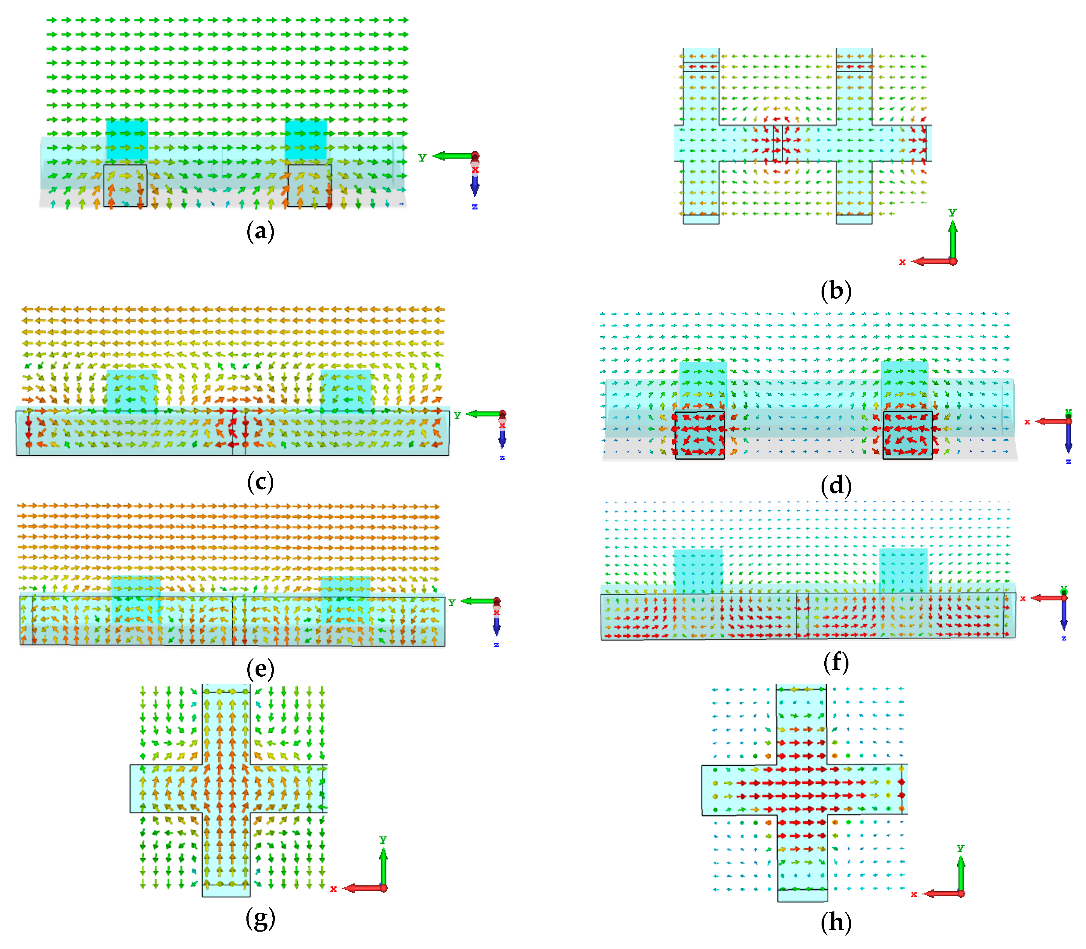
3.2. Dielectric Arm Case

Figure 6 shows the electric and magnetic field distribution at different frequencies. Figure 6a,b respectively show the electric and magnetic field distributions at 6.71 GHz. The excited electric field formed a circular distribution in the dielectric arm along the X-axis. In Figure 6b, it is clearly shown that most of the incident wave was concentrated in the semiconductor VO2 plate. In Figure 6a, the electric distribution showed a higher resonant intensity in the dielectric cube near the ground plane than in the part near air. Thereby, most incident energy was transformed into a lower energy level in the bottom of VO2 at this resonant mode. Just as when the resonant was at 6.71 GHz, the resonant at 12.89 GHz was also gathering the incident energy in the semiconductor VO2 plate, as shown in Figure 6c,d. The difference is that the absorption occurred in the whole VO2 plate at 12.89 GHz instead of only around the bottom.
Figure 6e,f show the electric and magnetic field distributions at 15.41 GHz. In this resonant mode, the incident energy was no longer completely concentrated in the semiconductor VO2 plate. The cross-shaped center and the distance between the center and the plate also played important roles in the absorption. The VO2 phase did have an impact on this resonant mode, but this impact was not as strong as in the first two resonant modes. In the last resonant mode at 17.83 GHz, all of the incident wave vector was converted and formed a circle in the cross-shaped center, as shown in Figure 6g,h. This resonant mode is completely independent from the dielectric arm, so the phase of VO2 had little effect.
Figure 7 shows the electric and magnetic field distributions of a dielectric metamaterial absorber with VO2 in the cross-shaped arm at the two main resonant frequencies of 14.88 GHz and 17.88 GHz. At a frequency of 14.88 GHz, the field distribution was composed of two parts: one in the cross-shaped center, and the other around the VO2 plate. This resonant was therefore affected by the VO2 phase. This can also be confirmed from the absorbance efficiency line. When VO2 transformed from a semiconductor into a metal, the resonant mode around 15.41 GHz decreased to 14.88 GHz, and the absorbance efficiency was increased from 82.3% to 86.4%. In Figure 7c,d the field distribution was fully concentrated in the cross-shaped center, and there was no effect when the VO2 phase switched. This result can also be confirmed by the absorbance efficiency line.
Figure 8 shows the absorption results of the structure tuned by varying temperatures. VO2 operates as a semiconductor when the temperature is lower than 68 °C and presents different dielectric permittivity with different temperatures. The VO2 material properties used in this paper were adopted from Wu work group [20]. When the temperature is above 68 °C, VO2 presents as a metal. The material property of VO2 changes gradually when the temperature increases towards 68 °C. The effect that material property has on absorption can therefore be observed by equally dividing the temperature into three curves before it reaches 68 °C. This method guarantees a clear explanation while keeping the figure distinguishable. Therefore, the tunable performance was observed at 20 °C, 40 °C, 60 °C, and above 68 °C.
Figure 8a shows the absorption when VO2 was placed in the cross-shaped center. When VO2 operated as a semiconductor phase, the absorption frequency was decreased when the temperature increased. Temperature affected the first resonance the most. The first resonant frequency shifted to the left by 1.48 GHz when the temperature increased from 20 to 60 °C. When the temperature was low, some of the resonances in the dielectric absorber were not excited because of the low dielectric permittivity. With increased temperature, the dielectric absorber also excited new resonant modes. As the temperature continued to increase, VO2 changed its material phase into metal and suppressed the resonance within. Figure 8b shows that the same performance could also be observed when VO2 was placed in the dielectric arm. The resonance around 7.44 GHz was excited at 60 °C when the dielectric permittivity was high enough, and was subsequently suppressed once the temperature rose above 68 °C. As the resonances were all excited in the higher frequency band, continuous frequency absorption was achieved when the temperature increased from 20 to 68 °C.
Dielectric metamaterial absorbers based on Mie resonance have a wide range of applications, such as telecommunications, nanoelectronics, antennas, and automotives [30,31,32], all of which require multiple operating bands. The hybrid VO2 and dielectric metamaterial can easily tune the operating band stably and with high efficiency. By tuning the VO2 material phase, the Mie resonance manipulation method proposed here can be an excellent candidate for absorption control in these applications.

4. Conclusions

In this paper, a tunable dielectric metamaterial absorber with temperature-based VO2 is proposed and simulated. By combining VO2 with traditional dielectric cubes, multiple control methods can be applied in the Mie resonances, including the suppression and enhancement of the Mie resonance intensity, as well as the offsetting and splitting of the resonant frequency, and also the combination of different frequencies nearby. The metal phase of VO2 has a strong inhibitory effect on the dielectric resonance at its location. These regulation methods over dielectric metamaterials proposed in this paper can be used not only in absorber design, but also in any other Mie resonant-based dielectric metamaterial. In this study, the Mie resonance manipulation method based on VO2 phase change did not realize wideband absorption due to the isolation of resonant modes. This tuning method could be applied in tandem with equivalent circuit model theory in future studies to overcome the resonant modes isolation in the dielectric materials.

Author Contributions

Conceptualization, K.Z. and Q.W.; methodology, J.G.; software, J.G.; investigation, J.G.; writing–original draft preparation, J.G.; writing–review and editing, K.Z., G.Y., S.K. and Q.W.

Funding

This research was funded by the National Natural Science Foundation of China [No. 61371044 and 61571155].

Acknowledgments

The authors would like to thank the anonymous reviewers and editors for their helpful and constructive suggestions that improved this paper.

Conflicts of Interest

The authors declare no conflict of interest.

References

  1. Stranks, S.D.; Eperon, G.E.; Grancini, G.; Menelaou, C.; Alcocer, M.J.; Leijtens, T.; Snaith, H.J. Electron-hole diffusion lengths exceeding 1 micrometer in an organometal trihalide perovskite absorber. Science 2013, 342, 341–344. [Google Scholar] [CrossRef] [PubMed]
  2. Landy, N.I.; Sajuyigbe, S.; Mock, J.J.; Smith, D.R.; Padilla, W.J. Perfect metamaterial absorber. Phys. Rev. Lett. 2008, 100, 207402. [Google Scholar] [CrossRef] [PubMed]
  3. Low, T.; Avouris, P. Graphene plasmonics for terahertz to mid-infrared applications. ACS Nano 2014, 8, 1086–1101. [Google Scholar] [CrossRef] [PubMed]
  4. Liu, M.; Yang, Q.; Xu, Q.; Chen, X.; Tian, Z.; Gu, J.; Zhang, W. Tailoring mode interference in plasmon-induced transparency metamaterials. J. Phys. D Appl. Phys. 2018, 51, 174005. [Google Scholar] [CrossRef] [Green Version]
  5. Glybovski, S.B.; Tretyakov, S.A.; Belov, P.A.; Kivshar, Y.S.; Simovski, C.R. Metasurfaces: From microwaves to visible. Phys. Rep. 2016, 634, 1–72. [Google Scholar]
  6. Liu, X.; Fan, K.; Shadrivov, I.V.; Padilla, W.J. Experimental realization of a terahertz all-dielectric metasurface absorber. Opt. Express 2017, 25, 191–201. [Google Scholar] [CrossRef] [PubMed]
  7. Zhao, Y.T.; Wu, B.; Huang, B.J.; Cheng, Q. Switchable broadband terahertz absorber/reflector enabled by hybrid graphene-gold metasurface. Opt. Express 2017, 25, 7161–7169. [Google Scholar] [CrossRef] [PubMed]
  8. Fan, K.; Suen, J.Y.; Liu, X.; Padilla, W.J. All-dielectric metasurface absorbers for uncooled terahertz imaging. Optica 2017, 4, 601–604. [Google Scholar] [CrossRef]
  9. Lu, T.; Zhang, D.; Qiu, P.; Lian, J.; Jing, M.; Yu, B.; Wen, J. Ultrathin terahertz dual-band perfect metamaterial absorber using asymmetric double-split rings resonator. Symmetry 2018, 10, 293. [Google Scholar] [CrossRef]
  10. Ye, L.; Chen, X.; Cai, G.; Zhu, J.; Liu, N.; Liu, Q. Electrically tunable broadband terahertz absorption with hybrid-patterned graphene metasurfaces. Nanomaterials 2018, 8, 562. [Google Scholar] [CrossRef] [PubMed]
  11. Chan, J.; Best, R.; Cerezo, J.; Barrera, M.; Lezama, F. Experimental study of a bubble mode absorption with an inner vapor distributor in a plate heat exchanger-type absorber with NH3-LiNO3. Energies 2018, 11, 2137. [Google Scholar] [CrossRef]
  12. Zeng, F.; Ye, L.; Xu, X.; Yang, X. Tunable terahertz absorber using double-layer decussate graphene ribbon arrays. In Proceedings of the 2018 IEEE MTT-S International Wireless Symposium (IWS), Chengdu, China, 6–10 May 2018; pp. 1–3. [Google Scholar]
  13. Xu, Y.L.; Li, E.P.; Wei, X.C.; Yi, D. A novel tunable absorber based on vertical graphene strips. IEEE Microw. Wirel. Compon. Lett. 2016, 26, 10–12. [Google Scholar] [CrossRef]
  14. Lee, Y.; Kim, S.J.; Park, H.; Lee, B. Metamaterials and metasurfaces for sensor applications. Sensors 2017, 17, 1726. [Google Scholar] [CrossRef] [PubMed]
  15. Vakil, A.; Engheta, N. Transformation optics using graphene. Science 2011, 332, 1291–1294. [Google Scholar] [CrossRef] [PubMed]
  16. Wang, B.X.; Zhai, X.; Wang, G.Z.; Huang, W.Q.; Wang, L.L. Frequency tunable metamaterial absorber at deep-subwavelength scale. Opt. Mater. Express 2015, 5, 227–235. [Google Scholar] [CrossRef]
  17. Wang, B.X.; Wang, L.L.; Wang, G.Z.; Huang, W.Q.; Li, X.F.; Zhai, X. Frequency continuous tunable terahertz metamaterial absorber. J. Lightw. Technol. 2014, 32, 1183–1189. [Google Scholar] [CrossRef]
  18. Émond, N.; Hendaoui, A.; Delprat, S.; Chaker, M.; Wu, K. Theoretical and Experimental Investigation of Thermo-Tunable Metal–Insulator–Vanadium Dioxide Coplanar Waveguide Structure. IEEE Trans. Microw. Theory Tech. 2017, 65, 1443–1455. [Google Scholar] [CrossRef]
  19. Cavalleri, A.; Dekorsy, T.; Chong, H.H.; Kieffer, J.C.; Schoenlein, R.W. Evidence for a structurally-driven insulator-to-metal transition in VO2: A View from the ultrafast timescale. Phys. Rev. B 2004, 70, 161102. [Google Scholar] [CrossRef]
  20. Wu, J.; Émond, N.; Hendaoui, A.; Delprat, S.; Chaker, M.; Wu, K. Broadband temperature-dependent dielectric properties of polycrystalline vanadium dioxide thin films. In Proceedings of the 2015 IEEE MTT-S International Microwave Workshop Series on Advanced Materials and Processes for RF and THz Applications (IMWS-AMP), Suzhou, China, 1–3 July 2015; pp. 1–3. [Google Scholar]
  21. Teeslink, T.S.; Torres, D.; Ebel, J.L.; Sepulveda, N.; Anagnostou, D.E. Reconfigurable bowtie antenna using metal-insulator transition in vanadium dioxide. IEEE Antennas Wirel. Propag. Lett. 2015, 14, 1381–1384. [Google Scholar] [CrossRef]
  22. Hashemi, M.R.M.; Yang, S.H.; Wang, T.; Sepúlveda, N.; Jarrahi, M. Electronically-controlled beam-steering through vanadium dioxide metasurfaces. Sci. Rep. 2016, 6, 35439. [Google Scholar] [CrossRef] [PubMed]
  23. Gray, A.X.; Hoffmann, M.C.; Jeong, J.; Aetukuri, N.P.; Zhu, D.; Hwang, H.Y.; Reid, A.H. Ultrafast terahertz field control of electronic and structural interactions in vanadium dioxide. Phys. Rev. B 2018, 98, 045104. [Google Scholar] [CrossRef]
  24. Sánchez, L.; Lechago, S.; Sanchis, P. Ultra-compact TE and TM pass polarizers based on vanadium dioxide on silicon. Opt. Lett. 2015, 40, 1452–1455. [Google Scholar] [CrossRef] [PubMed]
  25. Sánchez, L.D.; Olivares, I.; Parra, J.; Menghini, M.; Homm, P.; Locquet, J.P.; Sanchis, P. Experimental demonstration of a tunable transverse electric pass polarizer based on hybrid VO2/silicon technology. Opt. Lett. 2018, 43, 3650–3653. [Google Scholar] [CrossRef] [PubMed]
  26. La Spada, L.; Vegni, L. Metamaterial-based wideband electromagnetic wave absorber. Opt. Express 2016, 24, 5763–5772. [Google Scholar] [CrossRef] [PubMed]
  27. Zhao, Q.; Zhou, J.; Zhang, F.; Lippens, D. Mie resonance-based dielectric metamaterials. Mater. Today 2009, 12, 60–69. [Google Scholar] [CrossRef]
  28. Baena, J.D.; Bonache, J.; Martin, F.; Sillero, R.M.; Falcone, F.; Lopetegi, T.; Sorolla, M. Equivalent-circuit models for split-ring resonators and complementary split-ring resonators coupled to planar transmission lines. IEEE Trans. Microw. Theory Tech. 2005, 53, 1451–1461. [Google Scholar] [CrossRef]
  29. Qin, F.; Ding, L.; Zhang, L.; Monticone, F.; Chum, C.C.; Deng, J.; Zhang, S. Hybrid bilayer plasmonic metasurface efficiently manipulates visible light. Sci. Adv. 2016, 2, 1501168. [Google Scholar] [CrossRef] [PubMed]
  30. Shaltout, A.M.; Kim, J.; Boltasseva, A.; Shalaev, V.M.; Kildishev, A.V. Ultrathin and multicolour optical cavities with embedded metasurfaces. Nat. Commun. 2018, 9, 2673. [Google Scholar] [CrossRef] [PubMed]
  31. Liu, Y.; Hao, Y.; Li, K.; Gong, S. Radar cross section reduction of a microstrip antenna based on polarization conversion metamaterial. IEEE Antennas Wirel. Propag. Lett. 2016, 15, 80–83. [Google Scholar] [CrossRef]
  32. Engheta, N. Circuits with light at nanoscales: Optical nanocircuits inspired by metamaterials. Science 2007, 317, 1698–1702. [Google Scholar] [CrossRef] [PubMed]
Figure 1. Schematic of absorber unit cell.
Symmetry 10 00423 g001
Figure 2. Absorbance and constitutive parameters of the dielectric metamaterial when VO2 is placed in the cross-shaped center. (a) Absorbance (b) Constructive parameters.
Symmetry 10 00423 g002
Figure 3. Absorbance and constitutive parameter of the dielectric metamaterial when VO2 is in the cross-shaped arm. (a) Absorbance (b) Constitutive parameters.
Symmetry 10 00423 g003
Figure 4. Field distributions at different frequencies while VO2 operates as a metal in the center. (a) Electric field distribution at 12.92 GHz; (b) Magnetic field distribution at 12.92 GHz; (c) Electric field distribution at 18.04 GHz; (d) Magnetic field distribution at 18.04 GHz; (e) Electric field distribution at 19.6 GHz; (f) Magnetic field distribution at 19.6 GHz.
Symmetry 10 00423 g004
Figure 5. Field distributions at different frequencies when VO2 operates as a semiconductor in the center. (a) Electric field distribution at 8.11 GHz; (b) Magnetic field distribution at 8.11 GHz; (c) Electric field distribution at 12.43 GHz; (d) Magnetic field distribution at 12.43 GHz; (e) Electric field distribution at 12.84 GHz; (f) Magnetic field distribution at 12.84 GHz; (g) Electric field distribution at 16.6 GHz; (h) Magnetic field distribution at 16.6 GHz; (i) Electric field distribution at 18.34 GHz; (j) Magnetic field distribution at 18.34 GHz.
Symmetry 10 00423 g005aSymmetry 10 00423 g005b
Figure 6. Field distributions at different frequencies when VO2 operated as a semiconductor in the dielectric arms. (a) Electric field distribution at 6.71 GHz; (b) Magnetic field distribution at 6.71 GHz; (c) Electric field distribution at 12.89 GHz; (d) Magnetic field distribution at 12.89 GHz; (e) Electric field distribution at 15.41 GHz; (f) Magnetic field distribution at 15.41 GHz; (g) Electric field distribution at 17.83 GHz; (h) Magnetic field distribution at 17.83 GHz.
Symmetry 10 00423 g006
Figure 7. Field distributions at different frequencies when VO2 operated as a metal in the dielectric arms. (a) Electric field distribution at 14.88 GHz; (b) Magnetic field distribution at 14.88 GHz; (c) Electric field distribution at 17.88 GHz; (d) Magnetic field distribution at 17.88 GHz.
Symmetry 10 00423 g007
Figure 8. Tunable absorption with different temperatures: (a) Center case; (b) Dielectric arm case.
Symmetry 10 00423 g008

