


Rapid and Efficient Polymer/Contaminant Removal from Single-Layer Graphene via Aqueous Sodium Nitrite Rinsing for Enhanced Electronic Applications


Abstract
1. Introduction
2. Materials and Methods
2.1. Transfer of CVD-Grown Graphene
2.2. Treatment Methods
2.3. Characterization
3. Results and Discussion
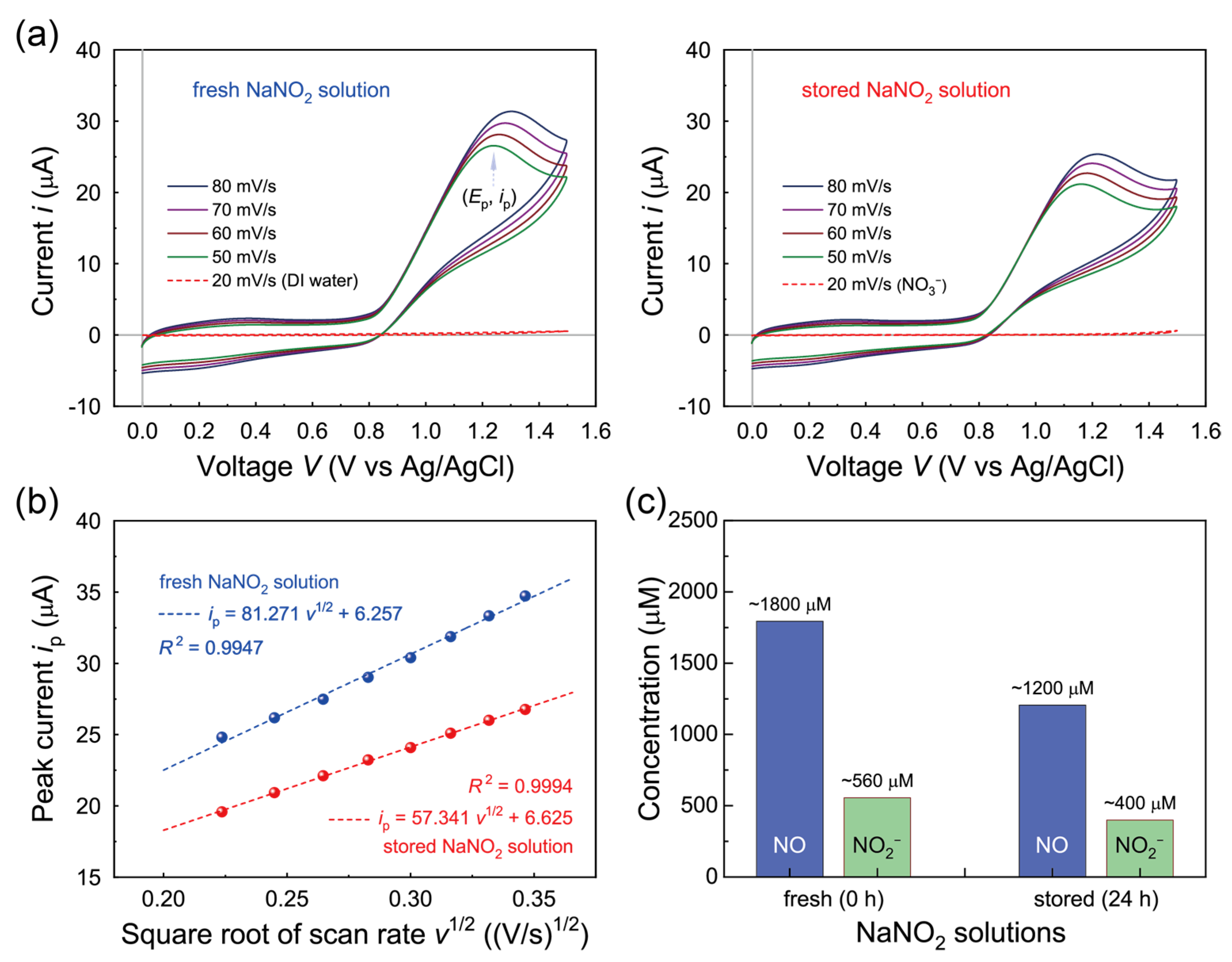
3.1. Characterization of the NaNO2 Aqueous Solution
3.2. Optical 3D Surface Morphologies of SLG Specimen Transferred to Glass Substrates
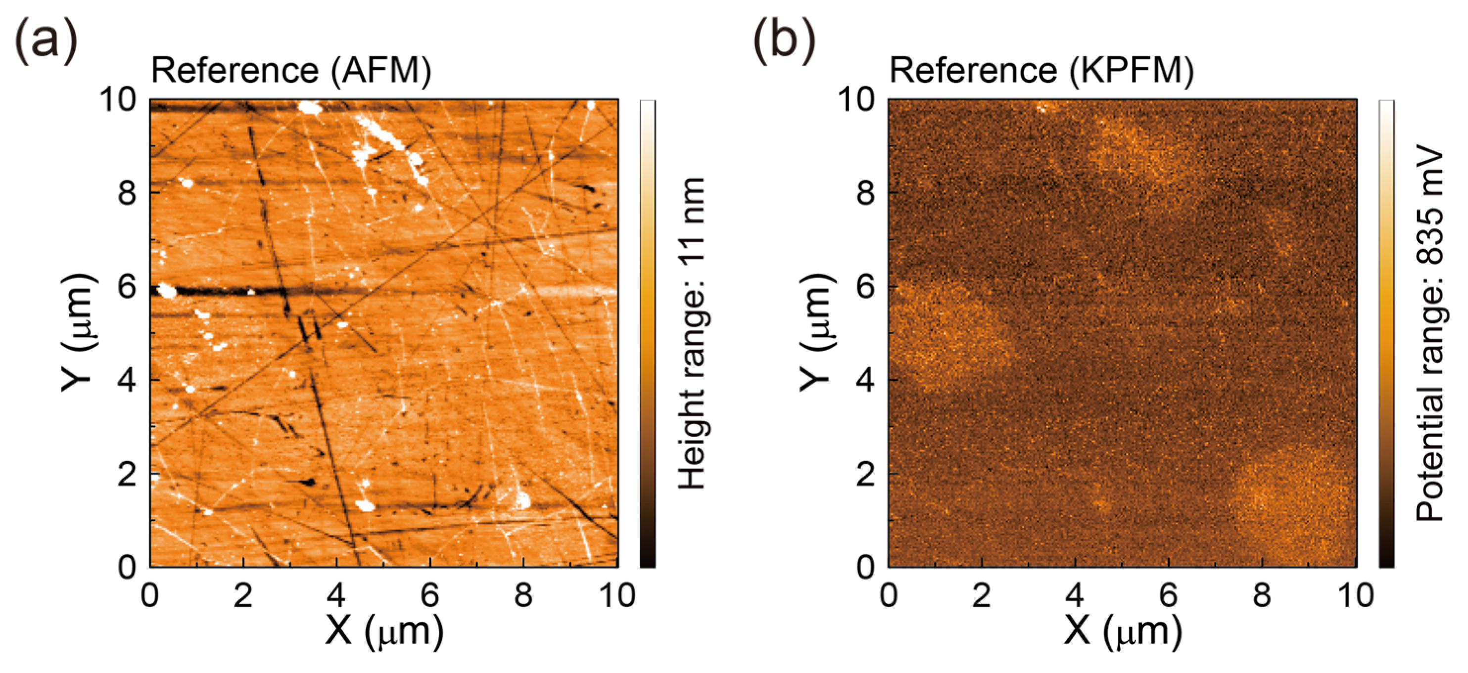
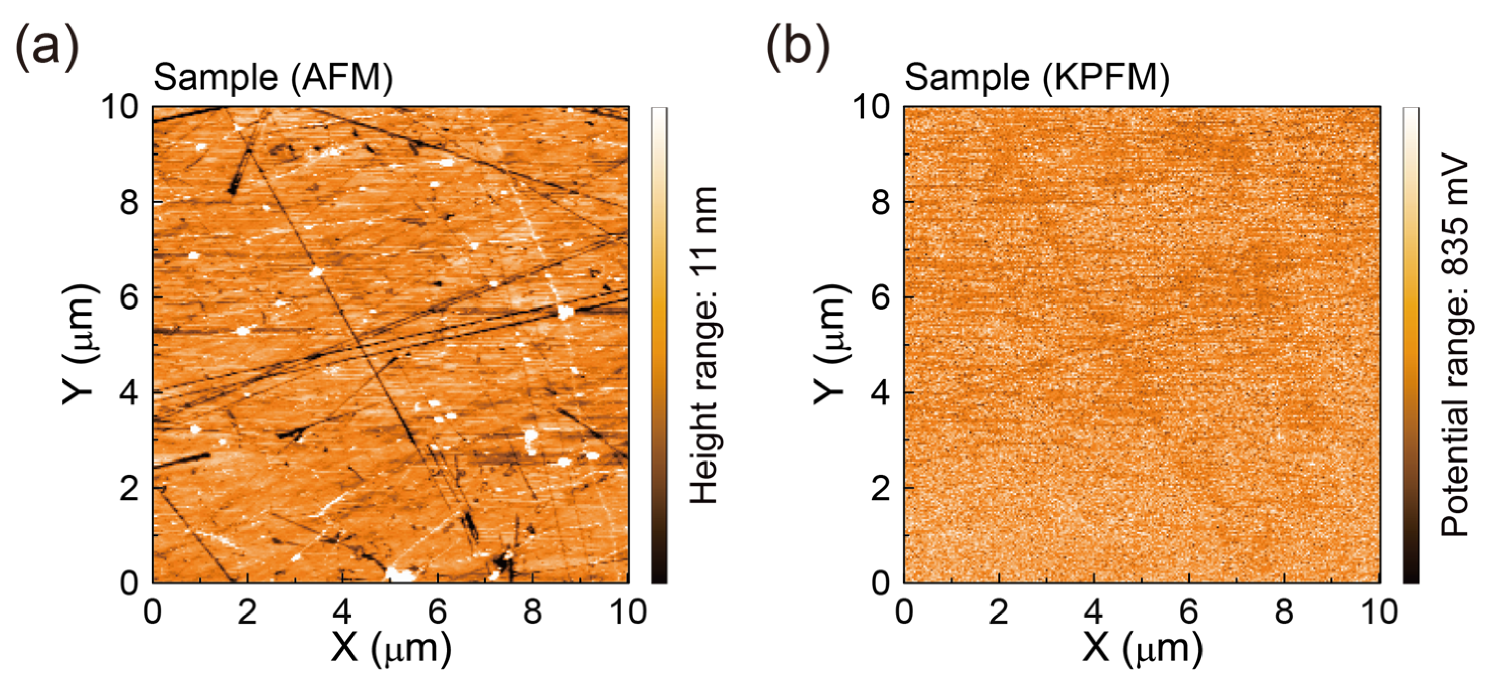
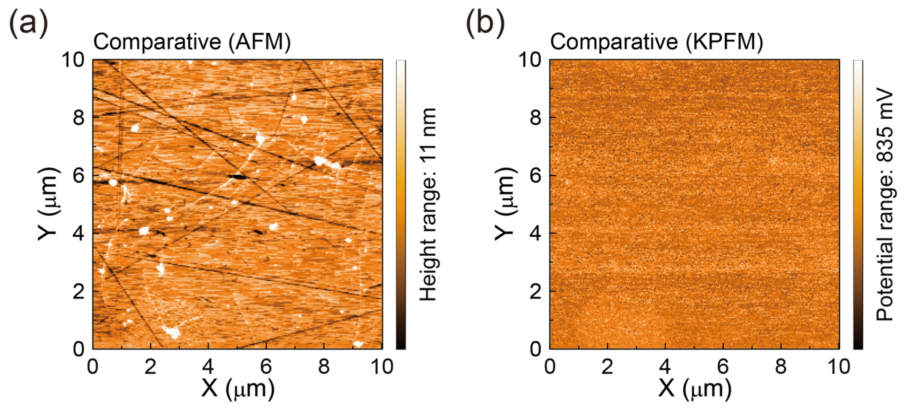
3.3. AFM Surface Morphologies and Surface Potentials of SLG Specimens Transferred to Glass Substrates
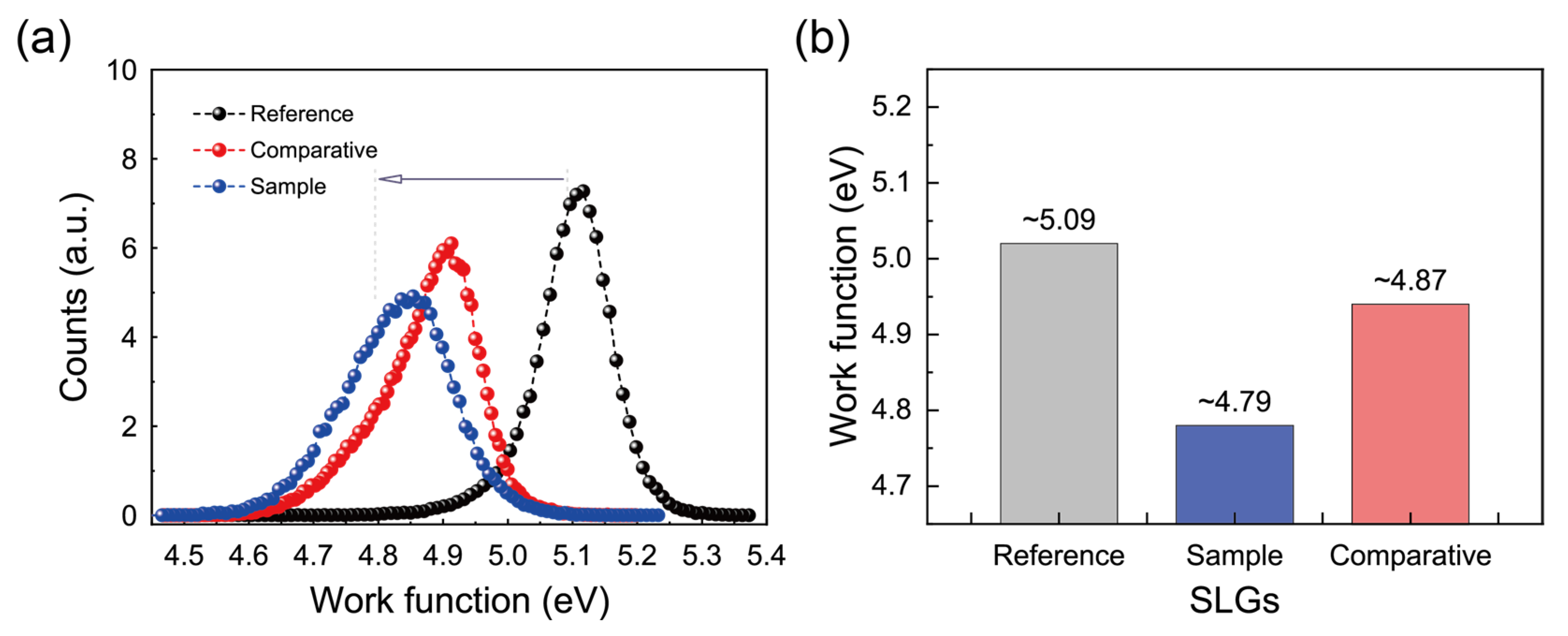
3.4. Work Functions and Compositions of SLG Specimens Transferred to Glass Substrates
3.5. C 1s XPS Spectra of SLG Specimens Transferred to Substrates
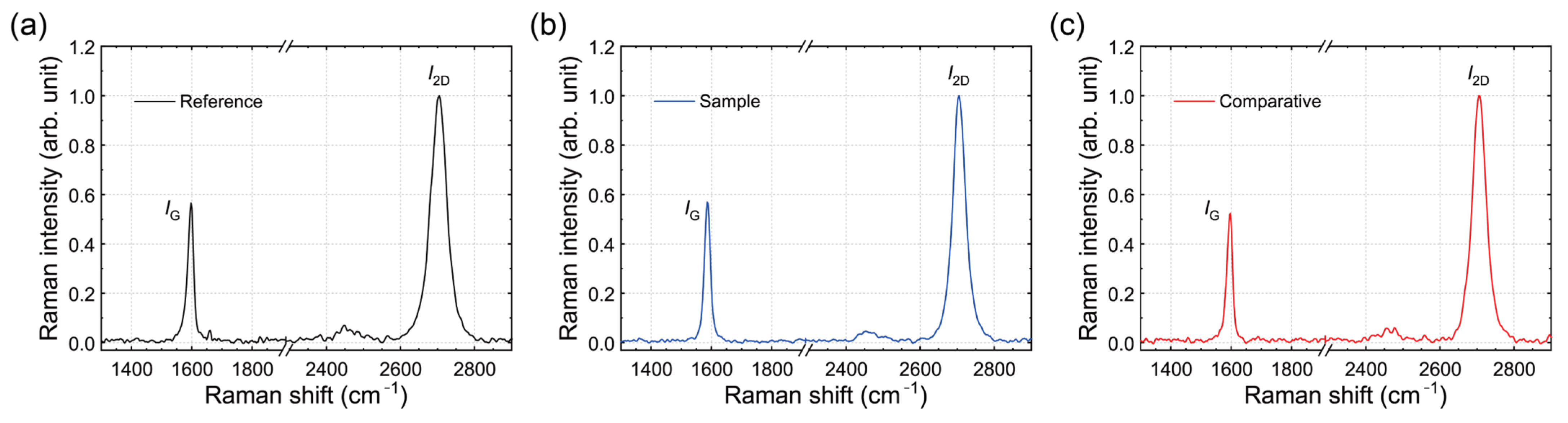
3.6. Raman Spectra of SLG Specimens Transferred to Substrates
4. Conclusions
Author Contributions
Funding
Institutional Review Board Statement
Data Availability Statement
Conflicts of Interest
Appendix A

References
- Berger, C.; Song, Z.; Li, T.; Li, X.; Ogbazghi, A.Y.; Feng, R.; Dai, Z.; Marchenkov, A.N.; Conrad, E.H.; First, P.N.; et al. Ultrathin Epitaxial Graphite: 2D Electron Gas Properties and a Route toward Graphene-Based Nanoelectronics. J. Phys. Chem. B 2004, 108, 19912–19916. [Google Scholar] [CrossRef]
- Castro Neto, A.H.; Guinea, F.; Peres, N.M.R.; Novoselov, K.S.; Geim, A.K. The electronic properties of graphene. Rev. Mod. Phys. 2009, 81, 109–162. [Google Scholar] [CrossRef]
- Geim, A.K.; Novoselov, K.S. The rise of graphene. Nat. Mater. 2007, 6, 183–191. [Google Scholar] [CrossRef] [PubMed]
- Novoselov, K.S.; Geim, A.K.; Morozov, S.V.; Jiang, D.; Katsnelson, M.I.; Grigorieva, I.V.; Dubonos, S.V.; Firsov, A.A. Two-dimensional gas of massless Dirac fermions in graphene. Nature 2005, 438, 197–200. [Google Scholar] [CrossRef]
- Lee, C.; Wei, X.; Kysar, J.W.; Hone, J. Measurement of the Elastic Properties and Intrinsic Strength of Monolayer Graphene. Science 2008, 321, 385–388. [Google Scholar] [CrossRef] [PubMed]
- Rao, C.N.R.; Sood, A.K.; Subrahmanyam, K.S.; Govindaraj, A. Graphene: The New Two-Dimensional Nanomaterial. Angew. Chem. Int. Ed. 2009, 48, 7752–7777. [Google Scholar] [CrossRef] [PubMed]
- Wang, Q.H.; Jin, Z.; Kim, K.K.; Hilmer, A.J.; Paulus, G.L.C.; Shih, C.-J.; Ham, M.-H.; Sanchez-Yamagishi, J.D.; Watanabe, K.; Taniguchi, T.; et al. Understanding and controlling the substrate effect on graphene electron-transfer chemistry via reactivity imprint lithography. Nat. Chem. 2012, 4, 724–732. [Google Scholar] [CrossRef]
- Yang, J.; Hu, P.; Yu, G. Perspective of graphene-based electronic devices: Graphene synthesis and diverse applications. APL Mater. 2019, 7, 020901. [Google Scholar] [CrossRef]
- Howe, L.; Ellepola, K.H.; Jahan, N.; Talbert, B.; Li, J.; Cooney, M.P.; Vinh, N.Q. Characterization and Modeling of Interfacial Photogating Effect in Graphene Field-Effect Transistor Photodetectors on Silicon. ACS Appl. Electron. Mater. 2025, 7, 1305–1313. [Google Scholar] [CrossRef]
- Wang, Z.; Cai, Y.; Jiang, H.; Tian, Z.; Di, Z. Graphene-Based Silicon Photonic Devices for Optical Interconnects. Adv. Funct. Mater. 2024, 34, 2307461. [Google Scholar] [CrossRef]
- Dou, C.; Wu, Z.; Chen, W.; Yan, H.; Li, D.; You, X.-Q.; Chen, Y.-S.; Zhou, C.; Chen, S.; Zhuang, P.; et al. Au-functionalized wrinkle graphene biosensor for ultrasensitive detection of Interleukin-6. Carbon 2024, 216, 118556. [Google Scholar] [CrossRef]
- Lee, J.-Y.; Connor, S.T.; Cui, Y.; Peumans, P. Solution-Processed Metal Nanowire Mesh Transparent Electrodes. Nano Lett. 2008, 8, 689–692. [Google Scholar] [CrossRef] [PubMed]
- Park, B.; Bae, I.-G.; Huh, Y.H. Aligned silver nanowire-based transparent electrodes for engineering polarisation-selective optoelectronics. Sci. Rep. 2016, 6, 19485. [Google Scholar] [CrossRef]
- Ahn, J.; Hwang, H.; Jeong, S.; Moon, J. Metal-Nanowire-Electrode-Based Perovskite Solar Cells: Challenging Issues and New Opportunities. Adv. Energy Mater. 2017, 7, 1602751. [Google Scholar] [CrossRef]
- Ding, Y.; Xiong, S.; Sun, L.; Wang, Y.; Zhou, Y.; Li, Y.; Peng, J.; Fukuda, K.; Someya, T.; Liu, R.; et al. Metal nanowire-based transparent electrode for flexible and stretchable optoelectronic devices. Chem. Soc. Rev. 2024, 53, 7784–7827. [Google Scholar] [CrossRef]
- Wu, Z.; Chen, Z.; Du, X.; Logan, J.M.; Sippel, J.; Nikolou, M.; Kamaras, K.; Reynolds, J.R.; Tanner, D.B.; Hebard, A.F.; et al. Transparent, Conductive Carbon Nanotube Films. Science 2004, 305, 1273–1276. [Google Scholar] [CrossRef] [PubMed]
- Zhu, S.; Ni, J.; Li, Y. Carbon nanotube-based electrodes for flexible supercapacitors. Nano Res. 2020, 13, 1825–1841. [Google Scholar] [CrossRef]
- Khrapach, I.; Withers, F.; Bointon, T.H.; Polyushkin, D.K.; Barnes, W.L.; Russo, S.; Craciun, M.F. Novel Highly Conductive and Transparent Graphene-Based Conductors. Adv. Mater. 2012, 24, 2844–2849. [Google Scholar] [CrossRef]
- Du, J.H.; Jin, H.; Zhang, Z.K.; Zhang, D.D.; Jia, S.; Ma, L.P.; Ren, W.C.; Cheng, H.M.; Burn, P.L. Efficient organic photovoltaic cells on a single layer graphene transparent conductive electrode using MoOx as an interfacial layer. Nanoscale 2017, 9, 251–257. [Google Scholar] [CrossRef]
- Sharif, P.; Alemdar, E.; Ozturk, S.; Caylan, O.; Haciefendioglu, T.; Buke, G.; Aydemir, M.; Danos, A.; Monkman, A.P.; Yildirim, E.; et al. Rational Molecular Design Enables Efficient Blue TADF−OLEDs with Flexible Graphene Substrate. Adv. Funct. Mater. 2022, 32, 2207324. [Google Scholar] [CrossRef]
- Zhang, Y.; Zhang, L.; Zhou, C. Review of Chemical Vapor Deposition of Graphene and Related Applications. Acc. Chem. Res. 2013, 46, 2329–2339. [Google Scholar] [CrossRef] [PubMed]
- Adetayo, A.E.; Ahmed, T.N.; Zakhidov, A.; Beall, G.W. Improvements of Organic Light-Emitting Diodes Using Graphene as an Emerging and Efficient Transparent Conducting Electrode Material. Adv. Optical Mater. 2021, 9, 2002102. [Google Scholar] [CrossRef]
- Li, X.; Cai, W.; An, J.; Kim, S.; Nah, J.; Yang, D.; Piner, R.; Velamakanni, A.; Jung, I.; Tutuc, E.; et al. Large-Area Synthesis of High-Quality and Uniform Graphene Films on Copper Foils. Science 2009, 324, 1312–1314. [Google Scholar] [CrossRef]
- Song, Y.; Zou, W.; Lu, Q.; Lin, L.; Liu, Z. Graphene Transfer: Paving the Road for Applications of Chemical Vapor Deposition Graphene. Small 2021, 17, 2007600. [Google Scholar] [CrossRef]
- Chen, S.; Chen, G.; Zhao, Y.; Bu, S.; Hu, Z.; Mao, B.; Wu, H.; Liao, J.; Li, F.; Zhou, C.; et al. Tunable Adhesion for All-Dry Transfer of 2D Materials Enabled by the Freezing of Transfer Medium. Adv. Mater. 2024, 36, 2308950. [Google Scholar] [CrossRef] [PubMed]
- NaKatani, M.; Fukamachi, S.; Solís-Fernández, P.; Honda, S.; Kawahara, K.; Tsuji, Y.; Sumiya, Y.; Kuroki, M.; Liu, Q. Ready-to-transfer two-dimensional materials using tunable adhesive force tapes. Nat. Electron. 2024, 7, 119–130. [Google Scholar] [CrossRef]
- Xiao, Z.; Wan, Q.; Durkan, C. Cleaning Transferred Graphene for Optimization of Device Performance. Adv. Mater. Interfaces 2019, 6, 1801794. [Google Scholar] [CrossRef]
- Pirkle, A.; Chan, J.; Venugopal, A.; Hinojos, D.; Magnuson, C.W.; McDonnell, S.; Colombo, L.; Vogel, E.M.; Ruoff, R.S.; Wallace, R.M. The effect of chemical residues on the physical and electrical properties of chemical vapor deposited graphene transferred to SiO2. Appl. Phys. Lett. 2011, 99, 122108. [Google Scholar] [CrossRef]
- Chen, J.-H.; Jang, C.; Adam, S.; Fuhrer, M.S.; Williams, E.D.; Ishigami, M. Charged-impurity scattering in graphene. Nat. Phys. 2008, 4, 377–381. [Google Scholar] [CrossRef]
- Schedin, F.; Geim, A.K.; Morozov, S.V.; Hill, E.W.; Blake, P.; Katsnelson, M.I.; Novoselov, K.S. Detection of individual gas molecules adsorbed on graphene. Nat. Mater. 2007, 6, 652–655. [Google Scholar] [CrossRef]
- Ryu, S.; Liu, L.; Berciaud, S.; Yu, Y.-J.; Liu, H.; Kim, P.; Flynn, G.W.; Brus, L.E. Atmospheric Oxygen Binding and Hole Doping in Deformed Graphene on a SiO2 Substrate. Nano Lett. 2010, 10, 4944–4951. [Google Scholar] [CrossRef] [PubMed]
- Song, H.S.; Li, S.L.; Miyazaki, H.; Sato, S.; Hayashi, K.; Yamada, A.; Yokoyama, N.; Tsukagoshi, K. Origin of the relatively low transport mobility of graphene grown through chemical vapor deposition. Sci. Rep. 2012, 2, 337. [Google Scholar] [CrossRef] [PubMed]
- Yu Wang, Y.; Burke, P.J. A large-area and contamination-free graphene transistor for liquid-gated sensing applications. Appl. Phys. Lett. 2013, 103, 052103. [Google Scholar] [CrossRef]
- Park, I.-J.; Kim, T.I.; Choi, S.-Y. Charge Transfer Dynamics of Doped Graphene Electrodes for Organic Light-Emitting Diodes. ACS Appl. Mater. Interfaces 2022, 14, 43907–43916. [Google Scholar] [CrossRef] [PubMed]
- Ambrosi, A.; Pumera, M. The CVD graphene transfer procedure introduces metallic impurities which alter the graphene electrochemical properties. Nanoscale 2014, 6, 472–476. [Google Scholar] [CrossRef]
- Zhuang, B.; Li, S.; Li, S.; Yin, J. Ways to eliminate PMMA residues on graphene—Superclean graphene. Carbon 2021, 173, 609–636. [Google Scholar] [CrossRef]
- Lin, Y.-C.; Lu, C.-C.; Yeh, C.-H.; Jin, C.; Suenaga, K.; Chiu, P.-W. Graphene Annealing: How Clean Can It Be? Nano Lett. 2012, 12, 414–419. [Google Scholar] [CrossRef]
- Gong, C.; Floresca, H.C.; Hinojos, D.; McDonnell, S.; Qin, X.; Hao, Y.; Jandhyala, S.; Mordi, G.; Kim, J.; Colombo, L.; et al. Rapid Selective Etching of PMMA Residues from Transferred Graphene by Carbon Dioxide. J. Phys. Chem. C 2013, 117, 23000–23008. [Google Scholar] [CrossRef]
- Gao, Y.; Chen, J.; Chen, G.; Fan, C.; Liu, X. Recent Progress in the Transfer of Graphene Films and Nanostructures. Small Methods 2021, 5, 2100771. [Google Scholar] [CrossRef]
- Choi, W.J.; Chung, Y.J.; Park, S.; Yang, C.-S.; Lee, Y.K.; An, K.-S.; Lee, Y.-S.; Lee, J.-O. A Simple Method for Cleaning Graphene Surfaces with an Electrostatic Force. Adv. Mater. 2014, 26, 637–644. [Google Scholar] [CrossRef]
- Xia, Y.; Sun, Y.; Li, H.; Chen, S.; Zhu, T.; Wang, G.; Man, B.; Pan, J.; Yang, C. Plasma treated graphene FET sensor for the DNA hybridization detection. Talanta 2021, 223, 121766. [Google Scholar] [CrossRef] [PubMed]
- Park, B.; Huh, J.N.; Lee, W.S.; Bae, I.-G. Simple and rapid cleaning of graphenes with a ‘bubble-free’ electrochemical treatment. J. Mater. Chem. C 2018, 6, 2234–2244. [Google Scholar] [CrossRef]
- Cherian, C.T.; Giustiniano, F.; Martin-Fernandez, I.; Andersen, H.; Balakrishnan, J.; Özyilmaz, B. ‘Bubble-Free’ Electrochemical Delamination of CVD Graphene Films. Small 2015, 11, 189–194. [Google Scholar] [CrossRef]
- Mbayachi, V.B.; Ndayiragije, E.; Sammani, T.; Taj, S.; Mbuta, E.R.; Khan, A.U. Graphene synthesis, characterization and its applications: A review. Results Chem. 2021, 3, 100163. [Google Scholar] [CrossRef]
- Suk, J.W.; Kitt, A.; Magnuson, C.W.; Hao, Y.; Ahmed, S.; An, J.; Swan, A.K.; Goldberg, B.B.; Ruoff, R.S. Transfer of CVD-Grown Monolayer Graphene onto Arbitrary Substrates. ACS Nano 2011, 5, 6916–6924. [Google Scholar] [CrossRef]
- Abdelaal, A.F.; Laoui, T.; Ibrahim, A.; Asafa, T.B.; Salhi, B.; Bhuiyan, S.I. Polymethylmethacrylate (PMMA) deposition and removal optimization in CVD-grown graphene transfer: A Taguchi technique study. Diam. Relat. Mater. 2024, 149, 111660. [Google Scholar] [CrossRef]
- Noyes, W.A. Preparation of Nitric Oxide from Sodium Nitrite. J. Am. Chem. Soc. 1925, 47, 2170. [Google Scholar] [CrossRef]
- Klyamer, D.; Shutilov, R.; Basova, T. Recent Advances in Phthalocyanine and Porphyrin-Based Materials as Active Layers for Nitric Oxide Chemical Sensors. Sensors 2022, 22, 895. [Google Scholar] [CrossRef]
- Faulkner, L.R.; Bard, A.J. Electrochemical Methods: Fundamentals and Applications; John Wiley & Sons: Hoboken, NJ, USA, 2001. [Google Scholar]
- Zhou, Z.; Todd, B.D.; Travis, K.P.; Sadus, R.J. A molecular dynamics study of nitric oxide in water: Diffusion and structure. J. Chem. Phys. 2005, 123, 054505. [Google Scholar] [CrossRef]
- Yu, Y.-J.; Zhao, Y.; Ryu, S.; Brus, L.E.; Kim, K.S.; Kim, P. Tuning the Graphene Work Function by Electric Field Effect. Nano Lett. 2009, 9, 3430–3434. [Google Scholar] [CrossRef]
- Zhao, C.; Shan, L.; Sun, R.; Wang, X.; Ding, F. Wrinkle formation in synthesized graphene and 2D materials. Mater. Today 2024, 81, 104–117. [Google Scholar] [CrossRef]
- Panchal, V.; Pearce, R.; Yakimova, R.; Tzalenchuk, A.; Kazakova, O. Standardization of surface potential measurements of graphene domains. Sci. Rep. 2013, 3, 2597. [Google Scholar] [CrossRef] [PubMed]
- Liu, W.; Kang, J.; Banerjee, K. Characterization of FeCl3 Intercalation Doped CVD Few-Layer Graphene. IEEE Electron Device Lett. 2016, 37, 1246–1249. [Google Scholar] [CrossRef]
- Huang, S.-D.; Chu, E.-D.; Wang, Y.-H.; Liou, J.-W.; Wang, R.-S.; Woon, W.-Y.; Chiu, H.-C. Variations in the Effective Work Function of Graphene in a Sliding Electrical Contact Interface under Ambient Conditions. ACS Appl. Mater. Interfaces 2022, 14, 27328–27338. [Google Scholar] [CrossRef] [PubMed]
- Legesse, M.; Rashkeev, S.N.; Al-Dirini, F.; Alharbi, F.H. Tunable high workfunction contacts: Doped graphene. Appl. Surf. Sci. 2020, 509, 144893. [Google Scholar] [CrossRef]
- Gengenbach, T.R.; Major, G.H.; Linford, M.R.; Easton, C.D. Practical guides for x-ray photoelectron spectroscopy (XPS): Interpreting the carbon 1s spectrum. J. Vac. Sci. Technol. A 2021, 39, 013204. [Google Scholar] [CrossRef]
- Major, G.H.; Fernandez, V.; Fairly, N.; Smith, E.F.; Linford, M.R. Guide to XPS Data Analysis: Applying Appropriate Constraints to Synthetic Peaks in XPS Peak Fitting. J. Vac. Sci. Technol. A 2022, 40, 063201. [Google Scholar] [CrossRef]
- Vinogradov, N.A.; Simonov, K.A.; Generalov, A.V.; Vinogradov, A.S.; Vyalikh, D.V.; Laubschat, C.; Mårtensson, N.; Preobrajenski, A.B. Controllable p-doping of graphene on Ir(111) by chlorination with FeCl3. J. Phys. Condens. Matter 2012, 24, 314202. [Google Scholar] [CrossRef]
- Xing, Z.; Jiang, X.; Cracknell, R.F. Investigation of the chemical mechanism of pollutant formation in co-firing of ammonia and biomass lignin. Int. J. Hydrog. Energy 2024, 77, 126–137. [Google Scholar] [CrossRef]
- Zhou, H.; Qiu, C.; Yu, F.; Yang, H.; Chen, M.; Hu, L.; Guo, Y.; Sun, L. Raman scattering of monolayer graphene: The temperature and oxygen doping effects. J. Phys. D Appl. Phys. 2011, 44, 185404. [Google Scholar] [CrossRef]
- Erkan, S.; Yagmyrov, A.; Altuntepe, A.; Zan, R.; Olgar, M.A. Integration of single layer graphene into CZTS thin film solar cells. J. Alloys Compd. 2022, 920, 166041. [Google Scholar] [CrossRef]
- Ryu, S.; Maultzsch, J.; Han, M.Y.; Kim, P.; Brus, L.E. Raman Spectroscopy of Lithographically Patterned Graphene Nanoribbons. ACS Nano 2011, 5, 4123–4130. [Google Scholar] [CrossRef] [PubMed]
- Kim, S.J.; Park, S.J.; Kim, H.Y.; Jang, G.S.; Park, D.J.; Park, J.-Y.; Lee, S.; Ahn, Y.H. Characterization of chemical doping of graphene by in-Situ Raman spectroscopy. Appl. Phys Lett. 2016, 108, 203111. [Google Scholar] [CrossRef]
- Fukamachi, S.; Solís-Fernández, P.; Kawahara, K.; Tanaka, D.; Otake, T.; Lin, Y.-C.; Suenaga, K.; Ago, H. Large-area synthesis and transfer of multilayer hexagonal boron nitride for enhanced graphene device arrays. Nat. Electron. 2023, 6, 126–136. [Google Scholar] [CrossRef]
- Mallik, S.K.; Padhan, R.; Roy, S.; Sahu, M.C.; Sahoo, S.; Sahoo, S. Direct Transfer of Monolayer MoS2 Device Arrays for Potential Applications in Flexible Electronics. ACS Appl. Nano Mater. 2024, 7, 4796–4804. [Google Scholar] [CrossRef]


| SLG Specimen | Rinsing with | Sheet Resistance (Ω/□) | Conductivity σ (×106 S/m) | Mobility μ (×104 cm2/Vs) | Work Function (eV) |
|---|---|---|---|---|---|
| Reference | DI water | 653 ± 106 | 4.55 ± 0.84 | 2.80 ± 0.52 | 5.09 ± 0.05 |
| Sample | Fresh NaNO2 solution | 883 ± 49 | 3.29 ± 0.18 | 2.03 ± 0.11 | 4.79 ± 0.08 |
| Comparative | Stored NaNO2 solution (24 h) | 851 ± 102 | 3.45 ± 0.46 | 2.12 ± 0.28 | 4.87 ± 0.07 |
Disclaimer/Publisher’s Note: The statements, opinions and data contained in all publications are solely those of the individual author(s) and contributor(s) and not of MDPI and/or the editor(s). MDPI and/or the editor(s) disclaim responsibility for any injury to people or property resulting from any ideas, methods, instructions or products referred to in the content. |
© 2025 by the authors. Licensee MDPI, Basel, Switzerland. This article is an open access article distributed under the terms and conditions of the Creative Commons Attribution (CC BY) license (https://creativecommons.org/licenses/by/4.0/).
Share and Cite
Lee, K.; Kil, J.; Park, J.; Yang, S.; Park, B. Rapid and Efficient Polymer/Contaminant Removal from Single-Layer Graphene via Aqueous Sodium Nitrite Rinsing for Enhanced Electronic Applications. Polymers 2025, 17, 689. https://doi.org/10.3390/polym17050689
Lee K, Kil J, Park J, Yang S, Park B. Rapid and Efficient Polymer/Contaminant Removal from Single-Layer Graphene via Aqueous Sodium Nitrite Rinsing for Enhanced Electronic Applications. Polymers. 2025; 17(5):689. https://doi.org/10.3390/polym17050689
Chicago/Turabian StyleLee, Kimin, Juneyoung Kil, JaeWoo Park, Sui Yang, and Byoungchoo Park. 2025. "Rapid and Efficient Polymer/Contaminant Removal from Single-Layer Graphene via Aqueous Sodium Nitrite Rinsing for Enhanced Electronic Applications" Polymers 17, no. 5: 689. https://doi.org/10.3390/polym17050689
APA StyleLee, K., Kil, J., Park, J., Yang, S., & Park, B. (2025). Rapid and Efficient Polymer/Contaminant Removal from Single-Layer Graphene via Aqueous Sodium Nitrite Rinsing for Enhanced Electronic Applications. Polymers, 17(5), 689. https://doi.org/10.3390/polym17050689