Influence of Manufacturing Parameters and Post Processing on the Electrical Conductivity of Extrusion-Based 3D Printed Nanocomposite Parts


Abstract
:
1. Introduction
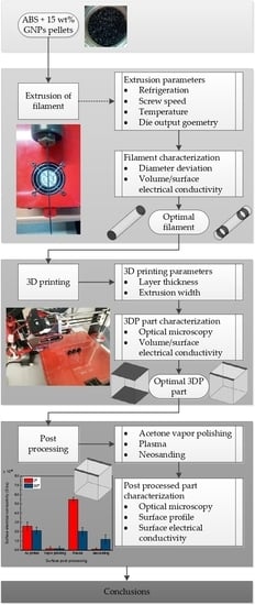
2. Materials and Methods
2.1. Materials
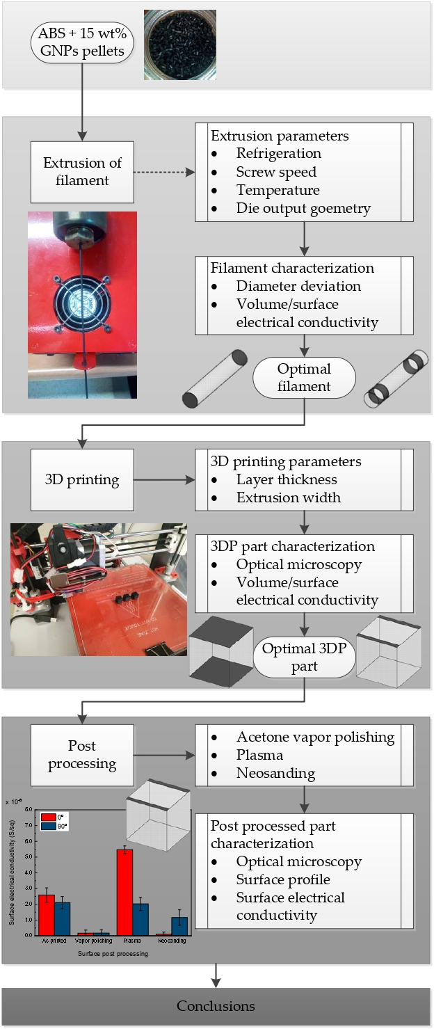
2.2. Manufacturing
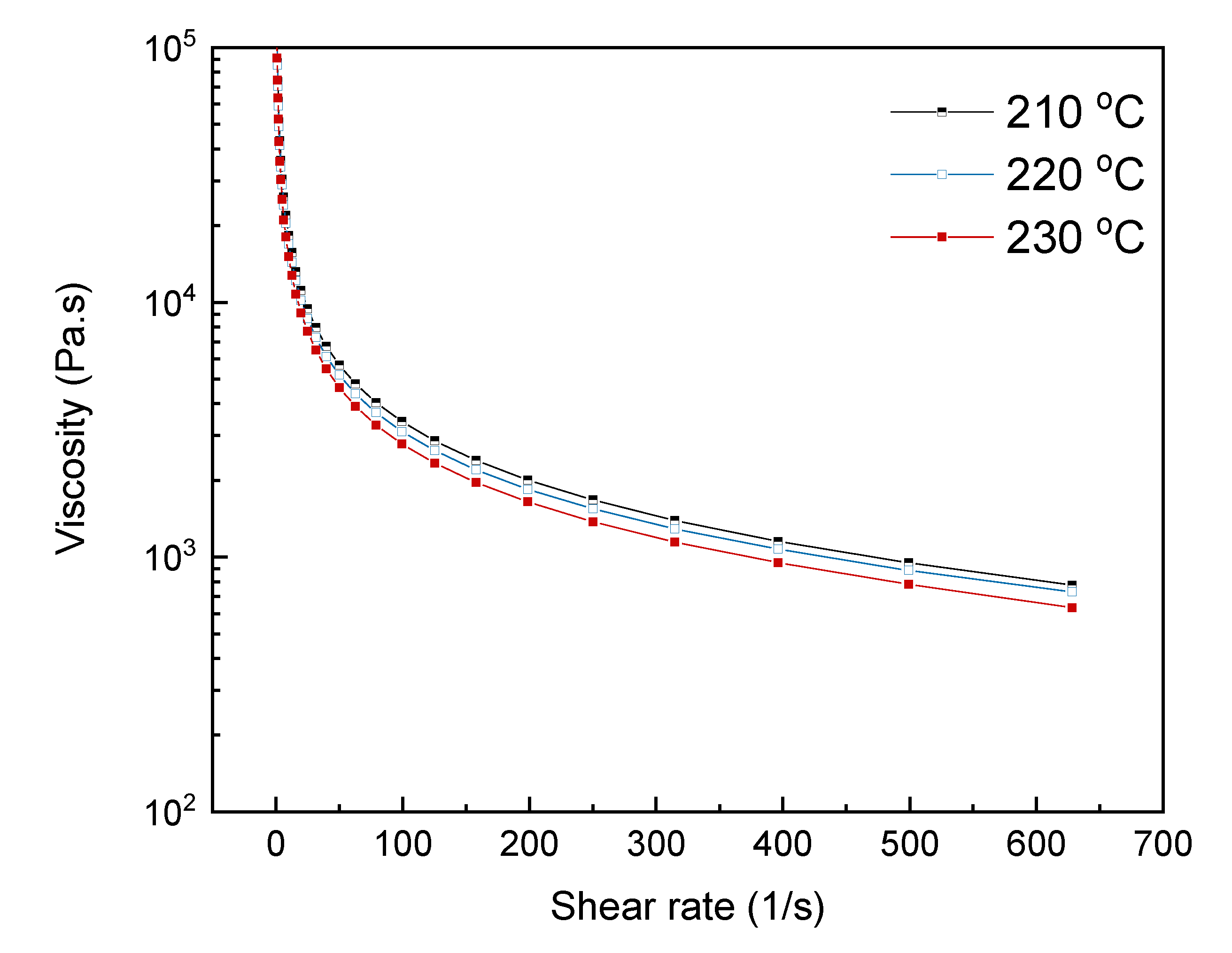
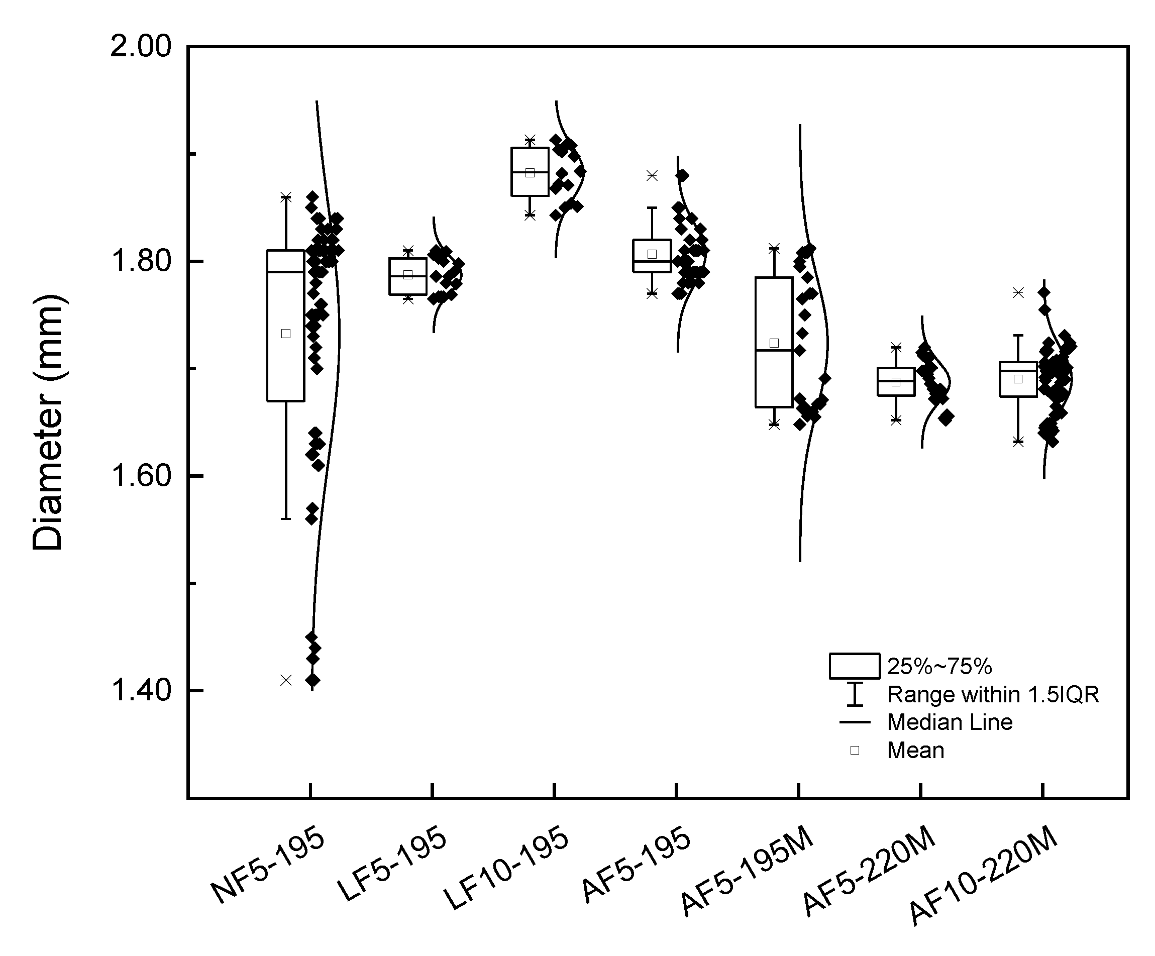
2.2.1. Filament
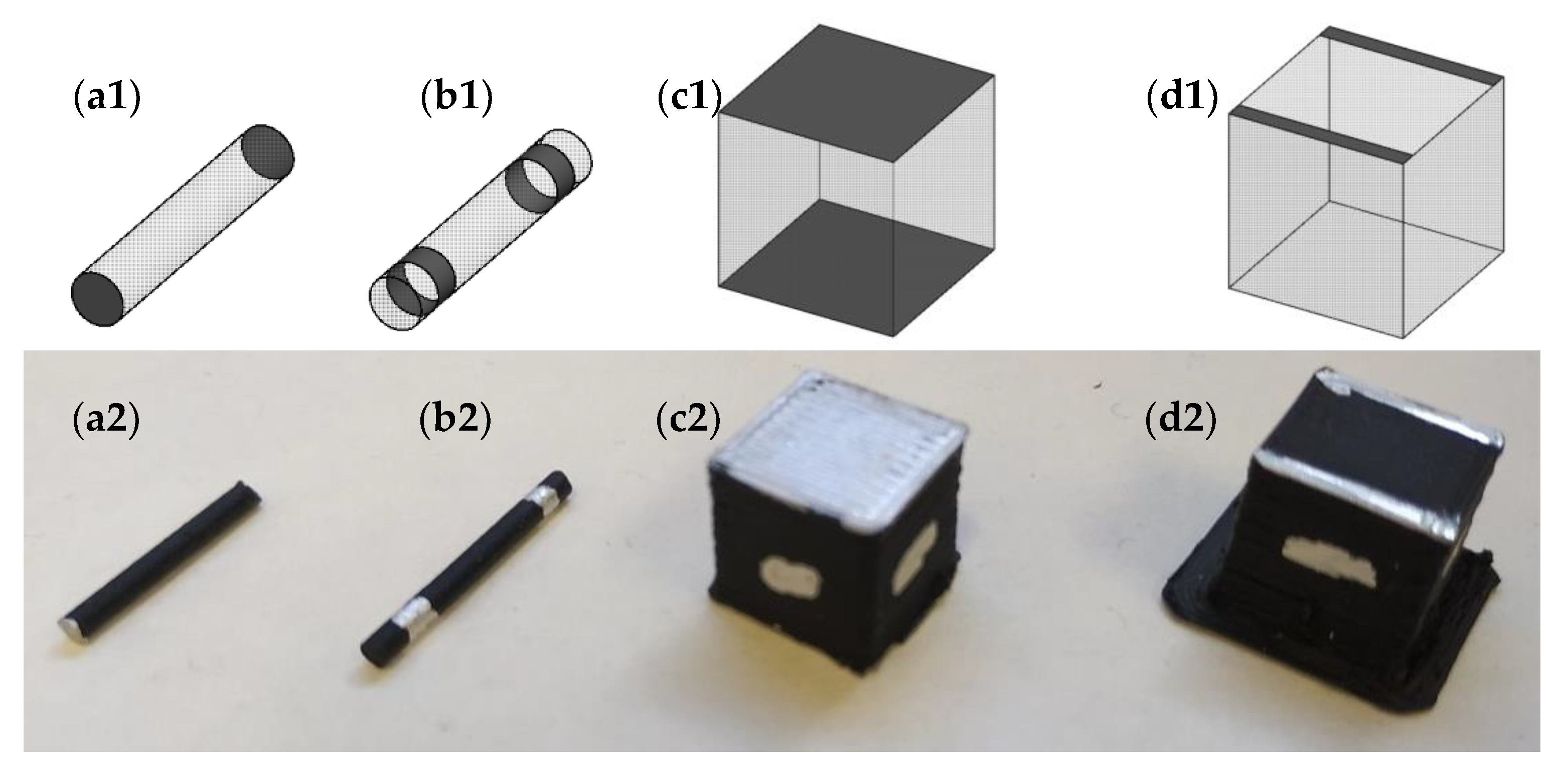
2.2.2. 3D printed Parts
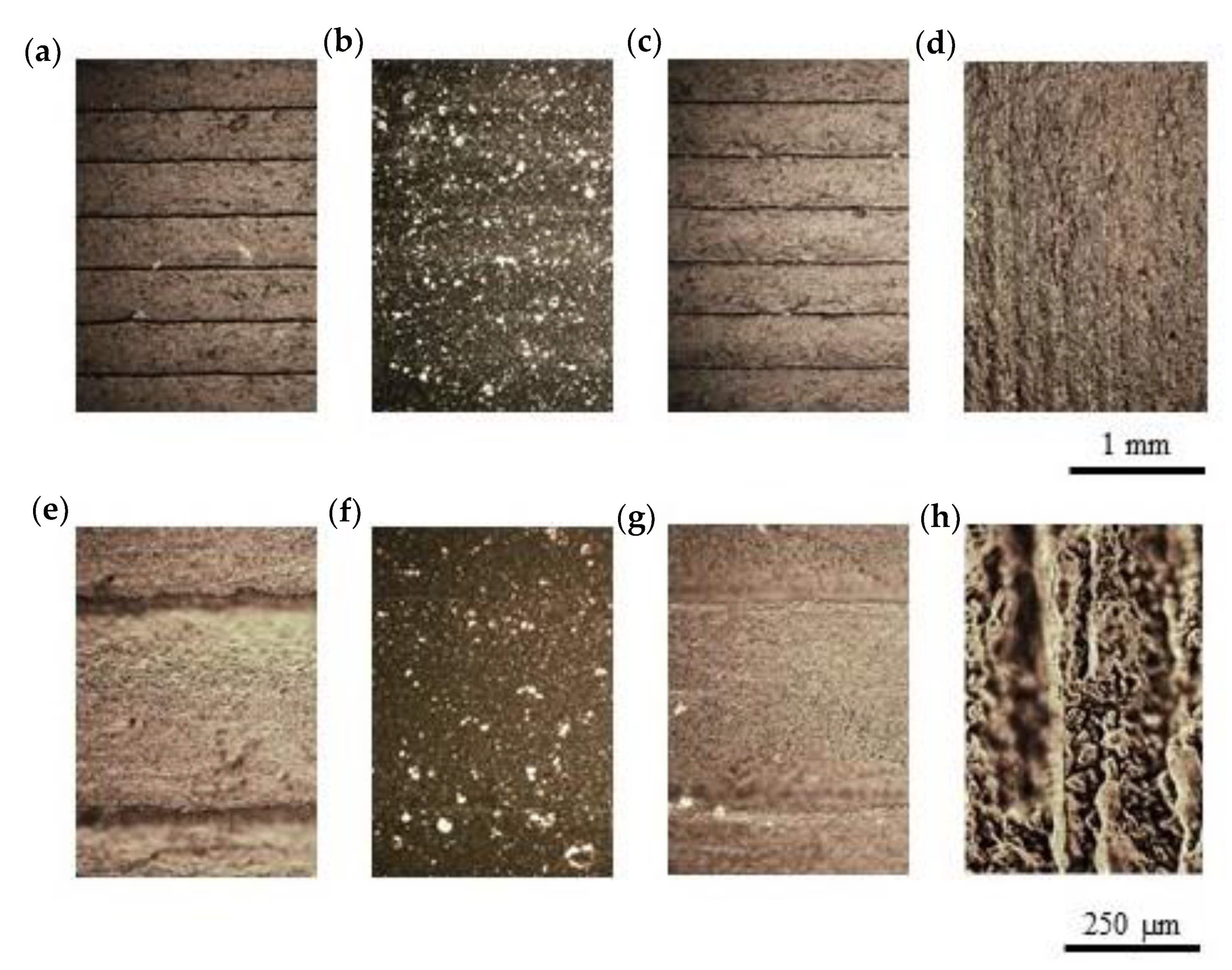
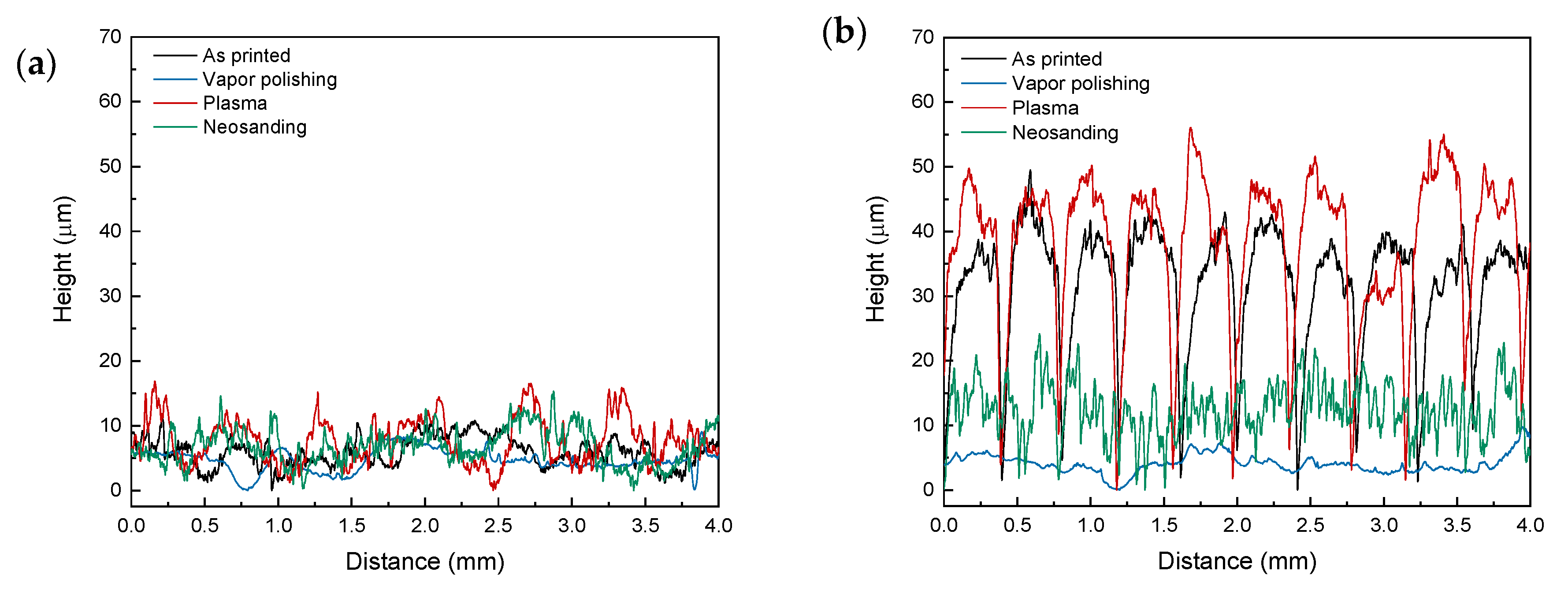
2.2.3. Post Processing
- Acetone post processing. Vapor polishing of 3D-printed parts was carried out under acetone vapor generated at 57 °C for 1 min in a closed content. After surface post processing, samples were dried at 37 °C.
- Plasma post processing. Plasma surface post-processing was conducted in a Zepto plasma unit (Electronic Diener, Plasma Surface Technology). The plasma was generated in O2 atmosphere with a pressure of 1.8 mbar and a power of 70 W [24]. Surfaces of 3D-printed parts were exposed to the oxygen plasma for 3 min.
- Neosanding. Neosanding is a novel in-situ surface post processing that was applied with a 90° path to the direction of the deposited filament of the last layer. The nozzle tip temperature was maintained and the height of the path was reduced 0.05 mm compared with the height of the last printed layer (0.05 mm penetration). On the other hand, the extrusion width was reduced to 0.05 mm. This low value was used as a strategy to avoid the filament extrusion and achieve the neosanding post processing, since the slicer software (Simplify3D) does not include this option. The effect of this process on the electrical conductivity was assessed.
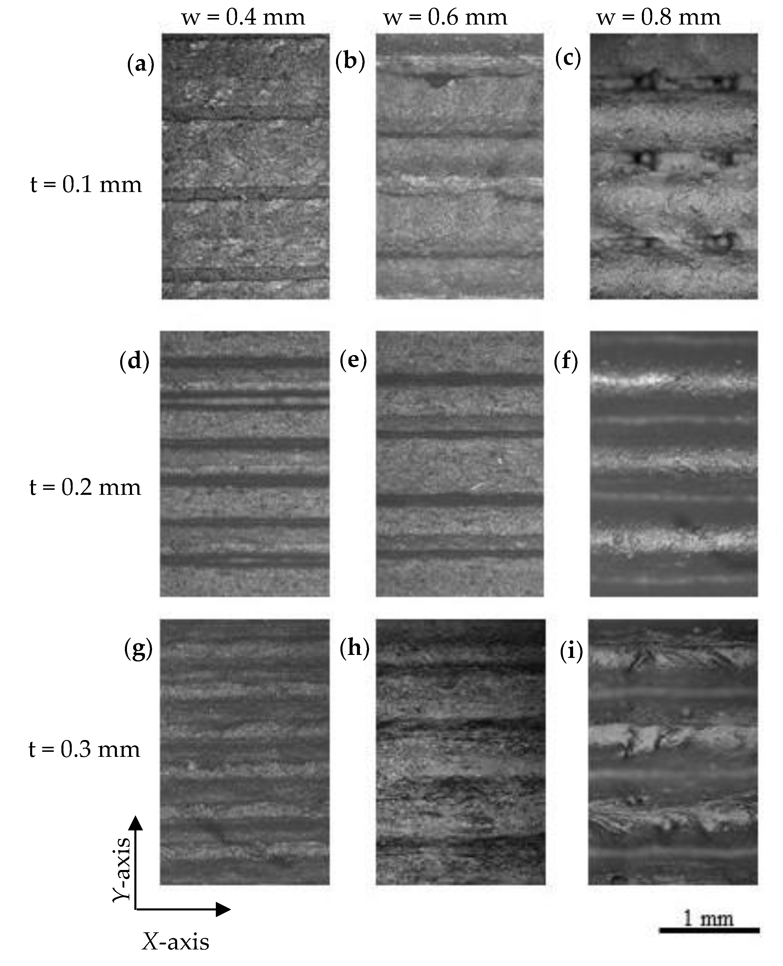
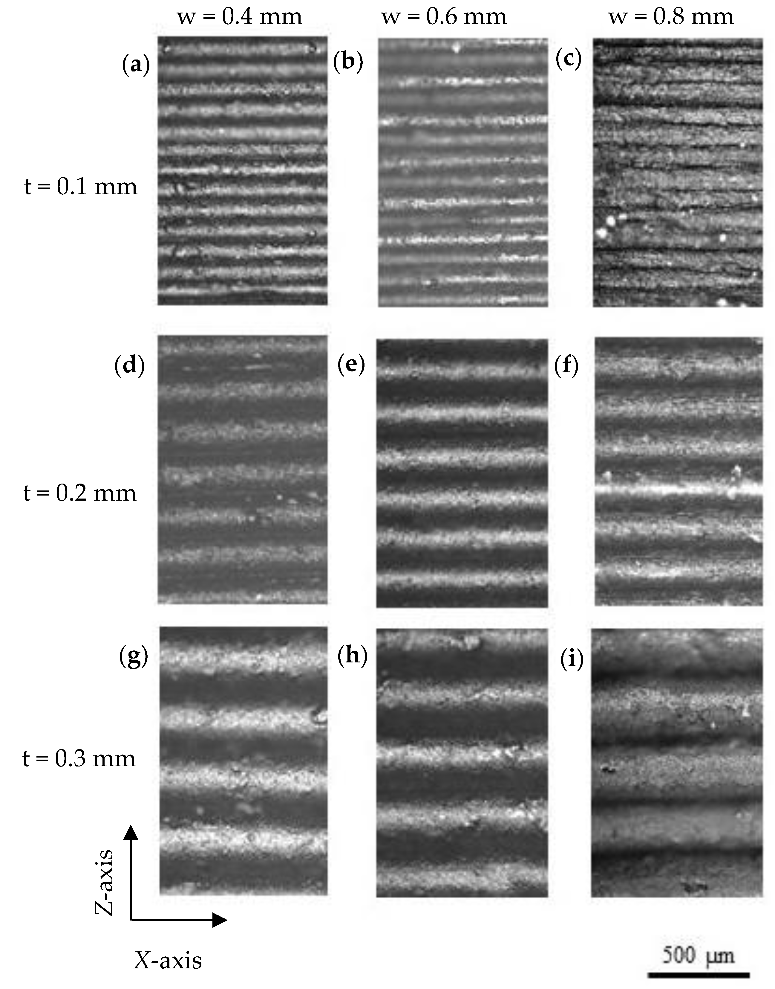
2.3. Morphological and Microstructural Characterization
2.4. Measurement of Volume and Surface Electrical Conductivity
2.4.1. Volume Electrical Conductivity
2.4.2. Surface Electrical Conductivity
3. Results
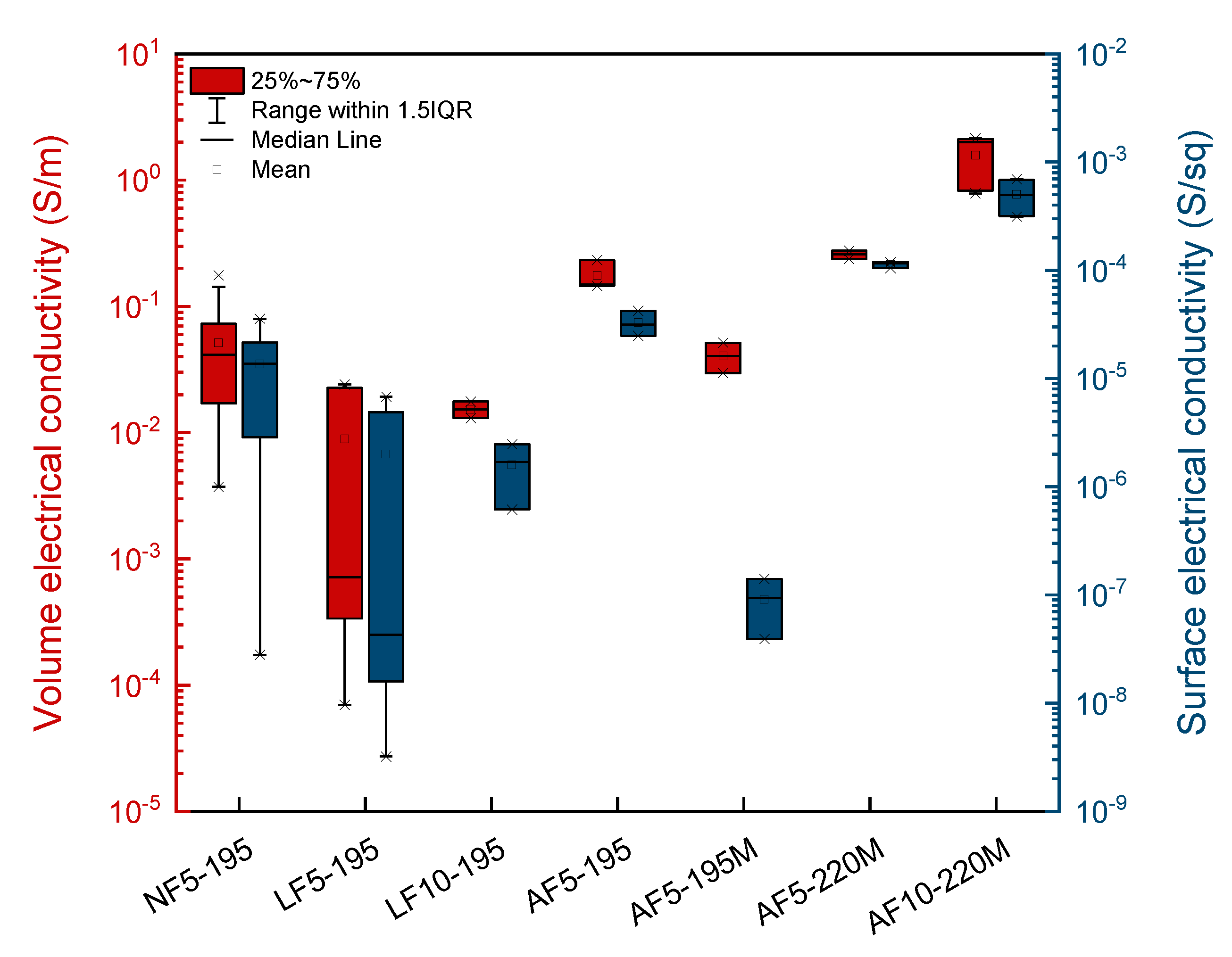
3.1. Measurement of Volume and Surface Electrical Conductivity
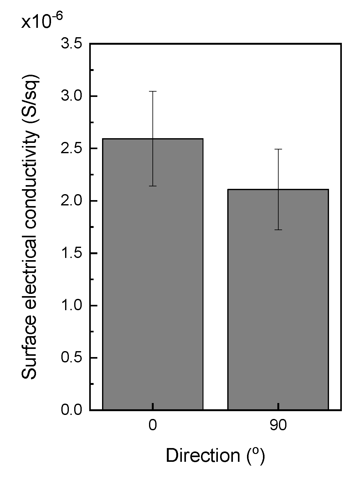
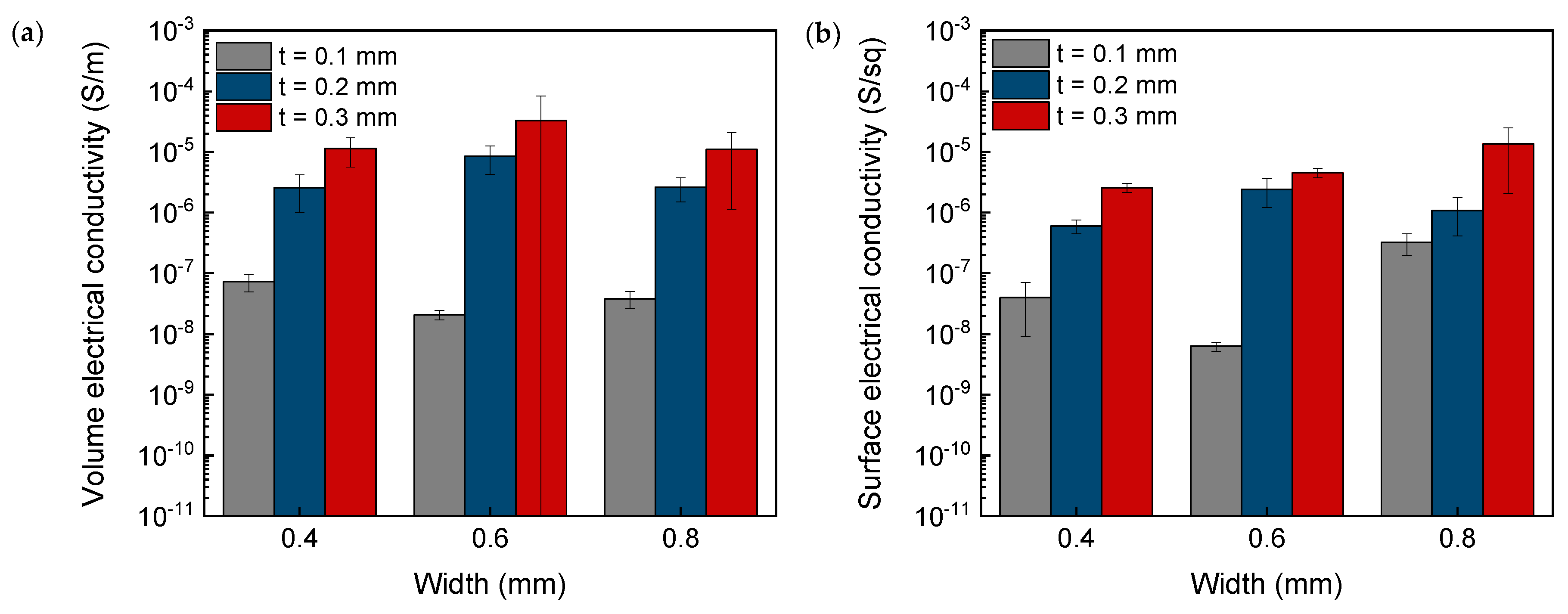
3.2. Influence of 3D Printing Operational Parameters on the Electrical Conductivity of Printed Parts
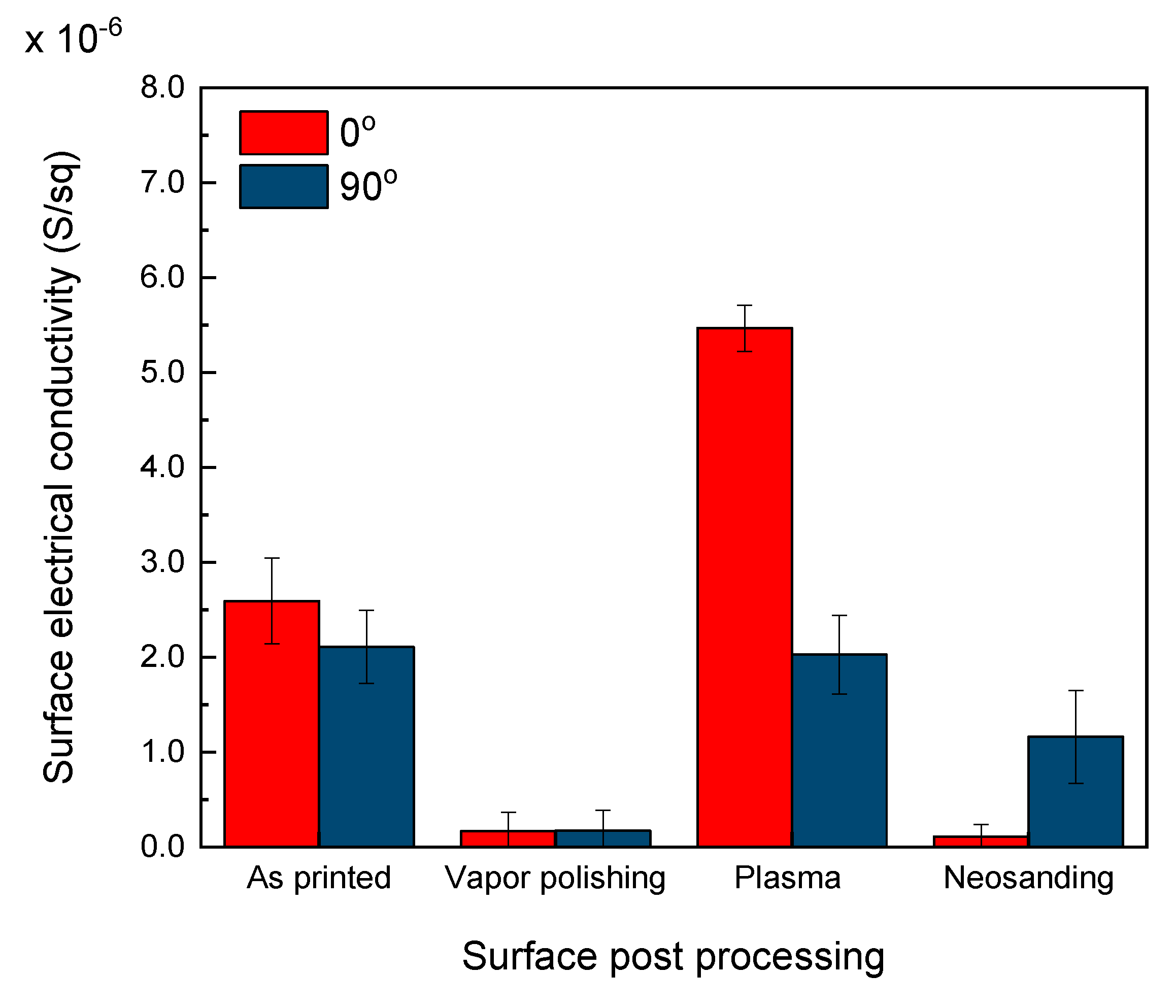
3.3. Influence of Surface Post Processing on the Electrical Conductivity of Printed Parts
4. Conclusions
Author Contributions
Funding
Conflicts of Interest
References
- Sengupta, R.; Bhattacharya, M.; Bandyopadhyay, S.; Bhowmick, A.K. A review on the mechanical and electrical properties of graphite and modified graphite reinforced polymer composites. Prog. Polym. Sci. 2011, 36, 638–670. [Google Scholar] [CrossRef]
- Ghaleb, Z.; Mariatti, M.; Ariff, Z.M. Properties of graphene nanopowder and multi-walled carbon nanotube-filled epoxy thin-film nanocomposites for electronic applications: The effect of sonication time and filler loading. Compos. Part A Appl. Sci. Manuf. 2014, 58, 77–83. [Google Scholar] [CrossRef]
- Qin, W.; Vautard, F.; Drzal, L.T.; Yu, J. Mechanical and electrical properties of carbon fiber composites with incorporation of graphene nanoplatelets at the fiber–matrix interphase. Compos. Part B Eng. 2015, 69, 335–341. [Google Scholar] [CrossRef]
- Xu, H.G.; Qu, M.C.; Pan, Y.M.; Schubert, D.W. Conductivity of Poly(methyl methacrylate)/Polystyrene/Carbon Black and Poly(ethyl methacrylate)/Polystyrene/Carbon Black Ternary Composite Films. Chin. J. Polym. Sci. 2020, 38, 288–297. [Google Scholar] [CrossRef]
- Liu, X.; Li, C.; Pan, Y.; Schubert, D.W.; Liu, C. Shear-induced rheological and electrical properties of molten poly(methyl methacrylate)/carbon black nanocomposites. Compos. Part B Eng. 2019, 164, 37–44. [Google Scholar] [CrossRef]
- Qu, M.; Nilsson, F.; Qin, Y.; Yang, G.; Pan, Y.; Liu, X.; Hernandez Rodriguez, G.; Chen, J.; Zhang, C.; Schubert, D.W. Electrical conductivity and mechanical properties of melt-spun ternary composites comprising PMMA, carbon fibers and carbon black. Compos. Sci. Technol. 2017, 150, 24–31. [Google Scholar] [CrossRef]
- Qin, Y.; Qu, M.; Pan, Y.; Zhang, C.; Schubert, D.W. Fabrication, characterization and modelling of triple hierarchic PET/CB/TPU composite fibres for strain sensing. Compos. Part A Appl. Sci. Manuf. 2020, 129, 105724. [Google Scholar] [CrossRef]
- Li, W.; Dichiara, A.; Bai, J. Carbon nanotube–graphene nanoplatelet hybrids as high-performance multifunctional reinforcements in epoxy composites. Compos. Sci. Technol. 2013, 74, 221–227. [Google Scholar] [CrossRef]
- Kanoun, O.; Müller, C.; Benchirouf, A.; Sanli, A.; Dinh, T.; Al-Hamry, A.; Bu, L.; Gerlach, C.; Bouhamed, A. Flexible Carbon Nanotube Films for High Performance Strain Sensors. Sensors 2014, 14, 10042–10071. [Google Scholar] [CrossRef] [Green Version]
- Chandrasekaran, S.; Seidel, C.; Schulte, K. Preparation and characterization of graphite nano-platelet (GNP)/epoxy nano-composite: Mechanical, electrical and thermal properties. Eur. Polym. J. 2013, 49, 3878–3888. [Google Scholar] [CrossRef]
- Ma, J.; Meng, Q.; Zaman, I.; Zhu, S.; Michelmore, A.; Kawashima, N.; Wang, C.H.; Kuan, H.C. Development of polymer composites using modified, high-structural integrity graphene platelets. Compos. Sci. Technol. 2014, 91, 82–90. [Google Scholar] [CrossRef]
- Singh, V.; Joung, D.; Zhai, L.; Das, S.; Khondaker, S.I.; Seal, S. Graphene based materials: Past, present and future. Prog. Mater. Sci. 2011, 56, 1178–1271. [Google Scholar] [CrossRef]
- Li, J.; Kim, J.K. Percolation threshold of conducting polymer composites containing 3D randomly distributed graphite nanoplatelets. Compos. Sci. Technol. 2007, 67, 2114–2120. [Google Scholar] [CrossRef] [Green Version]
- Monzel, W.J.; Hoff, B.W.; Maestas, S.S.; French, D.M.; Hayden, S.C. Dielectric breakdown of additively manufactured polymeric materials. IEEE Trans. Dielectr. Electr. Insul. 2015, 22, 3543–3549. [Google Scholar] [CrossRef]
- Conner, B.P.; Manogharan, G.P.; Martof, A.N.; Rodomsky, L.M.; Rodomsky, C.M.; Jordan, D.C.; Limperos, J.W. Making sense of 3-D printing: Creating a map of additive manufacturing products and services. Addit. Manuf. 2014, 1, 64–76. [Google Scholar] [CrossRef]
- Ning, F.; Cong, W.; Qiu, J.; Wei, J.; Wang, S. Additive manufacturing of carbon fiber reinforced thermoplastic composites using fused deposition modeling. Compos. Part B Eng. 2015, 80, 369–378. [Google Scholar] [CrossRef]
- Boschetto, A.; Bottini, L. Design for manufacturing of surfaces to improve accuracy in Fused Deposition Modeling. Robot. Comput. Integr. Manuf. 2016, 37, 103–114. [Google Scholar] [CrossRef]
- Dorigato, A.; Moretti, V.; Dul, S.; Unterberger, S.H.; Pegoretti, A. Electrically conductive nanocomposites for fused deposition modelling. Synth. Met. 2017, 226, 7–14. [Google Scholar] [CrossRef]
- Bodkhe, S.; Noonan, C.; Gosselin, F.P.; Therriault, D. Coextrusion of Multifunctional Smart Sensors. Adv. Eng. Mater. 2018, 20, 1800206. [Google Scholar] [CrossRef]
- Gonçalves, J.; Lima, P.; Krause, B.; Pötschke, P.; Lafont, U.; Gomes, J.R.; Abreu, C.S.; Paiva, M.C.; Covas, J.A. Electrically Conductive Polyetheretherketone Nanocomposite Filaments: From Production to Fused Deposition Modeling. Polymers 2018, 10, 925. [Google Scholar] [CrossRef] [Green Version]
- Maurel, A.; Courty, M.; Fleutot, B.; Tortajada, H.; Prashantha, K.; Armand, M.; Grugeon, S.; Panier, S.; Dupont, L. Highly Loaded Graphite-Polylactic Acid Composite-Based Filaments for Lithium-Ion Battery Three-Dimensional Printing. Chem. Mater. 2018, 30, 7484–7493. [Google Scholar] [CrossRef]
- Holc, M.; Zaplotnik, R.; Mozetic, M.; Vesel, A. Surface Modification and Aging of Polyacrylonitrile Butadiene Styrene Polymer Induced by Treatment in RF Oxygen Plasma. IEEE Trans. Plasma Sci. 2018, 46, 3669–3676. [Google Scholar] [CrossRef]
- Kuo, C.C.; Wang, C.W.; Lee, Y.F.; Liu, Y.L.; Qiu, Q.Y. A surface quality improvement apparatus for ABS parts fabricated by additive manufacturing. Int. J. Adv. Manuf. Technol. 2017, 89, 635–642. [Google Scholar] [CrossRef]
- Song, H.; Choi, J.M.; Kim, T.W. Surface modification by atmospheric pressure DBDs plasma: Application to electroless Ni plating on ABS plates. Trans. Electr. Electron. Mater. 2013, 14, 133–138. [Google Scholar] [CrossRef] [Green Version]
- Singh, R.; Sandhu, G.S.; Penna, R.; Farina, I. Investigations for thermal and electrical conductivity of ABS-graphene blended prototypes. Materials 2017, 10, 881. [Google Scholar] [CrossRef] [Green Version]
- Dul, S.; Fambri, L.; Pegoretti, A. Fused deposition modelling with ABS-graphene nanocomposites. Compos. Part A Appl. Sci. Manuf. 2016, 85, 181–191. [Google Scholar] [CrossRef]
- Saadat, A.; Nazockdasta, H.; Sepehr, F.; Mehranpour, M. Viscoelastic modeling of extrudate swell of acrylonitrile-butadiene-styrene/clay nanocomposite. Appl. Rheol. 2013, 23, 1–11. [Google Scholar]
- Dorigato, A.; Pegoretti, A. Novel electroactive polyamide 12 based nanocomposites filled with reduced graphene oxide. Polym. Eng. Sci. 2019, 59, 198–205. [Google Scholar] [CrossRef] [Green Version]
- Zhang, X.; Zhang, J.; Xia, L.; Li, C.; Wang, J.; Xu, F.; Zhang, X.; Wu, H.; Guo, S. Simple and Consecutive Melt Extrusion Method to Fabricate Thermally Conductive Composites with Highly Oriented Boron Nitrides. ACS Appl. Mater. Interfaces 2017, 9, 22977–22984. [Google Scholar] [CrossRef]
- Basuli, U.; Chattopadhyay, S.; Nah, C.; Chaki, T.K. Electrical properties and electromagnetic interference shielding effectiveness of multiwalled carbon nanotubes-reinforced EMA nanocomposites. Polym. Compos. 2012, 33, 897–903. [Google Scholar] [CrossRef]
- Kozbial, A.; Li, Z.; Conaway, C.; McGinley, R.; Dhingra, S.; Vahdat, V.; Zhou, F.; D’Urso, B.; Liu, H.; Li, L. Study on the surface energy of graphene by contact angle measurement. Langmuir 2014, 30, 8598–8606. [Google Scholar] [CrossRef] [PubMed]
- Shanmugharaj, A.M.; Yoon, J.H.; Yang, W.J.; Ryu, S.H. Synthesis, characterization, and surface wettability properties of amine functionalized graphene oxide films with varying amine chain lengths. J. Colloid Interface Sci. 2013, 401, 148–154. [Google Scholar] [CrossRef] [PubMed]
- Wang, S.; Zhang, Y.; Abidi, N.; Cabrales, L. Wettability and surface free energy of graphene films. Langmuir 2009, 25, 11078–11081. [Google Scholar] [CrossRef] [PubMed]
- Sanatgar, R.H.; Cayla, A.; Campagne, C.; Nierstrasz, V. Morphological and electrical characterization of conductive polylactic acid based nanocomposite before and after FDM 3D printing. J. Appl. Polym. Sci. 2019, 136, 1–11. [Google Scholar] [CrossRef]
- Yang, L.; Li, S.; Zhou, X.; Liu, J.; Li, Y.; Yang, M.; Yuan, Q.; Zhang, W. Effects of carbon nanotube on the thermal, mechanical, and electrical properties of PLA/CNT printed parts in the FDM process. Synth. Met. 2019, 253, 122–130. [Google Scholar] [CrossRef]
- Ecco, L.G.; Dul, S.; Schmitz, D.P.; de Oliveira Barra, G.M.; Soares, B.G.; Fambri, L.; Pegoretti, A. Rapid prototyping of efficient electromagnetic interference shielding polymer composites via fused deposition modeling. Appl. Sci. 2018, 9, 37. [Google Scholar] [CrossRef] [Green Version]
- Mohd Alauddin, S.; Ismail, I.; Shafiq Zaili, F.; Farahanis Ilias, N.; Fadhilah Kamalul Aripin, N. Electrical and Mechanical Properties of Acrylonitrile Butadiene Styrene/Graphene Platelet Nanocomposite. Mater. Today Proc. 2018, 5, S125–S129. [Google Scholar] [CrossRef]
- Gao, A.; Zhao, F.; Wang, F.; Zhang, G.; Zhao, S.; Cui, J.; Yan, Y. Highly conductive and light-weight acrylonitrile-butadiene-styrene copolymer/reduced graphene nanocomposites with segregated conductive structure. Compos. Part A Appl. Sci. Manuf. 2019, 122, 1–7. [Google Scholar] [CrossRef]
- Dul, S.; Pegoretti, A.; Fambri, L. Effects of the nanofillers on physical properties of acrylonitrile-butadiene-styrene nanocomposites: Comparison of graphene nanoplatelets and multiwall carbon nanotubes. Nanomaterials 2018, 8, 674. [Google Scholar] [CrossRef] [Green Version]
- Dul, S.; Fambri, L.; Merlini, C.; Barra, G.M.O.; Bersani, M.; Vanzetti, L.; Pegoretti, A. Effect of graphene nanoplatelets structure on the properties of acrylonitrile–butadiene–styrene composites. Polym. Compos. 2019, 40, E285–E300. [Google Scholar] [CrossRef]
- Zhang, D.; Chi, B.; Li, B.; Gao, Z.; Du, Y.; Guo, J.; Wei, J. Fabrication of highly conductive graphene flexible circuits by 3D printing. Synth. Met. 2016, 217, 79–86. [Google Scholar] [CrossRef]
- Goh, G.L.; Agarwala, S.; Yeong, W.Y. Directed and On-Demand Alignment of Carbon Nanotube: A Review toward 3D Printing of Electronics. Adv. Mater. Interfaces 2019, 6, 1801318. [Google Scholar] [CrossRef]
- Kuo, C.C.; Mao, R.C. Development of a Precision Surface Polishing System for Parts Fabricated by Fused Deposition Modeling. Mater. Manuf. Process. 2016, 31, 1113–1118. [Google Scholar] [CrossRef]
- Kuo, C.C.; Chen, C.M.; Chang, S.X. Polishing mechanism for ABS parts fabricated by additive manufacturing. Int. J. Adv. Manuf. Technol. 2017, 91, 1473–1479. [Google Scholar] [CrossRef]
- Neff, C.; Trapuzzano, M.; Crane, N.B. Impact of vapor polishing on surface quality and mechanical properties of extruded ABS. Rapid Prototyp. J. 2018, 24, 501–508. [Google Scholar] [CrossRef]
- Lambaré, C.; Tessier, P.Y.; Poncin-Epaillard, F.; Debarnot, D. Plasma functionalization and etching for enhancing metal adhesion onto polymeric substrates. RSC Adv. 2015, 5, 62348–62357. [Google Scholar] [CrossRef]


| Density (ISO 1183/B) | 1.05 g/cm3 |
| Melt Mass-Flow Rate (220 °C) (ISO 1133) | 15 g/10 min |
| Tensile Modulus (ISO 527-2) | 2280 MPa |
| Tensile Stress (ISO 527-2/50) | 45 MPa |
| Tensile Strain (ISO 527-2/50) | 2.5% |
| Flexural Modulus (ISO 178) | 2300 MPa |
| Flexural Stress (ISO 178) | 68 MPa |
| Heat Deflection Temperature (1.84 MPa, annealed) | 100 °C |
| Filament Code | Refrigeration | Screw Speed (rpm) | Temperature (°C) | Output |
|---|---|---|---|---|
| NF5-195 | Air cooling | 5 | 195 | Conical |
| LF5-195 | Linear fan | 5 | 195 | Conical |
| LF10-195 | Linear fan | 10 | 195 | Conical |
| AF5-195 | Annular fan | 5 | 195 | Conical |
| AF5-195M | Annular fan | 5 | 195 | Cylindrical |
| AF5-220M | Annular fan | 5 | 220 | Cylindrical |
| AF10-220M | Annular fan | 10 | 220 | Cylindrical |
| Part ID | Layer Thickness (mm) | Extrusion Width (mm) | Orientation (°) |
|---|---|---|---|
| P1.4 | 0.1 | 0.4 | 0/90 |
| P1.6 | 0.6 | ||
| P1.8 | 0.8 | ||
| P2.4 | 0.2 | 0.4 | |
| P2.6 | 0.6 | ||
| P2.8 | 0.8 | ||
| P3.4 | 0.3 | 0.4 | |
| P3.6 | 0.6 | ||
| P3.8 | 0.8 |
| Material | Process | Dimensions (mm3) | Percolation Threshold (wt %) | Content (wt %) | Electrical Conductivity (S/m) | Ref. |
|---|---|---|---|---|---|---|
| Pure ABS | - | - | - | - | 10−15 | [37] |
| ABS + GNPs | FDM | 10 × 10 × 10 | 15 | 10−8–10−5 | Current work | |
| ABS + GNPs | CM 1 | 45 × 45 × 2 | - | 6 | 10−12 | [36] |
| FDM 2 | 10−13 | |||||
| ABS + CNTs | CM 1 | - | 10−1 | |||
| FDM 2 | 10−2 | |||||
| ABS + CNTs | FDM 2 | 50 × 6 × 1.2 | 1 | 6 | 100–101 | [18] |
| ABS + rGO | Hot press | Ø 5 cm | 0.3 | 1.3 | 10−4 | [38] |
| 2 | 10−3 | |||||
| 3 | 10−2 | |||||
| ABS + GNPs | CM 1 | 64 × 64 × 1.2 | 8–12 | 20 | 10−2 | [39] |
| ABS + CNTs | 2 | 8 | 102 | |||
| ABS + GNPs | Hot press | 64 × 64 × 1.2 | - | 8 | 10−12 | [40] |
© 2020 by the authors. Licensee MDPI, Basel, Switzerland. This article is an open access article distributed under the terms and conditions of the Creative Commons Attribution (CC BY) license (http://creativecommons.org/licenses/by/4.0/).
Share and Cite
Paz, R.; Moriche, R.; Monzón, M.; García, J. Influence of Manufacturing Parameters and Post Processing on the Electrical Conductivity of Extrusion-Based 3D Printed Nanocomposite Parts. Polymers 2020, 12, 733. https://doi.org/10.3390/polym12040733
Paz R, Moriche R, Monzón M, García J. Influence of Manufacturing Parameters and Post Processing on the Electrical Conductivity of Extrusion-Based 3D Printed Nanocomposite Parts. Polymers. 2020; 12(4):733. https://doi.org/10.3390/polym12040733
Chicago/Turabian StylePaz, Rubén, Rocío Moriche, Mario Monzón, and Joshua García. 2020. "Influence of Manufacturing Parameters and Post Processing on the Electrical Conductivity of Extrusion-Based 3D Printed Nanocomposite Parts" Polymers 12, no. 4: 733. https://doi.org/10.3390/polym12040733