Modelling of Optical Damage in Nanorippled ZnO Produced by Ion Irradiation
by
 ,
,
Andrés Redondo-Cubero
1,* ,
,
Luis Vázquez
2,
Denis Jalabert
3,
Katharina Lorenz
4,5 and
Nebiha Ben Sedrine
6 1
Electronics and semiconductors group, Departamento de Física Aplicada, Universidad Autónoma de Madrid, 28049 Madrid, Spain
2
Materials Science Factory, Instituto de Ciencia de Materiales de Madrid, Consejo Superior de Investigaciones Científicas, 28049 Madrid, Spain
3
Université Grenoble Alpes; INAC‐SP2M, LEMMA, F-38000 Grenoble, France
4
IPFN, Instituto Superior Técnico, Campus Tecnológico e Nuclear, Estrada Nacional 10, P-2695-066 Bobadela LRS, Portugal
5
Instituto de Engenharia de Sistemas de Computadores-Microsistemas e Nanotecnologia (INESC-MN), 1000-029 Lisboa, Portugal
6
Departamento de Física & I3N, Universidade de Aveiro, Campus Universitário de Santiago, 3810-193 Aveiro, Portugal
*
Author to whom correspondence should be addressed.
Crystals 2019, 9(9), 453; https://doi.org/10.3390/cryst9090453
Submission received: 31 July 2019
/
Revised: 25 August 2019
/
Accepted: 26 August 2019
/
Published: 30 August 2019
(This article belongs to the Special Issue Advances in Structural and Compositional Characterization for the Development of Wide Bandgap Semiconductors)
Abstract
:Here, we report on the production of nanoripples on the surface of ZnO bulk substrates by ion beam erosion with 20 keV Ar+ ions at an oblique incidence (60°). The ripple patterns, analyzed by atomic force microscopy, follow a power law dependence for both the roughness and the wavelength. At high fluences these ripples show coarsening and asymmetric shapes, which become independent of the beam direction and evidence additional mechanisms for the pattern development. The shallow damaged layer is not fully amorphized by this process, as confirmed by medium energy ion scattering. A detailed study of the damage-induced changes on the optical properties was carried out by means of spectroscopic ellipsometry. Using a 3-layer model based on Tauc-Lorenz and critical point parameter band oscillators, the optical constants of the damaged layer were determined. The results showed a progressive reduction in the refractive index and enhanced absorption below the bandgap with the fluence.
1. Introduction
Surface patterning is an essential procedure in the semiconductor industry, and it is normally carried out through lithographic processes that involve several steps and are time-consuming. Ion beam sputtering (IBS) is a widely used technique that can be employed for inducing certain patterns, such as dots, holes or ripples, and for the production of nanopatterns in a large range of materials and scales. Most of the experimental work in recent years has focused on mono-elemental targets such as silicon [1], or several binary semiconductors such as GaSb [2], InP [3], InAs [4], InSb [5]. In spite of major progress in the field over the last two decades, the most suitable energy-angle-fluence combination for each ion-target pair still remains an open question.
For most binaries, the preferential sputtering of one of the two species is considered to be the driving force in the formation of the pattern. However, for some binary semiconductors, such as GaN or ZnO, the development of ion-induced patterns has been proven difficult to achieve, perhaps due to their strong radiation resistance [6]. Interestingly, both GaN and ZnO, are wide band gap semiconductors with identical crystal structure (wurtzite) and are suitable for applications in optoelectronics, including the fabrication of light emitting diodes and laser diodes [7,8]. However, since commercial GaN-based devices are already available in the global market, considerable interest has shifted to other potential uses of ZnO.
The existing reports on the surface modification of ZnO mainly refer to focused ion beams [9] or laser ablation processes [10]. Only recently, some works have reported ripple formation on ZnO when implanting with 10 keV O+ ions [11]. More research is needed to understand the physical processes that take place when this kind of radiation resistant material is irradiated, especially with respect to the damage formation and the particular role of preferential sputtering. In this regard, there is also a lack of reliable optical models to explain the evolution of the damage in these semiconductors, which can be helpful to monitor the implantation effects. One technique able to provide such information is spectroscopic ellipsometry (SE), which has been used for the determination of damage profiles in different semiconductors, such as Si [12] or GaAs [13]. However, these models are very specific for every semiconductor and do not take into account the development of very rough surfaces during the implantation: the typical case when producing ripple patterns at high fluences.
Considering this scenario, the main goal of this work was to assess the formation of ripple patterns in bulk ZnO by IBS at medium energy (20 keV) using Ar+ ions. We analysed the ripple patterns produced by oblique irradiation regarding the roughness, ripple wavelength, and order. In order to evaluate the ion beam modification of the material, we took advantage of SE to model both the optical damage and the roughening of the surface, and to extract the main optical parameters after the irradiation.
2. Materials and Methods
Bulk c-plane one-side polished ZnO crystals (supplied by CrysTec and produced by hydrothermal synthesis, Berlin, Germany) were used as substrate for the ion irradiations. The irradiation experiments were performed with 20 keV Ar+ ions. The ion beam was extracted from a Danfysik 1090 implanter with a base pressure of 5 × 10⁻⁶ mbar. The ions impinged on the crystals at an incidence angle of 60º with respect to the surface normal, with the ion fluences: 1016, 1017, 2 × 10¹⁷, 1018 and 2 × 10¹⁸ ions⋅cm−2. A ZnO virgin substrate was kept as a reference sample. To obtain homogeneous irradiation, the focused beam was scanned with a magnetic x-y sweeping system. In addition, to avoid any unwanted metal supply from the surrounding sample holder plate, the sample was placed on top of a 10 mm high cylinder with 10 mm diameter. The average projected range of the ions according to SRIM simulations [14] is 9.2 nm with a straggling of 5.7 nm.
The sample morphology was investigated by atomic force microscopy (AFM), with two different systems operating in the dynamic mode namely, an Agilent 5500 Picoplus, (Agilent, Santa Clara CA, USA) and a Nanoscope IIIa equipment (Bruker, Billerica Massachusetts, USA). Silicon cantilevers (Bruker, Billerica Massachusetts, USA) with a nominal radius of 8 nm and force constant of 40 N/m were employed. The root-mean-square roughness (σ), the pattern wavelength (λ) and the power spectral density (PSD) were analyzed using Gwyddion 2.53 software (developed at Czech Metrology Institute, Czech Republic) [15]. This software together with ImageJ [16] was used to assess the angle spread distribution of the ripple structures.
The structural damage was evaluated by medium energy ion scattering (MEIS, at CEA, Grenoble, France), thanks to its nanometric resolution. Experiments were carried out using 200 keV He+ ions and a bidimensional detector covering a large scattering range (~30°) with angular distribution (~20°). The energy resolution, ΔE/E, is about 3 × 10⁻³ and angular resolution is 0.1°.
SE measurements were carried out at room temperature, in the photon energy range 0.74–5.88 eV (1678–211 nm), at an angle of incidence of 65° using a spectroscopic ellipsometer BASE-160 from J. A. Woollam Co (Lincoln Nebraska, USA). SE determines the complex reflectance ratio ρ defined in terms of the standard ellipsometric parameters ψ and ∆ as [17,18]:
where rp and rs are the reflection coefficients for light polarized parallel (p) and perpendicular (s) to the plane of incidence of the sample (formed by the surface normal (c-axis) and the incident light), respectively.
ρ = rp/rs = tan(ψ)exp(iΔ)
3. Results and Discussion
3.1. Pattern Formation
The first characterization of the samples after the irradiation was the determination of the morphology by AFM. Figure 1 shows the evolution of the surface topography for the different fluences, while Figure 2 shows the statistical analysis of the images with regard to the roughness, the pattern wavelength and the PSD.
The virgin substrate (Figure 1a) has a flat surface with a roughness of σ = 0.75 nm. Initially, this roughness is reduced by the ion irradiation at low fluence (Figure 1b), since we obtained σ = 0.33 nm for an ion fluence of 1016 cm−2. Indeed, for this low fluence, the corresponding PSD (Figure 2a) lies below that of the substrate except for the highest k values (i.e., smallest lengths). This behavior implies that ion irradiation initially smooths the surface morphology at practically all lengths, in particular for the largest ones. For the fluence of 1017 cm−2, the roughness increases slightly up to σ = 0.59 nm (Figure 1c). At this point, the roughness starts to increase with ion fluence (or time) following the power law, σ~tβ− [19], which we will discuss in detail for Figure 2.
As the rapid roughening proceeds, incipient ripples already start to develop at 2 × 1017 cm−2, being oriented perpendicularly to the ion beam direction (Figure 1d). They have an amplitude in the 5–7 nm range and λ~50 nm. The ripples are clearer and larger at a fluence of 1018 cm−2, with amplitudes close to 100 nm and λ~150 nm (Figure 1e). Accordingly, the surface roughness increases by one order of magnitude (σ = 27.2 nm). In this case, the ripples follow a direction tilted by ~25° with respect to that of the ion beam. Finally, at 2 × 1018 cm−2, the ripples have increased their size with λ~200 nm and amplitudes up to 185 nm, which lead to σ = 49.3 nm (Figure 1f). Now, the ripple direction with respect to the ion beam has shifted to ~30°.
It should be noted that usually, the ripples produced by ion beam sputtering are either parallel or perpendicular with respect to the ion beam direction [18]. The fact that their orientation is tilted, as in this case, has often been ascribed to the role of the Erlich-Schwoebel (E-S) barrier, particularly in the case of metal surfaces [20]. Interestingly, in the case of ZnO, E-S barriers have also been invoked to play a role in certain growth morphologies [21,22]. Therefore, it cannot be discarded that they influence the observed ripple orientation in the present case.
Two features are worth noting on the ripple morphology for the highest fluence. The first is the asymmetry of the ripple surface profile (Figure 1f). The ripples evidence one short side with a larger slope and a larger side with a smaller slope. Taking into account the incoming ion beam direction, the former (referred to as windside) mostly faces the ion beam, whereas the latter (backside) lies in the side of the ripple further away from the incoming ions. This asymmetry has also been observed previously in other systems [23]. The second feature can be revealed by a careful inspection of the AFM morphologies (and also SEM as we will discuss in Figure 3). This refers to the presence of smaller elongated structures parallel to the ion beam direction, on the ripple backside. In order to better detect these structures, the insets of Figure 1e,f show a zoomed region of the irradiated surfaces where the derivative along the x-direction has been applied. In this way, these tiny elongated structures are enhanced.
The analysis of the scaling laws is especially relevant for the determination of the ripple dynamics. The scaling is characterized by a set of three parameters, known as the roughness (α), growth (β), and coarsening (1/z) exponents [19]. Exponent α can be obtained from the PSD functions along the direction perpendicular to the ripple morphology shown in Figure 2a. The PSDs have a similar shape that consists of a linear region with a negative slope followed at low enough k values by a horizontal regime in which the PSD is constant. The crossover between these two regimes corresponds to the inverse of the ripple pattern wavelength [24]. The slope of the linear region (s) for large k values in the logarithmic plot of the PSD is related to the characteristic exponent α as s = 2α + 1. This relationship gives α = 2.1 in our case.
As noted above, the ion irradiation initially smooths the surface since the PSD line at 1016 cm−2 lies below that of the virgin surface. The PSDs shift upwards for higher fluences, which is a fingerprint of anomalous scaling behavior [25]. Within this class, two main types of scaling are distinguished: super-roughening [26] and intrinsic anomalous scaling [27]. The former has been found for Si surfaces irradiated at low ion energies at grazing incidence [28] but, in our case, the upward shifting of the PSDs for the fluences below 1018 cm−2 corresponds to the case of intrinsic anomalous scaling. This sort of scaling has not been reported in previous studies on the dynamic scaling of ion induced rippled surfaces [28,29], and one possible reason for this is the anisotropy of the ZnO ripple patterns, which induces an anisotropic surface scaling, i.e., it is not the same in the direction parallel and perpendicular to the pattern [24,29]. For high fluences (≥1018 cm−2), the large value of α (much higher than 1) together with the overlapping slopes could indicate a transition towards a super-roughening regime. In both cases, the presence of the anomalous scaling can be ascribed to the morphological instability [30] and is likely related to the presence of E-S barriers [31].
To further quantify this instability, we determined the other scaling parameters. The growth exponent β was obtained from the power law σ~tβ, displayed in Figure 2b. We obtained a value β = 1.6, much larger than 0.5, confirming the development of surface instability with fluence. The coarsening exponent 1/z can also be calculated from a power law λ~t1/z fit of the wavelength dynamics, as shown in Figure 2b (inset). This wavelength is extracted from the crossover in the PSD. The dependence is well fit with 1/z = 0.6. The exponent 1/z describes how a characteristic surface length coarsens with time in a growth or erosion dynamic process. The values of the growth and roughness exponents together with the upward shifting of the PSDs with ion fluence confirm that a surface and anomalous instability is taking place.
In order to fully characterize the ripple morphology, we quantified the surface slopes as well as the spread of the ripple direction tilting with respect to the ion beam direction. Figure 3a,b shows an examples of the different slopes in the SEM images taken on the two samples irradiated at higher fluences. The statistical analysis of the surface slopes, i.e., the local inclination (from the AFM images) is summarized in Figure 3c for the different irradiation fluences.
For low irradiation fluences, an intense peak was found for very low angle values. This behavior is due to the low roughness and the absence of clear protrusions or holes. At 2 × 1017 cm−2, the angle distribution was similar but slightly shifted towards higher angles, which is due to the formation of the tiny ripples of Figure 1d. The angle profile changes markedly for the 1018 cm−2 case since it is much broader and extends up to 75°. It is characterized by a broad peak in the 20°–40° range and a small peak or elbow in the 65°–70° range. These values are related to the slopes of the neat ripples already developed at this fluence, whereas those at the windside show larger slopes than those at the backside. The same behavior was found for the highest fluence, which indicates that the ripple side slopes do not change although their amplitude and wavelength do.
Finally, Figure 3d shows the ripple orientation distribution obtained from the SEM images using the ImageJ software [32]. Note that the use of SEM instead of AFM in this case is justified to probe large areas of the sample. In the graph, the main orientation of the ripples was fixed at 0° in order to better compare the three distributions (we have included the one of the sample irradiated at 2 × 1017 cm−2, but in this case, due to the small amplitude and size of the ripples, we analyzed the corresponding AFM image). The full width at half maximum (FWHM) is initially close to ~22° and this value remains similar for 1018 cm−2, which decreases to 17.7° for the highest fluence. Thus, these data suggest that the orientation of the ripples tends to become more homogeneous with increasing the ion fluence.
3.2. Structural and Optical Damage
Prior to the optical analysis and in order to confirm the total damage accumulated during the irradiation process, we performed MEIS experiments under random and aligned geometries. The use of medium energy ions allows a high depth resolution close to the surface, which is essential for the determination of the damage due to the low range of the ions according to SRIM simulations. Figure 4 shows both random and aligned spectra for the sample irradiated at the highest fluence (2 × 1018 cm−2). The minimum yield, defined as the ratio between the aligned and the random yield, is the main parameter used to quantify crystal quality of a single crystal. For the first 20 nm it is 64.8%, indicating a high level of damage but no, or incomplete, amorphization of the original crystal. This is in agreement with previous reports on ZnO that showed the radiation hardness of ZnO upon implantation at room temperature [6].
Taking advantage of the resistance of ZnO to amorphization, we analysed the evolution of the damage based on the optical changes of the samples by SE. SE is a non-destructive method that is able to provide accurate optical constants, thickness and surface roughness of irradiated/implanted thin films [33]. For the samples studied here, the optical axes of ZnO are oriented parallel to the surface normal. Therefore, no mode conversion of p-polarized light to s-polarized light and vice versa occurs and standard ellipsometry can be applied [18,34]. The SE spectra of all samples were analysed by using a 3-layer physical model consisting of a bulk ZnO substrate, a ZnO damaged layer and a surface roughness layer, as illustrated in Figure 5.
The bulk ZnO dielectric function (DFbulk) in equation (2), as determined for the ZnO virgin substrate, was used in the data analysis for all the samples without any change. Indeed, the ZnO DFbulk (εbulk) is well-described by the Tanguy model (εT) [35] based on analytical expressions of Wannier excitons (bound and unbound states), and includes the high-frequency limit dielectric constant ε∞, and terms that describe contributions from low and high-energy transitions (CPPB1 and CPPB2).
This model has been proven to accurately describe the ZnO dielectric function [36].
However, the Tanguy model is unable to describe the dielectric function of the ZnO damaged layer (DF) in our present case, therefore we used the Tauc-Lorenz model (εT-L), a standard model commonly used for amorphous materials [37,38]. In order to take the absorption below the bandgap into account, we included a critical point parabolic band oscillator (CPPB) [39]. Besides, the ZnO damaged layer DF also includes the high-frequency limit dielectric constant ε∞ and a term that describes contributions from high-energy transitions (CPPB3). The ZnO damaged layer DF (εdamaged) is presented in Equation (3):
The physical description of the surface roughness was achieved by using the effective medium approximation [40], which consists of a mixture of the dielectric function of ZnO damaged layer and voids. Practically, the optical constants of the surface roughness are derived by mixing the optical constants of the ZnO damaged layer with the ones of “void” (with n = 1 and k = 0). The Bruggeman effective medium approximation described in Ref. 40, is used to calculate the optical constants of the surface roughness assuming 50% void content.
In the fitting procedure, the amplitude and broadening parameters of the different transition energies, the low energy CPPB parameters (energy ECPPB, amplitude and broadening), as well as the ZnO damaged layer thickness (d) and surface roughness (σSE), were varied simultaneously in order to fit the experimental data. The Levenberg-Marquardt regression algorithm [41,42,43] was used to minimize the mean square error (MSE) which measures the deviation between the theoretical model and the measurement, defined as follows:
where n is the number of data points, m the number of fit parameters (layer thickness, optical constants, etc.), , , . The obtained MSE values of the SE best-fit results are below 0.02, indicating the excellent agreement between the experimental and the calculated data, and the validity of the used physical model and optical constant description.
Figure 6 shows the experimental data and the best-fit for ψ (a) and ∆ (b) ellipsometric parameters of the ZnO irradiated samples as a function of the Ar+ fluence. A good agreement between the experimental (dots) and the calculated data (lines) was found, which indicates the compatibility of the ellipsometric model used for the characterization of the ZnO damaged layer. A clear optical change in the irradiated samples can be observed in the ellipsometric parameters with increasing fluence. In particular, one of the most remarkable features is the enhanced absorption below ZnO bandgap (<3.4 eV) observed in the ∆ parameter.
Table 1 summarizes the parameters corresponding to the best-fit model of the ZnO damaged layer thickness (d) and surface roughness (σSE), the high-frequency limit dielectric constant (ε∞) and the energy of the critical point (ECPPB). It can be observed that the roughness increases with Ar+ fluence, which is in good agreement with the AFM results taking into account the different probed areas of both techniques. Overall, an increase in the ZnO damaged thickness was also found for fluences up to 1018 cm−2. For the highest fluence, the best-fit model does not follow exactly the trend observed for the roughness and the thickness of the damaged layer. This can be ascribed to the limitations of the model due to the high level of damage and roughness, which makes the deconvolution of both effects very difficult. In addition, at these high fluences, the implantation effect of the Ar ions might also play a role in the damaged layer, leading to the inclusion of voids.
Simultaneously to the changes observed for d and σSE, ε∞ values of the ZnO damaged layer are found to decrease with the Ar+ fluence. In comparison, in the virgin ZnO substrate, we obtained a value of ε∞ = 2.032, which is in good agreement with data reported for ZnO grown by hydrothermal synthesis [44]. Similar behaviour was found for ECPPB, which redshifts from 2.9 eV down to 1.5 eV with the fluence.
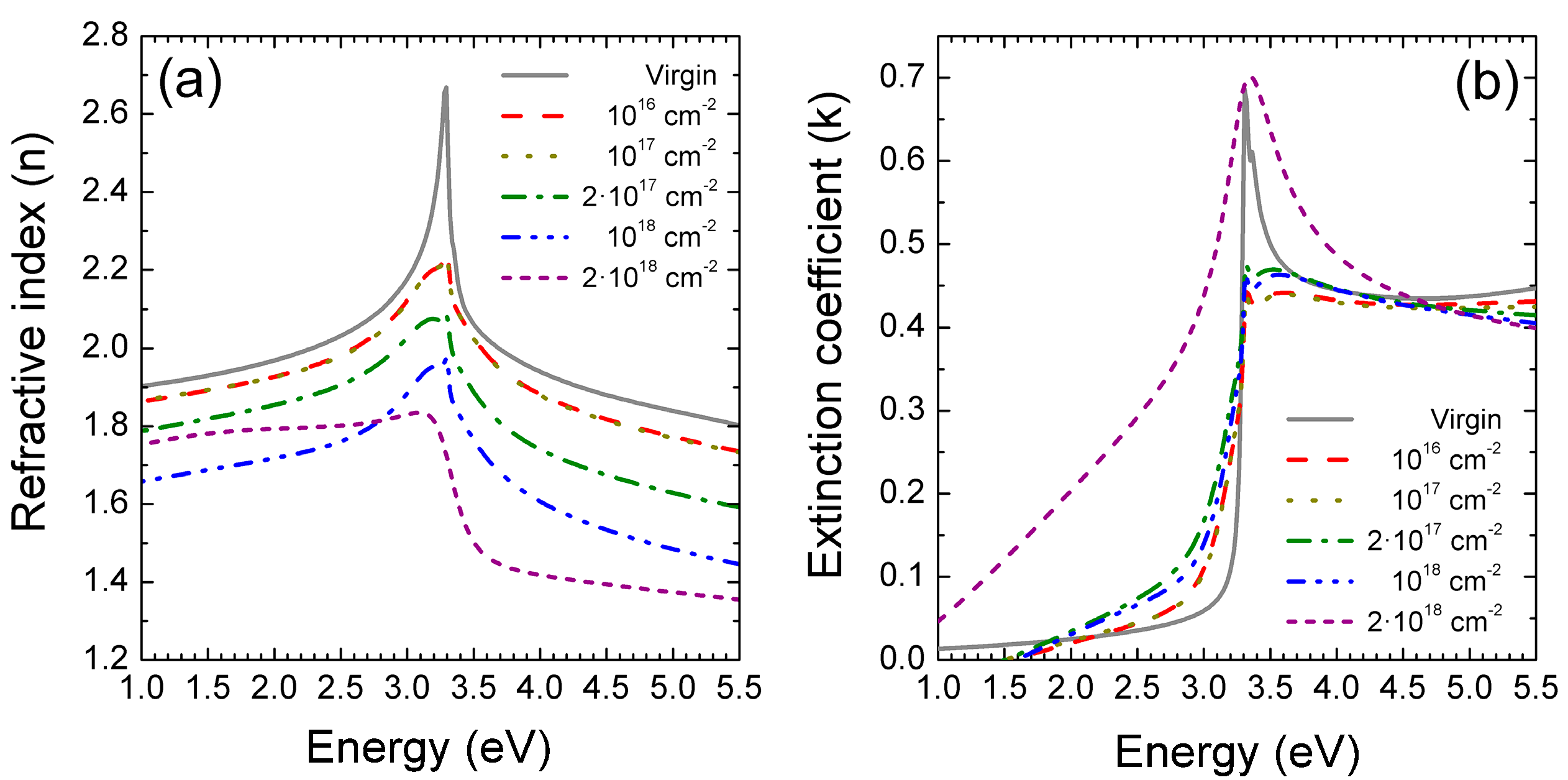
Figure 7 depicts the optical constants (refractive index and extinction coefficient) extracted from the analysis of the ZnO damaged layer for the different Ar+ fluences. It can be clearly seen that the refractive index (n) of the ZnO damaged layer decreases by increasing the fluence, indicating a decrease in the optical density of the material. Note that for low fluences (1016 and 1017 cm−2), the optical constants are essentially identical, indicating a similar damage level for this regime. Interestingly, the obtained refractive index values of the ZnO damaged layer are above the refractive index values of amorphous ZnO [45]. For instance, at 1.5 eV, the refractive index of amorphous ZnO is 1.48 [45], indicating that the damaged ZnO layers are not completely amorphized, in good agreement with the MEIS measurements which do not show a fully amorphous layer.
Regarding the extinction coefficient (k), there is a clear change due to the absorption below the bandgap (for energies lower than 3.2 eV). Indeed, this absorption is enhanced with the increase of the fluence, confirming an increase in the density of irradiation-induced defects (i.e., a higher number of states in the bandgap obtained for the highest fluence), accompanied by a redshift of ECPPB as seen from the absorption below the ZnO bandgap. This enhanced absorption below the bandgap due to irradiation or implantation-induced defects has already been reported in other wide-bandgap semiconductors such as III-nitrides [46,47].
4. Conclusions
In this work, we demonstrated the formation of ripple nanopatterns on bulk ZnO crystals by means of irradiation with 20 keV Ar+ ions. The ripple dynamics follows a power law dependence for both the roughness and the wavelength. At high fluences (~1018 cm−2) these ripples show coarsening accompanied by a strong change in the slope distribution. In this regime, the ripple front also seems to be independent of the beam direction, which suggests the presence of mechanisms complementary to ion erosion such as an Erlich-Schwoebel (E-S) barrier. A 3-layer SE optical model was used to model the damage and the roughness evolution of the samples. The dispersion model employed to describe the irradiated ZnO samples provides a good fit to the experimental data. According to the model, the thickness of the damaged layer is ~40 nm for all of the samples, with an increase in roughness, which is in good agreement with AFM data. The optical constants of the damaged ZnO layer exhibit two main optical features: a reduction of the refractive index with fluence, indicating a decrease in the optical density of the material, and an enhanced absorption below the bandgap. The irradiated samples were not completely amorphized, even at large fluences, confirming the radiation resistance of the material.
Author Contributions
Conceptualization, A.R.-C., L.V., K.L., and N.B.S.; methodology, A.R.-C., N.B.S.; software, A.R.-C., L.V., D.J., and N.B.S.; validation, A.R.-C., L.V. and N.B.S.; formal analysis, A.R.-C., L.V., D.J., and N.B.S.; investigation, A.R.-C., L.V., D.J., K.L. and N.B.S.; resources, L.V., D.J., and K.L.; data curation, A.R.-C., L.V., and N.B.S.; writing—original draft preparation, A.R.-C., L.V., and N.B.S.; writing—review and editing, A.R.-C., L.V., D.J., K.L. and N.B.S.; visualization, A.R.-C., L.V., N.B.S.; supervision, A.R.-C. and N.B.S.; project administration, A.R.-C., K.L., L.V. and N.B.S.; funding acquisition, A.R.-C., K.L., L.V. and N.B.S.
Funding
This research is supported by MINECO (CTQ2017-84309-C2-2-R) and Comunidad de Madrid (NANOAVANSENS ref. S2018/NMT-4349) projects, and the Ramón y Cajal program (RYC-2015-18047). This research is also funded by FEDER funds through the POR Lisboa, COMPETE 2020 Programme and National funds through FCT - Portuguese Foundation for Science and Technology (FCT) under the projects UID/CTM/50025/2019, POCI-01-0145-FEDER-028011 & LISBOA-01-0145-FEDER-029666.
Acknowledgments
We thank Jorge Rocha for his technical help with the ion implantations. We thank T. Monteiro and J. Rodrigues for fruitful discussions.
Conflicts of Interest
The authors declare no conflict of interest.
References
- Muñoz-García, J.; Vázquez, L.; Castro, M.; Gago, R.; Redondo-Cubero, A.; Moreno-Barrado, A.; Cuerno, R. Self-organized nanopatterning of silicon surfaces by ion beam sputtering. Mater. Sci. Eng. R-Rep. 2014, 86, 1–44. [Google Scholar] [CrossRef] [Green Version]
- Facsko, S.; Dekorsy, T.; Koerdt, C.; Trappe, C.; Kurz, H.; Vogt, A.; Hartnagel, H.L. Formation of ordered nanoscale semiconductor dots by ion sputtering. Science 1999, 285, 1551–1553. [Google Scholar] [CrossRef] [PubMed]
- Frost, F.; Schindler, A.; Bigl, F. Roughness Evolution of ion sputtered rotating InP surfaces: pattern formation and scaling laws. Phys. Rev. Lett. 2000, 85, 4116–4119. [Google Scholar] [CrossRef] [PubMed]
- Frost, F.; Ziberi, B.; Höche, T.; Rauschenbach, B. The shape and ordering of self-organized nanostructures by ion sputtering. Nucl. Instr. Meth. B 2004, 216, 9–19. [Google Scholar] [CrossRef]
- Facsko, S.; Kurz, H.; Dekorsy, T. Energy dependence of quantum dot formation by ion sputtering. Phys. Rev. B 2001, 63, 1–5. [Google Scholar] [CrossRef]
- Wendler, E.; Wesch, W.; Azarov, A.Y.; Catarino, N.; Redondo-Cubero, A.; Alves, E.; Lorenz, K. Comparison of low- and room-temperature damage formation in Ar ion implanted GaN and ZnO. Nucl. Instrum. Meth. B 2003, 307, 394–398. [Google Scholar] [CrossRef]
- Nakamura, S.; Pearton, S.; Fasol, G. The Blue Laser Diode; Springer: Berlin, Germany, 1997. [Google Scholar]
- Nakahara, K.; Akasaka, S.; Yuji, H.; Tamura, K.; Fujii, T.; Nishimoto, Y.; Takamizu, D.; Sasaki, A.; Tanabe, T.; Takasu, H.; et al. Nitrogen doped MgxZn1−xO/ZnO single heterostructure ultraviolet light-emitting diodes on ZnO substrates. Appl. Phys. Lett. 2010, 97, 1–3. [Google Scholar] [CrossRef]
- Qian, H.X.; Zhou, W. Focused ion beam irradiation of ZnO film: an atomic force microscopy study. J. Phys. D: Appl. Phys. 2009, 42, 1–5. [Google Scholar] [CrossRef]
- Jia, X.; Jia, T.Q.; Zhang, Y.; Xiong, P.X.; Feng, D.H.; Sun, Z.R.; Qiu, J.R.; Xu, Z.Z. Periodic nanoripples in the surface and subsurface layers in ZnO irradiated by femtosecond laser pulses. Optics Lett. 2010, 35, 1248–1250. [Google Scholar] [CrossRef]
- Bhattacharjee, S.; Karmakar, P.; Sinha, A.K.; Charkrabarti, A. Ripple topography on thin ZnO films by grazing and oblique incidence ion sputtering. Appl. Surf. Sci. 2011, 257, 6775–6778. [Google Scholar] [CrossRef]
- Petrik, P.; Polgár, O.; Fried, M.; Lohner, T.; Khánh, N.Q.; Gyulai, J. Ellipsometric characterization of damage profiles using an advanced optical model. J. Appl. Phys. 2003, 93, 1987–1990. [Google Scholar] [CrossRef]
- Erman, M.; Theeten, J.B.; Chambon, P.; Kelso, S.M.; Aspnes, D.E. Optical properties and damage analysis of GaAs single crystals partly amorphized by ion implantation. J. Appl. Phys. 1984, 56, 2664–2671. [Google Scholar] [CrossRef]
- Ziegler, J.F.; Biersack, J.P.; Littmark, U. The Stopping and Range of Ions in Solids. In Ion Implantation Techniques; Heiner, R., Hans, G., Eds.; Pergamon: New York, NY, USA, 1985. [Google Scholar]
- Nečas, D.; Klapetek, P. Gwyddion: an open-source software for SPM data analysis. Cent. Eur. J. Phys. 2012, 10, 181–188. [Google Scholar] [CrossRef]
- Abramoff, M.D.; Magalhaes, P.J.; Ram, S.J. Image processing with ImageJ. Biophotonics Int. 2004, 11, 36–42. [Google Scholar]
- Azzam, R.M.A.; Bashara, N.M. Ellipsometry and Polarized Light; 3rd reprint 1999 Edition; North Holland: Amsterdam, The Netherlands, 1977. [Google Scholar]
- Fujiwara, H. Spectroscopic Ellipsometry: Principles and Applications. Wiley: Chichester, UK, 2007. [Google Scholar]
- Barabási, A.L.; Stanley, H.E. Fractal Concepts in Surface Growth; Cambridge University Press: Cambridge, UK, 1995. [Google Scholar]
- Chan, W.L.; Chason, E. Making waves: kinetic processes controlling surface evolution during low energy ion sputtering. J. Appl. Phys. 2007, 101, 1–46. [Google Scholar] [CrossRef]
- Vasco, E.; Zaldo, C.; Vazquez, L. Growth evolution of ZnO films deposited by pulsed laser ablation. J. Phys.: Condens. Matter 2001, 13, L663–L672. [Google Scholar] [CrossRef]
- Baxter, J.B.; Wu, F.; Aydil, E.S. Growth mechanism and characterization of zinc oxide hexagonal columns. Appl. Phys. Lett. 2003, 83, 3797–3799. [Google Scholar] [CrossRef]
- Engler, M.; Macko, S.; Frost, F.; Michely, T. Evolution of ion beam induced patterns on Si(001). Phys. Rev. B. 2014, 89, 1–14. [Google Scholar] [CrossRef]
- Vivo, E.; Nicoli, M.; Engler, M.; Michely, T.; Vázquez, L.; Cuerno, R. Strong anisotropy in surface kinetic roughening: analysis and experiments. Phys. Rev. B 2012, 86, 1–8. [Google Scholar] [CrossRef]
- López, J.M.; Rodríguez, M.A.; Cuerno, R. Superroughening versus intrinsic anomalous scaling of surfaces. Phys. Rev. E 1997, 56, 3993–3998. [Google Scholar] [CrossRef] [Green Version]
- Auger, M.A.; Vázquez, L.; Sánchez, O.; Jergel, M.; Cuerno, R.; Castro, M. Growth dynamics of reactive-sputtering-deposited AlN films. J. Appl. Phys. 2005, 97, 123528. [Google Scholar] [CrossRef] [Green Version]
- Auger, M.A.; Vázquez, L.; Cuerno, R.; Castro, M.; Jergel, M.; Sánchez, O. Intrinsic anomalous surface roughening of TiN films deposited by reactive sputtering. Phys. Rev. B 2006, 73, 1–7. [Google Scholar] [CrossRef]
- Chowdhury, D.; Ghose, D. Super-roughening scaling behaviour of Si surface morphology at grazing incidence low energy ion beam sputtering. Appl. Surf. Sci. 2015, 324, 517–524. [Google Scholar] [CrossRef]
- Keller, A.; Cuerno, R.; Facsko, S.; Möller, W. Anisotropic scaling of ripple morphologies on high-fluence sputtered silicon. Phys. Rev. B 2009, 79, 1–7. [Google Scholar] [CrossRef]
- Cuerno, R.; Castro, M.; Muñoz-García, J.; Gago, R.; Vázquez, L. Universal non-equilibrium phenomena at submicrometric surfaces and interfaces. Eur. Phys. J. Special Topics 2007, 146, 427–441. [Google Scholar] [CrossRef]
- Krug, J. Origins of scale invariance in growth processes. Adv. Phys. 1997, 46, 139–282. [Google Scholar] [CrossRef]
- Rezakhaniha, R.; Agianniotis, A.; Schrauwen, J.T.C.; Griffa, A.; Sage, D.; Bouten, C.V.C.; van de Vosse, F.N.; Unser, M.; Stergiopulos, N. Experimental investigation of collagen waviness and orientation in the arterial adventitia using confocal laser scanning microscopy. Biomech. Model. Mechanobiol. 2012, 11, 451–473. [Google Scholar] [CrossRef]
- Fried, M.; Lohner, T.; Gyulai, J. Ellipsometric analysis. In Effect of Disorder and Defects in Ion-Implanted Semiconductors: Optical and Photothermal Characterization; Christofides, C., Ghibaudo, G., Semiconductor and Semimetals, Eds.; Academic Press: San Diego, CA, USA, 1997. [Google Scholar]
- Ben Sedrine, N.; Zukauskaite, A.; Birch, J.; Jensen, J.; Hultman, L.; Schöche, S.; Schubert, M.; Darakchieva, V. Infrared dielectric functions and optical phonons of wurtzite YxAl1−xN (0 ≤ x ≤ 0.22). J. Phys. D Appl. Phys. 2015, 48, 1–8. [Google Scholar] [CrossRef]
- Tanguy, C. Optical dispersion by Wannier excitons. Phys. Rev. Lett. 1995, 75, 4090–4093. [Google Scholar] [CrossRef] [PubMed]
- Bouzarâa, M.B.; Battie, Y.; Dalmasso, S.; Zaïbi, M.A.; Oueslati, M.; En Naciri, A. Comparative study of ZnO optical dispersion laws. Superlattices Microstruct. 2017, 104, 24–36. [Google Scholar] [CrossRef]
- Jellison, G.E.; Modine, F.A. Parameterization of the optical functions of amorphous materials in the interband region. Appl. Phys. Lett. 1996, 69, 371–373. [Google Scholar] [CrossRef]
- Jellison, G.E.; Modine, F.A. Erratum. Appl. Phys. Lett. 1996, 69, 2137. [Google Scholar] [CrossRef]
- Aspnes, D.E. Optical properties of solids. In Handbook on Semiconductors; Balkanski, E.M., Ed.; North Holland: Amsterdam, The Netherlands, 1980. [Google Scholar]
- Bruggeman, A.G. Berechnung verschiedener physikalischer Konstanten von heterogenen Substanzen. I. Dielektrizitätskonstanten und Leitfähigkeiten der Mischkörper aus isotropen Substanzen. Ann. Phys. (Leipzig) 1935, 24, 636–664. [Google Scholar] [CrossRef]
- Levenberg, K. A method for the solution of certain problems in least squares. Q. J. Math. 1944, 2, 164–168. [Google Scholar]
- Marquardt, D.W. An algorithm for least-squares estimation of nonlinear parameters. J. Soc. Ind. Appl. Math. 1963, 11, 431–441. [Google Scholar] [CrossRef]
- Ben Sedrine, N.; Lafosse, X.; Mauguin, O.; Chtourou, R.; Harmand, J.C. Rapid thermal annealing effects on the optical properties of GaAs0.9−xNxSb0.1 structures grown by MBE. Mater. Sci. Semicond. Process. 2015, 29, 331–336. [Google Scholar] [CrossRef]
- Shrisha, B.V.; Bhat, S.; Kushavah, D.; Naik, K.G. Hydrothermal growth and characterization of Al-doped ZnO nanorods. Mater. Today Proc. 2016, 3, 1693–1701. [Google Scholar] [CrossRef]
- Ghodsi, F.E.; Absalan, H. Comparative study of ZnO thin films prepared by different sol-gel route. Acta Phys. Pol. A 2010, 118, 659–664. [Google Scholar] [CrossRef]
- Ben Sedrine, N.; Rodrigues, J.; Cardoso, J.; Faye, D.N.; Fialho, M.; Magalhães, S.; Martins, A.F.; Neves, A.J.; Alves, E.; Bockowski, M.; et al. Optical investigations of europium ion implanted in nitride-based diode Structures. Surf. Coat. Technol. 2018, 355, 40–44. [Google Scholar] [CrossRef]
- Ben Sedrine, N.; Rodrigues, J.; Faye, D.N.; Neves, A.J.; Alves, E.; Bockowski, M.; Hoffmann, V.; Weyers, M.; Lorenz, K.; Correia, M.R.; et al. Eu-Doped AlGaN/GaN superlattice-based diode structure for red lighting: excitation mechanisms and active sites. ACS Appl. Nano Mater. 2018, 1, 3845–3858. [Google Scholar] [CrossRef]
Figure 1.
Atomic force microscopy (AFM) images of ZnO samples irradiated at 60° for different Ar fluences: (a) virgin, (b) 1016, (c) 1017, (d) 2 × 10¹⁷, (e) 1018, (f) 2 × 1018 cm−2. The ion beam direction runs vertically from the bottom of the images. The insets of (e,f) show zoomed regions where the derivative along the x-axis was performed in order to highlight the tiny elongated structures aligned along the ion beam direction on the ripple structures. The horizontal bars indicate 200 nm and 500 nm in (e,f), respectively.
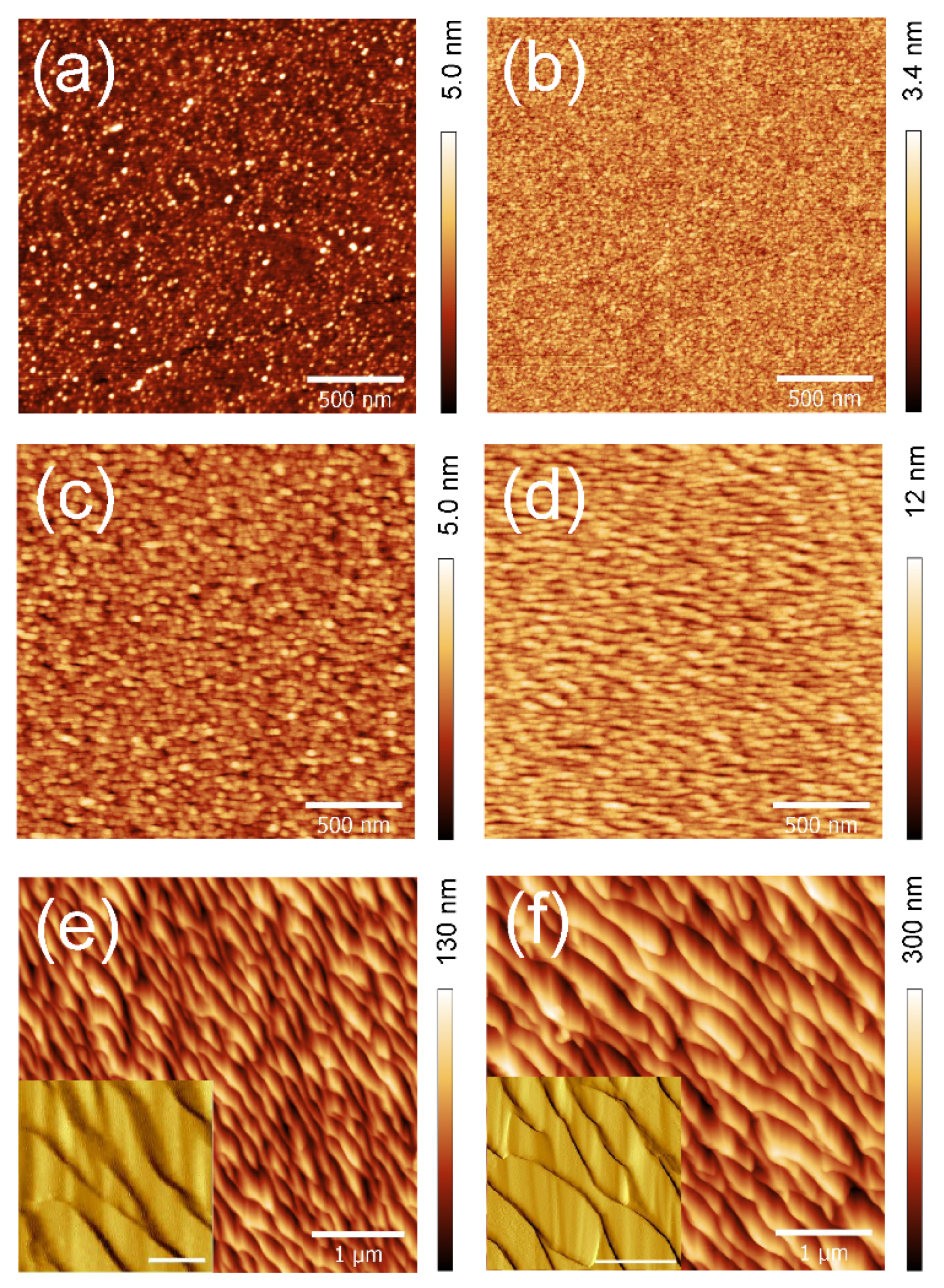
Figure 2.
(a) Power spectral density (PSD) functions obtained along the x-axis (for the virgin and low fluence irradiated surfaces) and along the perpendicular direction of the ripple pattern (for the higher fluences). The dashed line indicates the linear regime for the high k range. From its slope, a value of the exponent α = 2.1 is obtained. (b) Logarithmic plot of the surface roughness versus the fluence. The dashed line corresponds to the power law dependence observed with exponent β = 1.6. Inset: logarithmic plot of the pattern wavelength for the three samples displaying a ripple pattern. The dashed line corresponds to the power law dependence with a coarsening exponent 1/z = 0.6.

Figure 3.
(a,b) SEM images taken on the samples irradiated at 1018 cm−2 and 2 × 1018 cm−2, respectively. (c) Surface angle distribution obtained from the AFM images for the irradiated samples. (d) Normalized ripple orientation angle distribution obtained from the corresponding SEM images, except for the lowest fluence case where it was obtained from the AFM data.
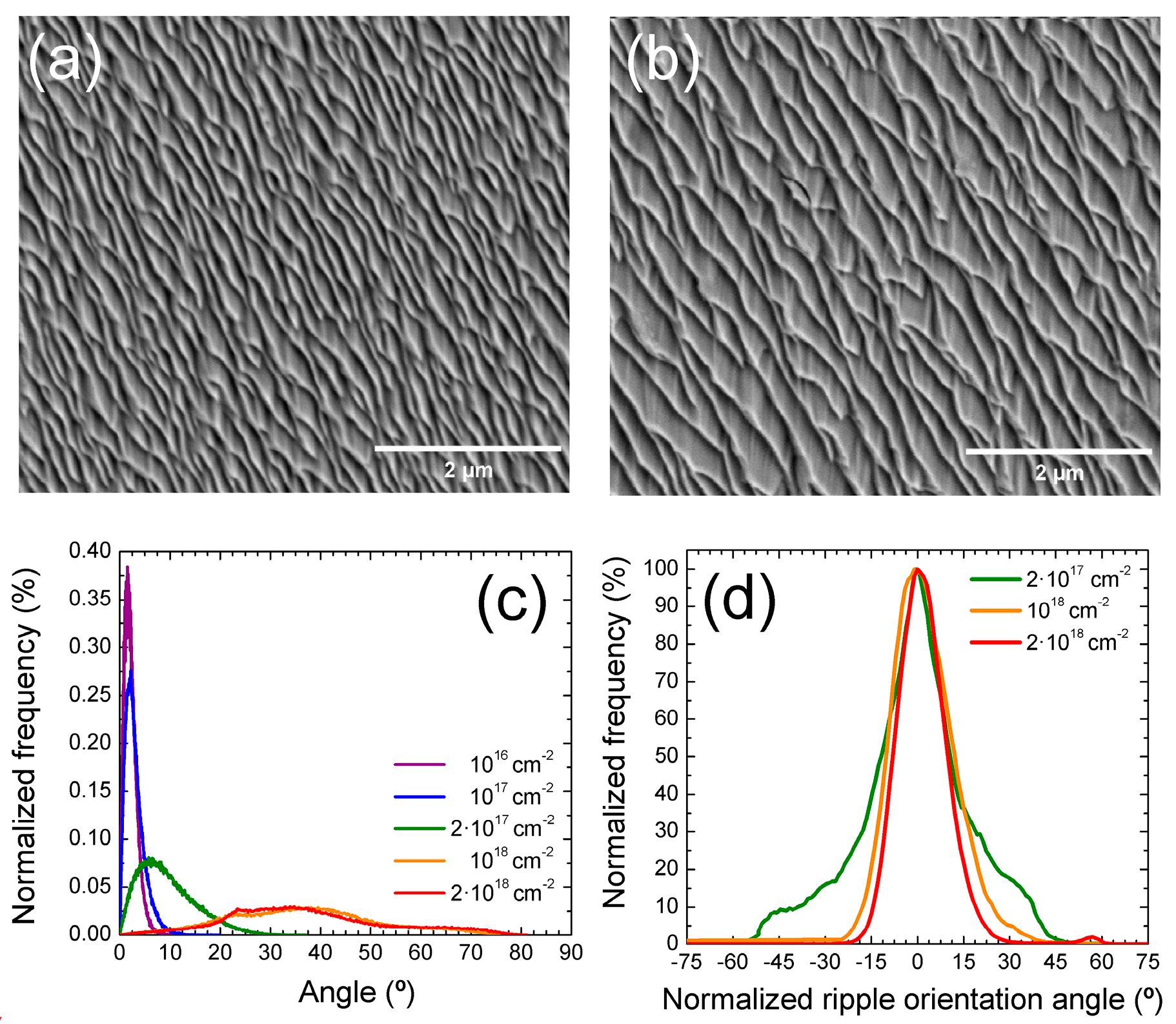
Figure 4.
Random and aligned medium energy ion scattering (MEIS) spectra of the ZnO sample irradiated at the highest fluence (2 × 1018 cm−2). The solid line shows the fit for the random spectrum.
Figure 4.
Random and aligned medium energy ion scattering (MEIS) spectra of the ZnO sample irradiated at the highest fluence (2 × 1018 cm−2). The solid line shows the fit for the random spectrum.

Figure 5.
Physical model for spectroscopic ellipsometry (SE) representing the nanopatterned ZnO samples.
Figure 5.
Physical model for spectroscopic ellipsometry (SE) representing the nanopatterned ZnO samples.

Figure 6.
Experimental data (dots) and best fits (lines) for ψ (a) and Δ (b) ellipsometric parameters of the ZnO irradiated samples at the different studied fluences.
Figure 6.
Experimental data (dots) and best fits (lines) for ψ (a) and Δ (b) ellipsometric parameters of the ZnO irradiated samples at the different studied fluences.
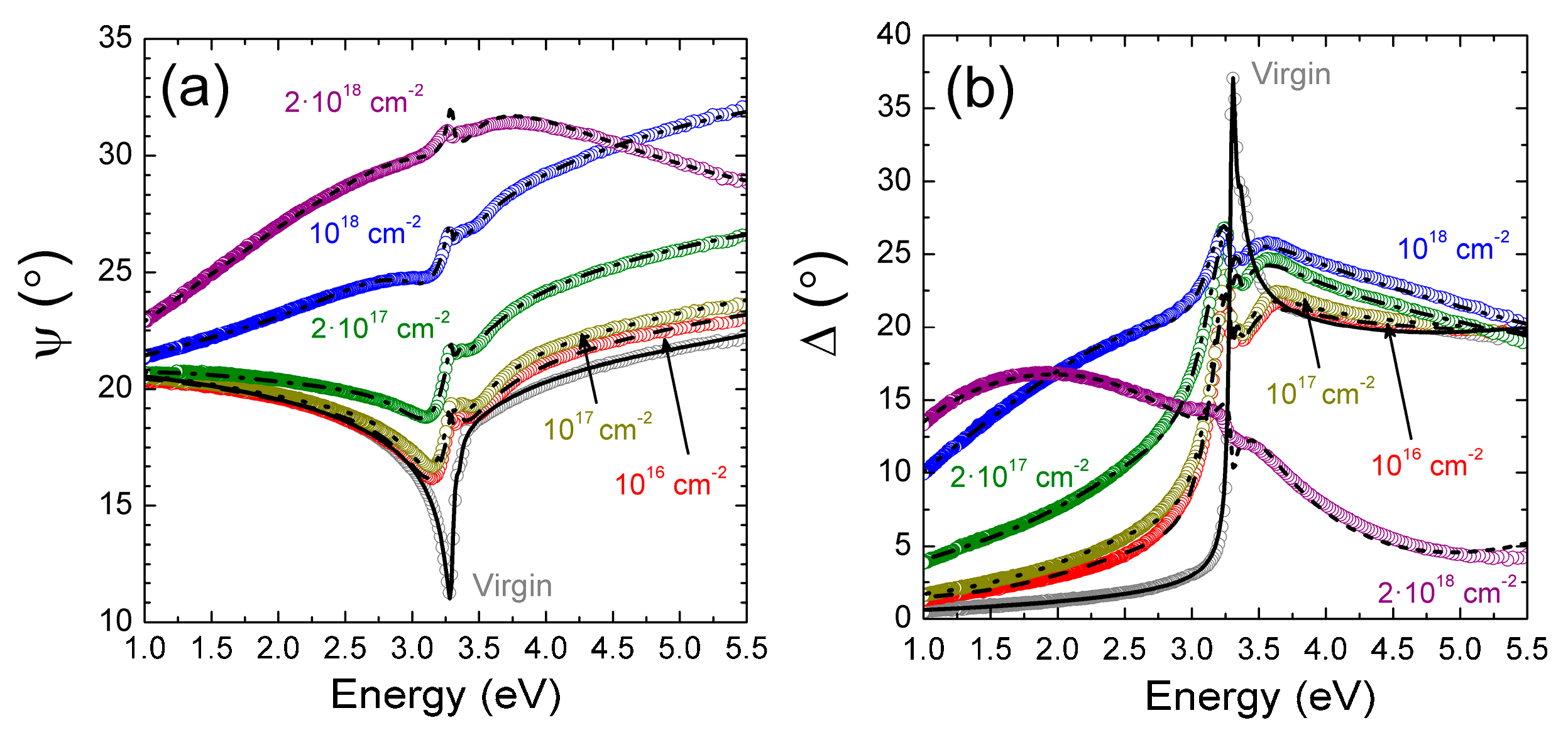
Figure 7.
Refractive index (a) and extinction coefficient (b) extracted from the ellipsometric model for the ZnO damaged layer at the different fluences. Note the complete overlapping of the optical constants at low fluences (curves for 1016 and 1017 cm−2).
Figure 7.
Refractive index (a) and extinction coefficient (b) extracted from the ellipsometric model for the ZnO damaged layer at the different fluences. Note the complete overlapping of the optical constants at low fluences (curves for 1016 and 1017 cm−2).

Table 1.
Parameters obtained from the best fits of the SE model: roughness (σ), thicknesses of the damaged layer (d), high-frequency limit dielectric constant (ε∞), and energy of the critical point (ECPPB). Errors in the last digit are indicated in parenthesis and correspond to the 90% confidence limits.
| Parameter | Ion Fluence | ||||
|---|---|---|---|---|---|
| 1016 cm−2 | 1017 cm−2 | 2 × 1017 cm−2 | 1018 cm−2 | 2 × 1018 cm−2 | |
| σSE (nm) | 0.09(2) | 1.55(3) | 2.0(4) | 15.3(6) | 82(3) |
| d (nm) | 38.8(2) | 39.7(1) | 43.5(3) | 51.6(3) | 36(1) |
| ε∞ | 1.165(3) | 1.16(6) | 1.14(5) | 0.90(2) | 0.8(3) |
| ECPPB (eV) | 2.9(3) | 2.7(3) | 2.4(3) | 2.1(3) | 1.5(3) |
© 2019 by the authors. Licensee MDPI, Basel, Switzerland. This article is an open access article distributed under the terms and conditions of the Creative Commons Attribution (CC BY) license (http://creativecommons.org/licenses/by/4.0/).
Share and Cite
MDPI and ACS Style
Redondo-Cubero, A.; Vázquez, L.; Jalabert, D.; Lorenz, K.; Ben Sedrine, N. Modelling of Optical Damage in Nanorippled ZnO Produced by Ion Irradiation. Crystals 2019, 9, 453. https://doi.org/10.3390/cryst9090453
AMA Style
Redondo-Cubero A, Vázquez L, Jalabert D, Lorenz K, Ben Sedrine N. Modelling of Optical Damage in Nanorippled ZnO Produced by Ion Irradiation. Crystals. 2019; 9(9):453. https://doi.org/10.3390/cryst9090453
Chicago/Turabian StyleRedondo-Cubero, Andrés, Luis Vázquez, Denis Jalabert, Katharina Lorenz, and Nebiha Ben Sedrine. 2019. "Modelling of Optical Damage in Nanorippled ZnO Produced by Ion Irradiation" Crystals 9, no. 9: 453. https://doi.org/10.3390/cryst9090453
Note that from the first issue of 2016, this journal uses article numbers instead of page numbers. See further details here.