Article

Advanced AlGaAs/GaAs Heterostructures Grown by MOVPE

by
Maxim A. Ladugin
1,*,
Irina V. Yarotskaya
1,
Timur A. Bagaev
1,
Konstantin Yu. Telegin
1,
Andrey Yu. Andreev
1,
Ivan I. Zasavitskii
2,
Anatoliy A. Padalitsa
1 and
Alexander A. Marmalyuk
1
1
Sigm Plus Co., 3 Vvedenskogo str., Moscow 117342, Russia
2
Lebedev Physical Institute, Russian Academy of Sciences, 53 Leninskii prosp., Moscow 119991, Russia
*
Author to whom correspondence should be addressed.
Crystals 2019, 9(6), 305; https://doi.org/10.3390/cryst9060305
Submission received: 21 April 2019 / Revised: 24 May 2019 / Accepted: 29 May 2019 / Published: 14 June 2019
(This article belongs to the Special Issue MOVPE Growth of Crystalline Film)

Abstract

:
AlGaAs/GaAs heterostructures are the base of many semiconductor devices. The fabrication of new types of devices demands heterostructures with special features, such as large total thickness (~20 μm), ultrathin layers (~1 nm), high repeatability (up to 1000 periods) and uniformity, for which a conventional approach of growing such heterostructures is insufficient and the development of new growth procedures is needed. This article summarizes our work on the metalorganic vapour-phase epitaxy (MOVPE) growth of AlGaAs/GaAs heterostructures for modern infrared devices. The growth approaches presented allow for the improved output characteristics of different emitting devices such as multi active region lasers, epitaxially integrated via highly doped tunnel junctions (emission wavelength λ ~ 1 μm), quantum cascade lasers (λ ~10 μm) and THz laser (λ ~100 μm), based on short-period superlattice with 500–2000 layers.

1. Introduction

AlGaAs/GaAs heterostructures are widely used in various electronic and optoelectronic applications [1,2]. The AlGaAs/GaAs material system is thoroughly investigated and traditionally considered to be ideal from the viewpoint of matching the lattice constants of the semiconductor substrate and epitaxial layers. This material system usually does not require any special technical procedures for mechanical stresses controlling during the growth of high-quality epitaxial layers for the conventional device heterostructures. However, despite the absence of misfit dislocations, these heterostructures suffer residual mechanical strains, which are lower than the threshold of formation of such dislocations. The strains mentioned may curve an epitaxial wafer, especially after substrate thinning in the post-growth processing, which is very critical for some practical applications. The interface quality of AlGaAs/GaAs heterostructures is acceptable, but the modern devices require controlling formation of ultrathin layers with high repeatability. This demands the development of new technical approaches for the creation of new types of semiconductor devices, even in the well-known AlGaAs/GaAs system.
In this work, several practical examples of metalorganic vapour-phase epitaxy (MOVPE) growth of such AlGaAs/GaAs heterostructures will be briefly discussed.

2. Experiment

All presented heterostructures were grown by low-pressure MOVPE in a horizontal quartz-reactor with a rotating graphite wafer susceptor. Growth temperature was varied from 550 °C to 800 °C, and reactor pressure was maintained in the range of 40–80 Torr. Sources of the group III elements were trimethylaluminum, trimethylgallium and triethylgallium; sources of the group V elements were arsine and phosphine. A mixture of silane in hydrogen as n-type and carbon tetrachloride and diethylzinc were used as p-type dopants. The carrier gas was hydrogen. The growth was carried out on epi-ready n-GaAs (100) substrates. Growth parameters were optimized to achieve high quality thin layers with abrupt heterointerfaces, appropriate doping profile, repeatability of periodic structures, strain control and high uniformity.
Grown heterostructures were studied by X-ray diffractometry (X-ray, Vektor, Nanometrics Incorporated, Milpitas, CA, USA), scanning electron microscopy (SEM, Vega3, Tescan, Brno - Kohoutovice, Czech Republic), transmission electron microscopy (TEM, JEM-2100F, JEOL Ltd., Tokyo, Japan) and photoluminescence (PL, RPM Sigma, Nanometrics Incorporated, Milpitas, CA, USA) measurements.

3. Results and Discussions

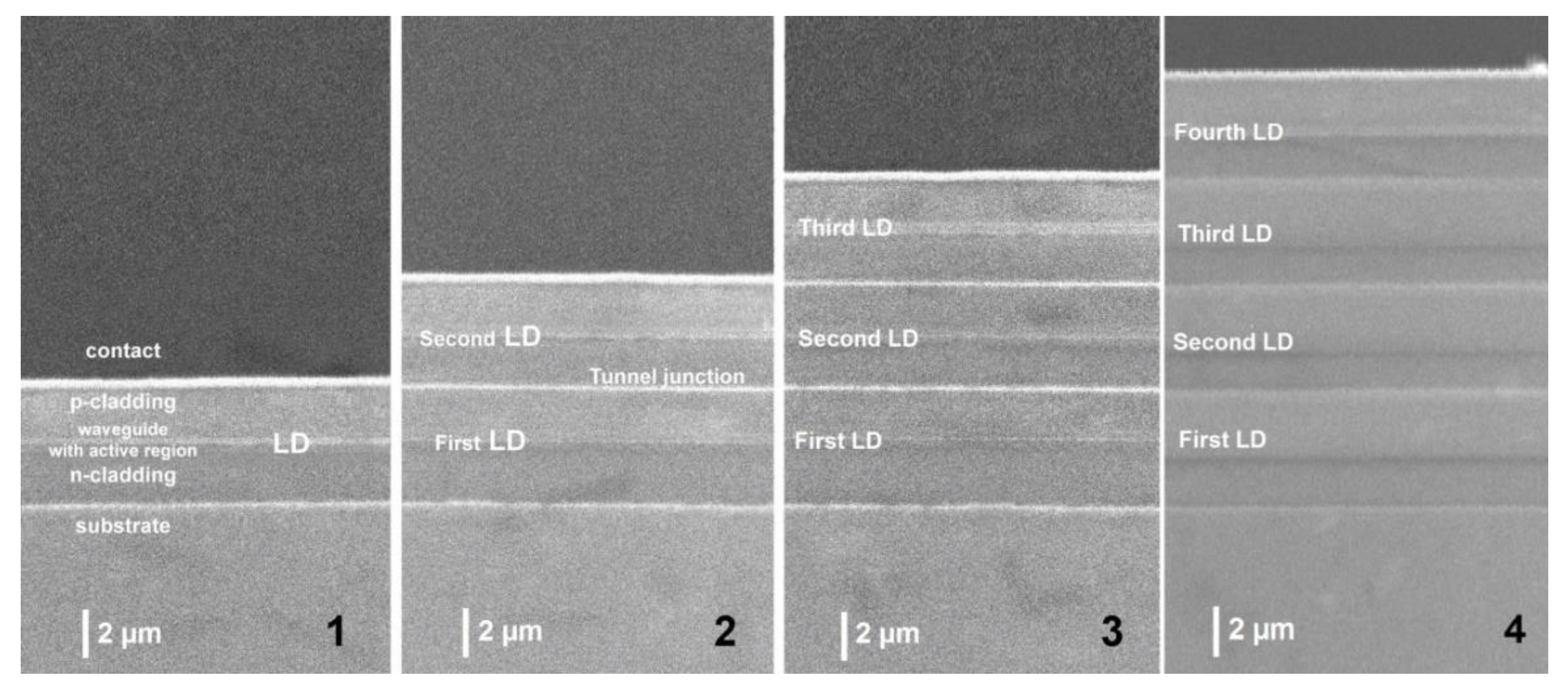
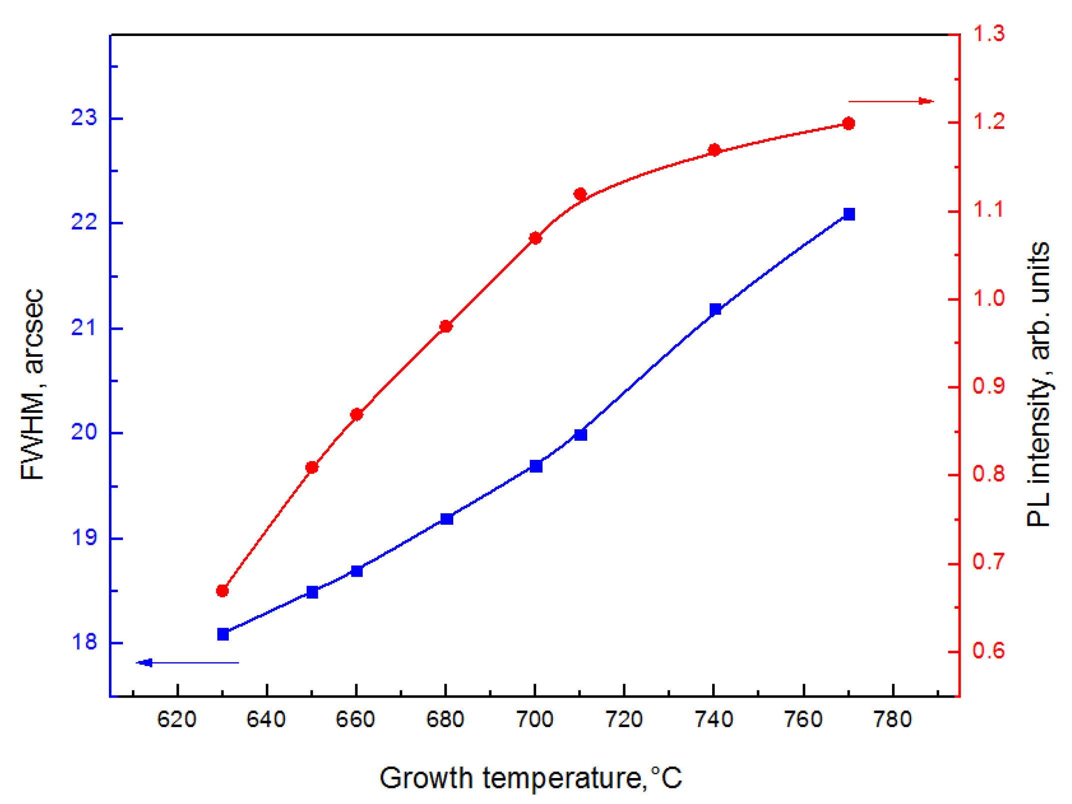
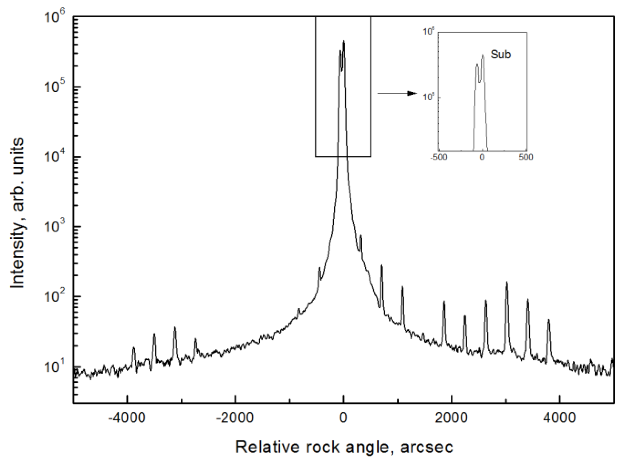
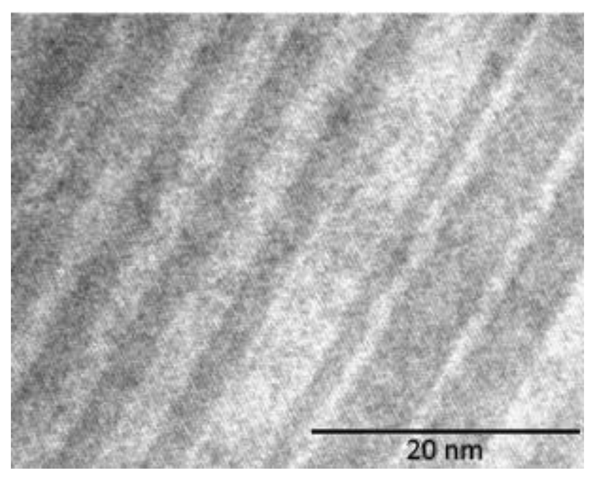
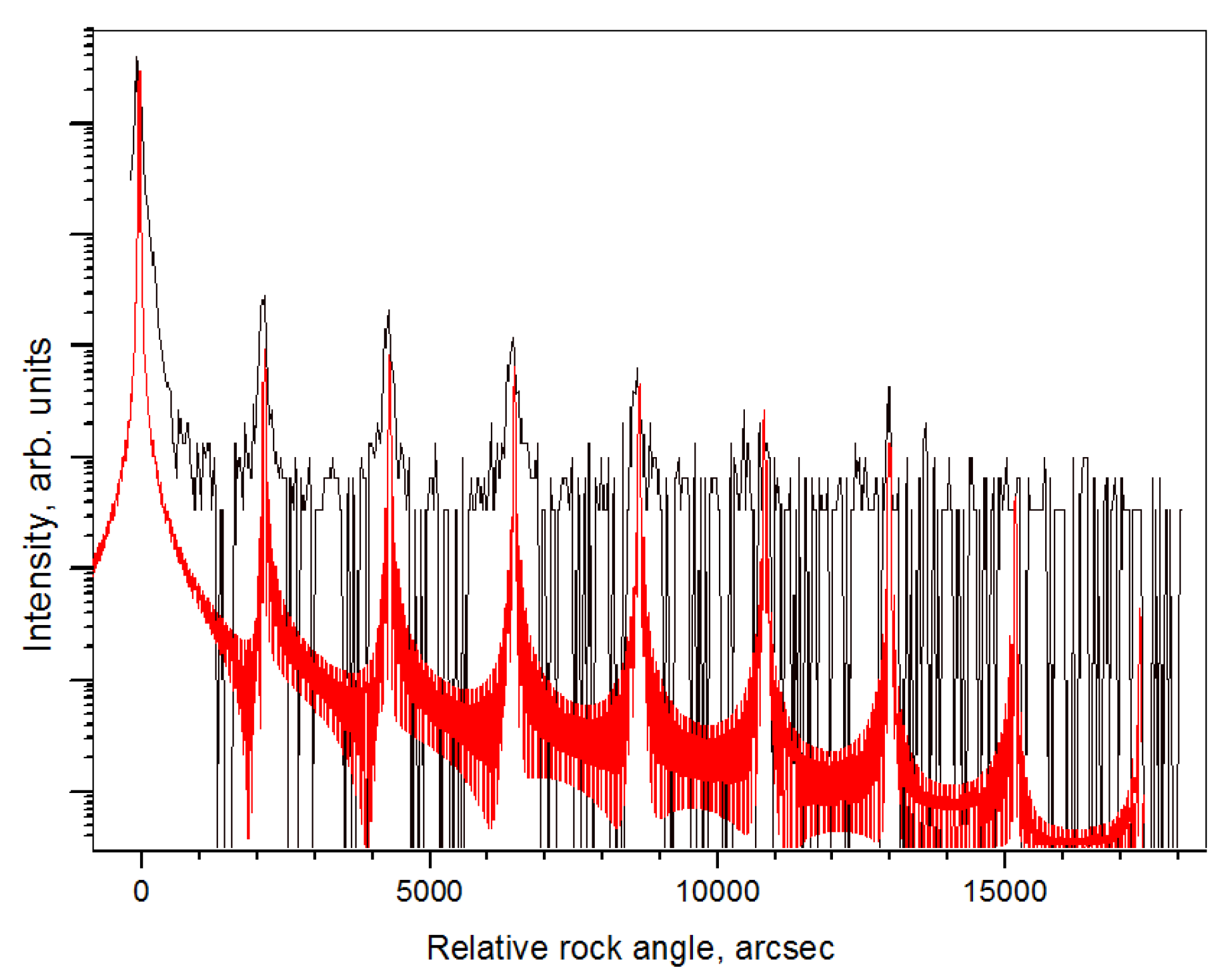
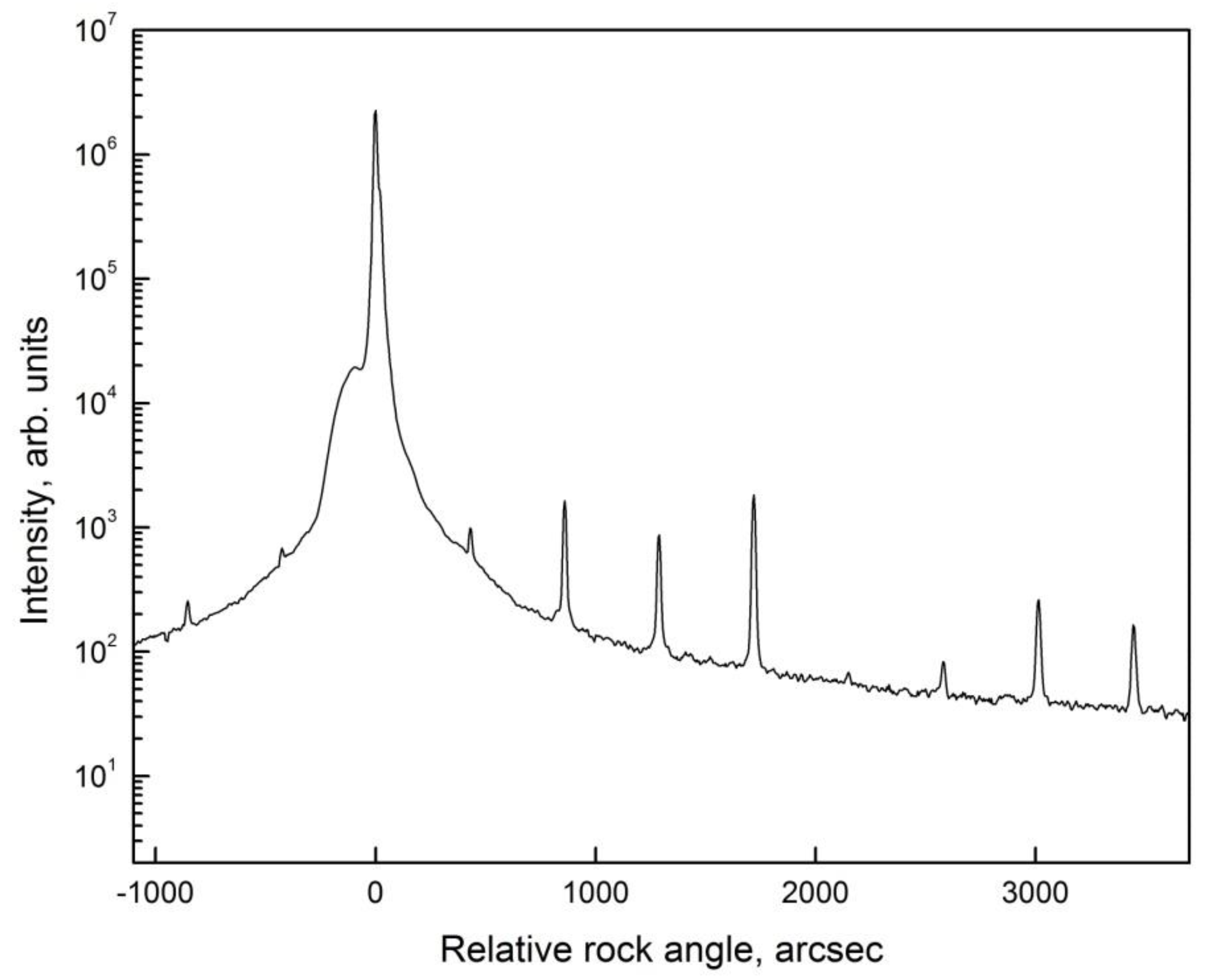
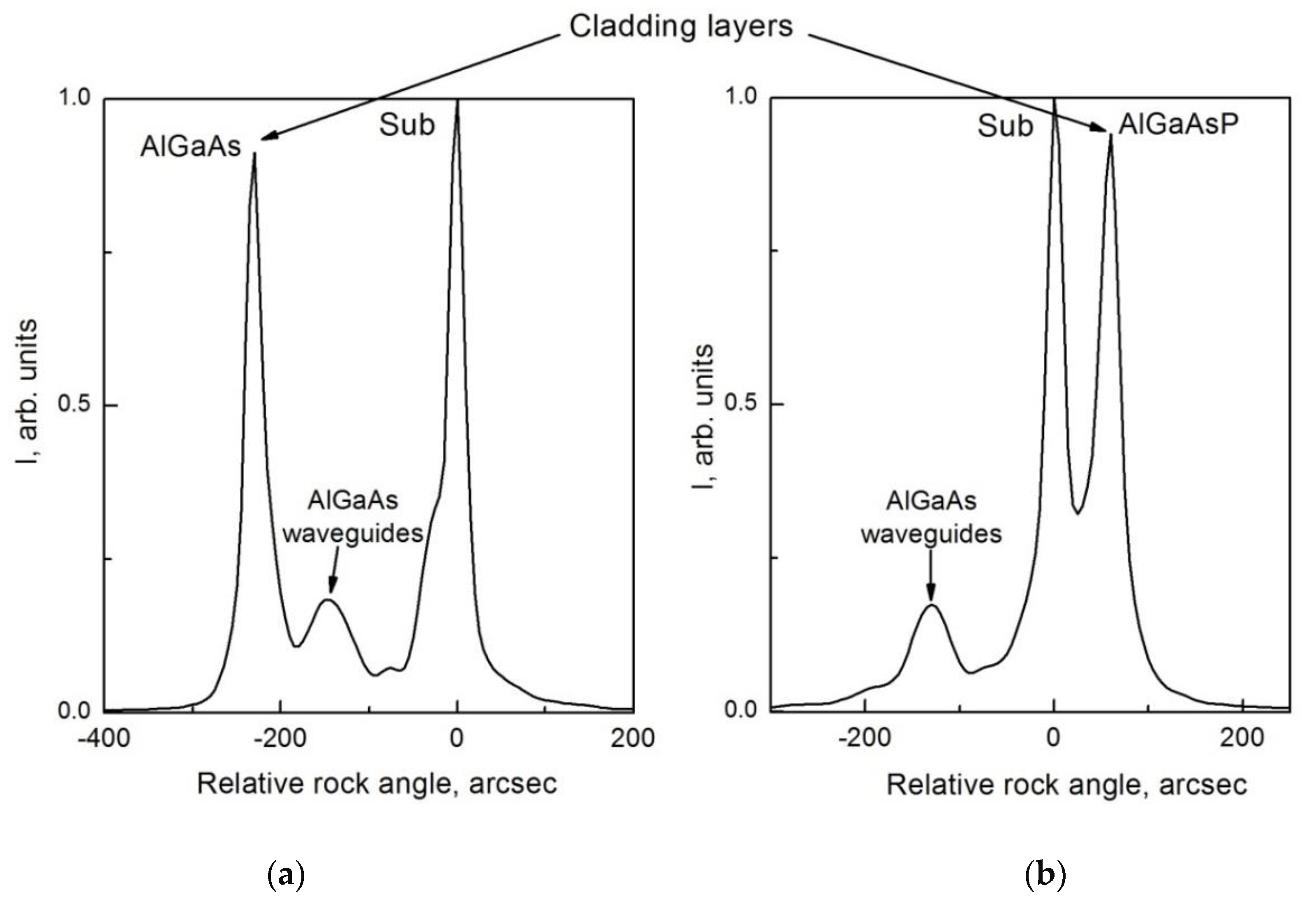
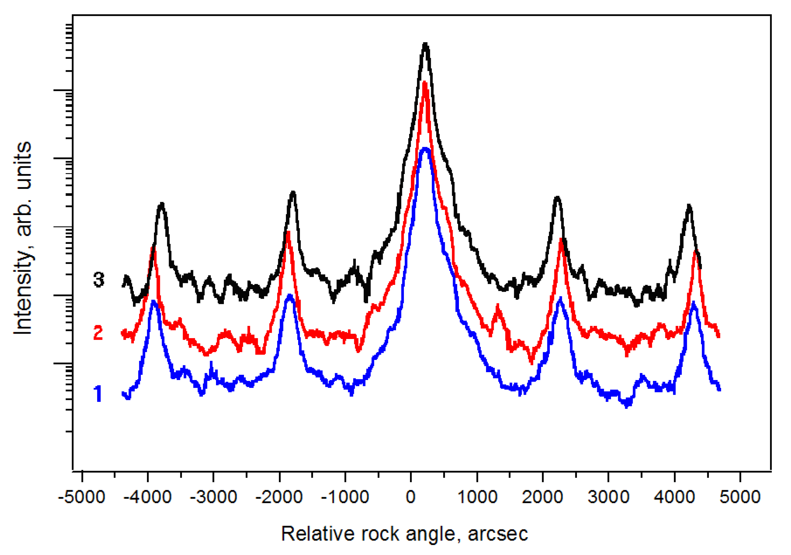
3.1. Heterostructures for Lasers Emitting at ~1 µm

Residual strains in the AlGaAs/GaAs heterostructures begin to play a notable role with an increase of the overall thickness (typically more than 10 microns), as illustrated by the following cases.
One of the possible ways to increase the output power of laser diodes (LDs) is the use of vertically integrated LDs grown in a single epitaxial process and connected by high-doped tunneling junctions. The principle of operation of an integrated laser was described in [3]. In the ideal case, any electron injected into the conduction band produces a number of photons equal to the number of LDs contained in the entire epitaxial structure, thereby increasing the output power. The external quantum efficiency of such devices can be considerably increased and can even exceed unity.
The first epitaxially-integrated laser heterostructures were grown by molecular beam and chemical beam epitaxies [4,5,6]. Recent developments in the MOVPE technology [7] made it possible to use this method for the growth of high-quality multilayered structures with different materials.
Such epitaxially-integrated laser structures based on AlGaAs/GaAs materials with two, three and four active regions emitting in the spectral ranges λ = 800–810, 890–910, and 1040–1060 nm were grown by the MOVPE. The integration (connection) of separate laser structures was performed using heavily doped tunneling junctions n+-GaAs:Si/p-GaAs:C; the features of obtaining such junctions are described in [8]. Microphotographs of the cross-section of the heterostructures with several emitting regions are shown in Figure 1. It is worth noting that the total thickness of epitaxially-integrated heterostructures containing three or four laser diodes was 13–16 μm; however, misfit dislocations were not yet formed in this case. Nevertheless, mechanical stress increased with the increase in total thickness, which resulted in epiwafer bowing.
By adjusting the content of the quantum wells (QWs) in the various emitting regions, it is possible to grow epitaxially-integrated laser with several wavelengths [9]. This approach has been used to grow double-stacked AlGaAs/GaAs heterostructures with different active regions, emitting at different wavelengths to realize multiwavelength lasers [10]. Single laser diodes, laser bars and arrays based on AlGaAs/GaAs heterostructures show a manifold increase in the differential quantum efficiency: lasers with two active regions by 1.8–2.0 times, with three—by 2.6–3.0 times, with four—by 3.4–4.0 times. Laser arrays made from these heterostructures can reach more than 1 kW of output power in a pulsed mode [11,12].
All grown heterostructures were studied by means of X-ray diffractometry, and the curvature radius was calculated [13]. Table 1 shows the results of the curvature radius calculation with the corresponding layer’s thickness and total lattice mismatch between the GaAs substrate and epitaxial layers for different samples. Depending on the difference in the lattice constants and the thicknesses of deposited layers, the wafer can be curved to one or another side and the curvature radius can be either positive or negative. The curvature radius is negative when the lattice parameter of the deposited layer is smaller than the substrate parameter. The lower the numerical value of the curvature radius, the larger curvature of the wafer.
Evidently, the curvature increases with the total thickness of AlGaAs/GaAs structures, and special methods of strain control are needed in such cases.
One of the possible methods for reducing residual strain in the AlGaAs/GaAs structures under consideration is the introduction of phosphorus into the alloys (AlGaPAs), in order to compensate the lattice constants difference between deposited layers and substrate [14,15].
Two types of laser heterostructures were studied: with Al0.60Ga0.40As cladding layers (conventional design) and Al0.60Ga0.40P0.03As0.97 cladding layers (compensated design). In the second case the molar fraction of phosphorus was calculated from mechanical strains in these heterostructures.
The curvature of the heterostructures was measured in-situ by optical reflectometry using an EpiCurveTT system (LayTec AG, Berlin, Germany); in addition, the structures were studied by means of X-ray diffractometry.
Figure 2 shows the X-ray rocking curves for the grown laser structures. One can clearly see that the peak corresponding to the cladding layer of the laser structure (CL peak) shifts with the addition of phosphorus. The lattice constant of the AlGaPAs cladding layer becomes smaller than the substrate lattice constant and the corresponding peak appears to the other side of the substrate peak (Sub). This occurred because the amount of added phosphorus was calculated taking into account that the strains must be compensated, not only in one layer, but also over the entire structure. Note that the waveguide layer composition was the same in both cases (Al0.37Ga0.63As—WG peak).
The calculated results of the curvature radius measured by means of optical reflectometry [16] are given in Table 2. The total thickness of deposited layers in both heterostructures was 4.75 μm. The mismatch and the curvature radius of the heterostructures with AlGaPAs layers are an order of magnitude better compared with the AlGaAs/GaAs sample. In our case, the curvature radius almost completely coincides with the initial curvature radius of the substrate equal to 72 m. This approach allows for the reduction of the total mechanical stresses and, consequently, to decrease the heterostructure curvature.
These structures were processed into laser bars. The AlGaPAs/GaAs structure demonstrated a flat near-field pattern and an improvement of the light–current characteristic at high pump currents because of a better thermal contact with the heat sink in comparison to the conventional AlGaAs/GaAs one [17].
The residual strain is not the only problem, which appears when growing a thick AlGaAs/GaAs structure with ultrathin layers. The interface abruptness, uniformity and repetitiveness are the most crucial aspects for the growth of the structures with a superlattice active region, especially for AlGaAs/GaAs superlattices with weak barriers.

3.2. Heterostructures for Lasers Emitting at ~10 µm

A quantum cascade laser (QCL) represents a more complicated structure than the one mentioned above. The active region of a QCL contains several QWs and barriers with an injector (slightly aperiodic, partially doped superlattice). The thickness of the layers forming QWs and barriers in the active region usually ranges from 1 to 5 nm, and the number of layers can reach 500 to 1000, depending on the number of cascades. Therefore, the use of precise epitaxial methods is needed for growing QCLs, so a molecular beam epitaxy was used to realize the first QCLs [18,19,20]. Later, MOVPE began to be used to grow some GaInAs/AlInAs laser heterostructures [21].
QCLs for the mid-IR spectral region (4–25 μm) are typically based on lattice-matched or strained GaInAs/AlInAs/InP heterostructures [22]. The AlGaAs/GaAs materials discussed here can be used to produce QCLs for the spectral region from 8 μm up to THz region (250 μm). AlGaAs alloys have a good lattice match to GaAs substrate in a wide range of composition. Moreover, only one group III element source is required to switch for producing a set of QWs and barriers (the number of heterojunctions in this QCL exceeds 500). This allows for the precise control of the ratio of components in the growth zone, and ensures stability of the composition of the QW and barrier layers, which is especially important in the case of QCLs. In a number of studies, AlGaAs/GaAs QCL heterostructures were grown by MOVPE [23]. To improve optical confinement in AlGaAs/GaAs QCLs, the authors in [24] used the In0.49Ga0.51P as cladding layers. In this paper, we report the MOVPE growth of QCL structure based on the GaAs/Al0.45Ga0.55As heterostructures.
For the efficient operation of QCLs, all of their periods should be identical in the thickness and profile of their QWs and barriers. The first few layers of the active region are exposed to high temperatures for 8–12 h, depending on process conditions, and the growth temperatures of AlGaAs materials are typically more than 700 °C, which may lead to the broadening of interfaces in the first few periods because of the diffusion of group III atoms [25,26]. The growth conditions of the epilayers in the QCL structure were optimized by varying the following parameters: the V/III ratio, the growth rate, the temperature and pressure in the reactor. To assess the quality of the thin layers, we carried out a series of experiments on the short-period superlattices (250 pairs of AlGaAs/GaAs layers 2.3 nm (Al0.45Ga0.55As barrier), and 3.7 nm (GaAs QW)) were grown and investigated. The growth temperature was lowered (from 770 to 630 °C) and the V/III ratio was varied (from 100 to 300). The superlattices were characterized by X-ray diffraction, TEM and PL spectroscopy. The typical diffraction curve is presented in Figure 3. The temperature dependencies of the FWHM (full width at half maximum) of the X-ray satellite peaks and the PL intensity of the interband transitions in the QWs are demonstrated in Figure 4. It can be seen that with decreasing temperature, the PL intensity falls off in the range 710–770 °C, with a small slope. Further lowering the temperature to 630 °C reduces the intensity by a factor of 2. At the same time, lowering the growth temperature led to a reduction in the width of satellite peaks, confirming a reduction in the diffusion-induced broadening of the barrier layer boundaries. Therefore, a compromise between optical and crystal quality is needed.
To grow a QCL AlGaAs/GaAs heterostructure consisting of three QWs and a typical active-region design with a diagonal optical transition and a single-phonon resonance, depopulation of the lower laser level was used [19].
The active region of the QCL heterostructure comprised 36 cascades, each consisting of alternating Al0.45Ga0.55As barrier layers and GaAs QWs (the thicknesses below are indicated in nanometers): 4.6/1.9/1.1/5.4/1.1/4.8/2.8/3.4/1.7/3.0/1.8/2.8/2.0/3.0/2.6/3.0. Here the barrier thicknesses are indicated in bold type and those of the doped layers are underlined. The active region was sandwiched between 2.5-μm-thick GaAs layers with a doping level of 4 × 1016 cm−3. The waveguide layers were sandwiched between two 0.5-μm-thick Al0.2Ga0.8As layers, in contrast to the waveguide design proposed previously by Page et al. [27]. The rocking curve clearly shows a large number of well-defined satellite peaks (Figure 5).
Analyzing the separation between the satellite peaks, the period of one cascade was determined. It was found to be 45.4 nm (at an intended value of 45.0 nm). The FWHM of the satellite peaks was in agreement with theoretical predictions (of the order of 20), indicating that there was no significant heterojunction broadening. From SEM measurements, the thickness of the active region was determined to be 1.63 μm, and the corresponding calculated period of one of the 36 cascades in the active region was 45.3 nm. Thus, these values agree with those evaluated from the diffraction curve.
According to the TEM measurements (Figure 6) the interfaces between the layers are equally well seen throughout the thickness of the active region, both at its beginning and at its end, indicating that the diffusion-induced broadening is rather small. Based on this type of heterostructure, a QCL with the following parameters was realized: the wavelength of 9.7 μm, the threshold current density of 2 kA/cm2 and emission power more than 0.2 W [28].

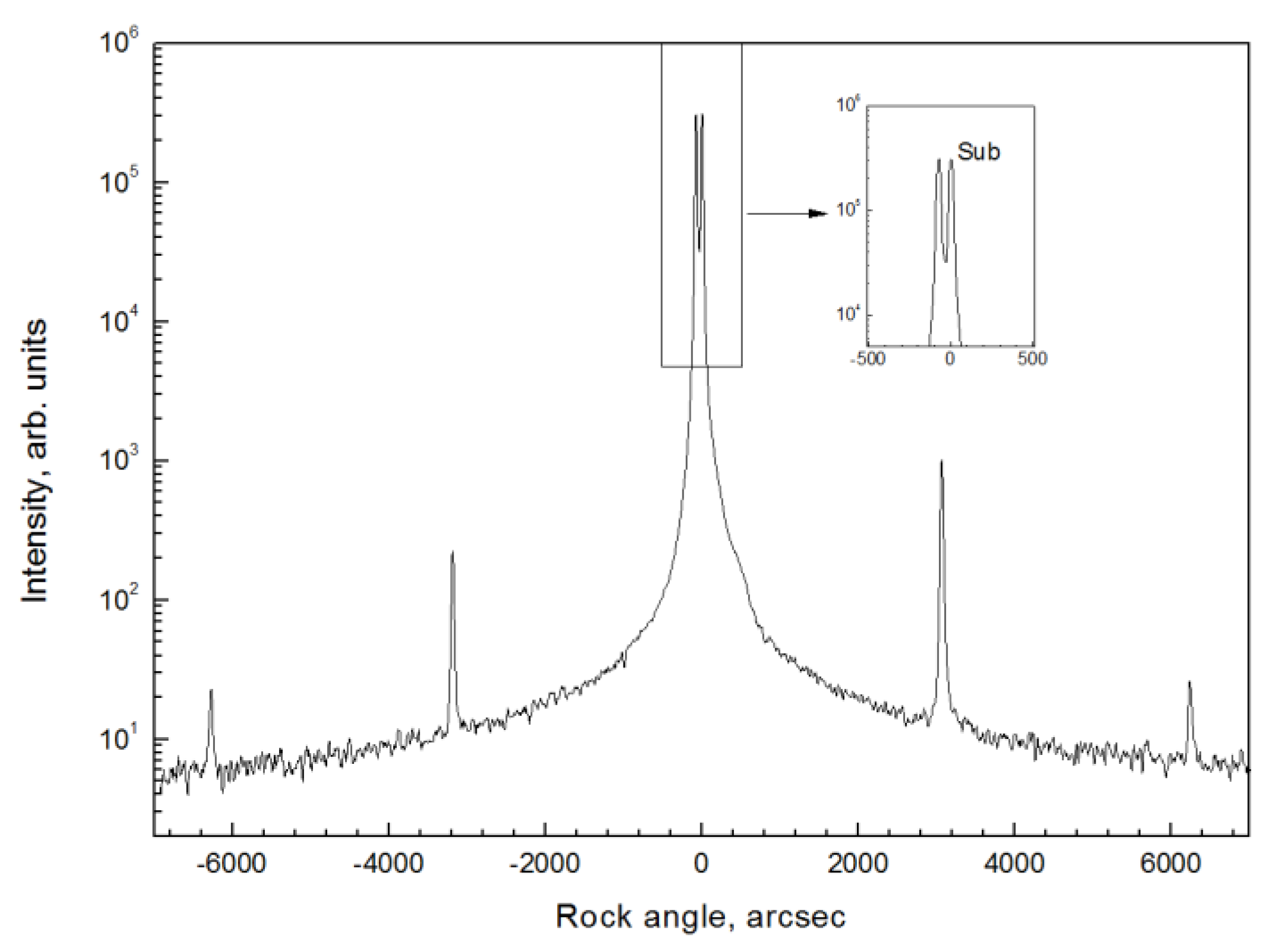
3.3. Heterostructures for Lasers Emitting at ~100 µm

To achieve optical transitions between two Wannier-Stark levels and suppress negative differential conductivity, the authors [29] simulated AlGaAs/GaAs superlattice with weak barriers (with low aluminum content). The active region for such a THz semiconductor laser contains more than 500 periods.
The major technological challenges during MOVPE growth of such heterostructures were to obtain high quality QWs and barriers with abrupt heterointerfaces, low doping levels in the active region and appropriate profile doping for cladding layers.
One of the main difficulties we faced was epitaxial growth of a very thick superlattice—more than 18 μm (1000 periods). In order to achieve this result, we had to optimize the growth regimes carefully for the best quality of the layers, keeping in mind that the time of the process was equal to 7–8 h.
A typical emitting structure consisted of two n-type cladding layers and superlattice as active region between them. For some technical operations, an etch-stop layer between the substrate and emitting structure was added. The superlattice had 1000 periods of GaAs layers (QWs) and AlGaAs barrier layers with 12–13% aluminum content. Thicknesses of QWs and barriers were determined by means of SEM, and X-ray measurements and were equal to 1.9–2.0 nm and 15.3–15.7 nm, respectively.
Figure 7 shows simulated and experimental X-ray curve for superlattice structure with DQW = 2 nm/Dbar = 15.5 nm.
To analyze uniformity and evaluate the possibilities of growth equipment, the different samples were grown and studied by means of X-ray diffraction. Figure 8 shows curves for three wafers from one run (the curves are shifted from each other in the y-axis for visual clarity). By a proper choice of the growth parameters, we obtained the targeted period of the superlattice with enough repeatability for all the process samples (17.8 nm (1), 17.6 nm (2) and 17.8 nm (3)). In addition, the main satellite peaks became more intense and side reflections were suppressed. The results suggest that abrupt heterointerfaces and good repetitiveness were achieved for thick AlGaAs/GaAs superlattise heterostructures during the whole long-time MOVPE-growth process.
The superlattice heterostructure was processed into chip and THz emission (2.6–2.8 THz at 4 K) was observed. The promising results for structures of this type have been discussed in [30].
We also attempted to grow for the first time the terahertz AlGaAs/GaAs QCL based on diagonal transition design, which was earlier grown by MBE in [31]. The active region comprised of 222 cascades, each consisting of alternating Al0.15Ga0.85As barrier layers and GaAs QWs with respective thicknesses (indicated in nanometers): 4.8/8.5/2.8/8.5/4.2/16.4. We used δ-doping for 4.2 nm Al0.15Ga0.85As layer for the level of n = 3 × 1010 cm−2. The active region was placed between 170 nm GaAs contact layers, in which the electron concentration was 5 × 1018 cm−3. A 200 nm Al0.5Ga0.5As stop-layer was grown. The QCL structure was measured by X-ray diffractometry (Figure 9). The crystal quality of the grown structure is suitable for processing it into a device emitting at 80 µm.

4. Conclusions

Modern science and technology constantly demand the improvement of characteristics of the conventional semiconductor devices and the creation of new ones. To develop such devices it is necessary to grow advanced heterostructures. This requires new growth procedures even for the well-known AlGaAs/GaAs system. Improving growth techniques allows for the creation of promising new heterostructures based on these materials. Current level of MOVPE makes it a powerful industrial growth method, suitable for the growth of very complex multilayer structures with both ultrathin layers and a large total thickness. Here we have demonstrated the MOVPE growth of both very thick and very thin quantum-size AlGaAs/GaAs heterostructures suitable for the creation of different kinds of semiconductor lasers emitting in the whole infrared spectrum region (1–100 μm).

Author Contributions

Conceptualization, M.A.L.; investigation, I.V.Y., T.A.B., K.Y.T., A.Y.A., I.I.Z., and A.A.P.; writing—review & editing, M.A.L., I.V.Y., I.I.Z., A.A.P. and A.A.M.; supervision, A.A.M.

Funding

This research received no external funding.

Conflicts of Interest

The authors declare no conflict of interest.

References

  1. Fukuda, M. Optical Semiconductor Devices; John Wiley & Sons: New York, NY, USA, 1999. [Google Scholar]
  2. Razeghi, M. Technology of Quantum Devices; Springer: Boston, MA, USA, 2010. [Google Scholar]
  3. Zverkov, M.V.; Konyaev, V.P.; Krichevskii, V.V.; Ladugin, M.A.; Marmalyuk, A.A.; Padalitsa, A.A.; Simakov, V.A.; Sukharev, A.V. Double integrated nanostructures for pulsed 0.9-μm laser diodes. Quantum Electron. 2008, 38, 989–992. [Google Scholar] [CrossRef]
  4. Van der Ziel, J.P.; Tsang, W.T. Integrated multilayer GaAs lasers separated by tunnel junctions. Appl. Phys. Lett. 1982, 41, 499–501. [Google Scholar] [CrossRef]
  5. Garcia, J.C.; Rosencher, E.; Collot, P.; Laurent, N.; Guyaux, J.L.; Vinter, B.; Nagle, J. Epitaxially stacked lasers with Esaki junctions: A bipolar cascade laser. Appl. Phys. Lett. 1997, 71, 3752–3754. [Google Scholar] [CrossRef]
  6. Patterson, S.G.; Petrich, G.S.; Ram, R.J.; Kolodziejski, L.A. Continuous-wave room temperature operation of bipolar cascade laser. Electron. Lett. 1999, 35, 395–397. [Google Scholar] [CrossRef]
  7. Dupuis, R.D. III–V Semiconductor Quantum-Well Devices Grown by Metalorganic Chemical Vapor Deposition. Proc. IEEE 2013, 101, 2188–2199. [Google Scholar] [CrossRef]
  8. Vinokurov, D.A.; Ladugin, M.A.; Marmalyuk, A.A.; Padalitsa, A.A.; Pikhtin, N.A.; Simakov, V.A.; Sukharev, A.V.; Fetisova, N.V.; Shamakhov, V.V.; Tarasov, I.S. A study of GaAs: Si/GaAs: C tunnel diodes grown by MOCVD. Semiconductors 2009, 43, 1213–1216. [Google Scholar] [CrossRef]
  9. Guo, W.; Shen, G.; Li, J.; Wang, T.; Gao, G.; Zou, D. Dual-wavelength 650–780 nm laser diodes. Proc. SPIE 2005, 5624, 217–220. [Google Scholar]
  10. Davydova, E.I.; Konyaev, V.P.; Ladugin, M.A.; Lebedeva, E.I.; Marmalyuk, A.A.; Padalitsa, A.A.; Petrov, S.V.; Sapozhnikov, S.M.; Simakov, V.A.; Uspenskiy, M.B.; et al. Dual-wavelength laser diodes based on epitaxially stacked heterostructures. Quantum Electron. 2010, 40, 697–699. [Google Scholar] [CrossRef]
  11. Davydova, E.I.; Konyaev, V.P.; Ladugin, M.A.; Lebedeva, E.I.; Marmalyuk, A.A.; Padalitsa, A.A.; Petrov, S.V.; Sapozhnikov, S.M.; Simakov, V.A.; Uspenskiy, M.B.; et al. 808-nm laser diode bars based on epitaxially stacked double heterostructures. Quantum Electron. 2010, 40, 682–684. [Google Scholar] [CrossRef]
  12. Ladugin, M.A.; Bagaev, T.A.; Marmalyuk, A.A.; Koval, Y.P.; Konyaev, V.P.; Sapozhnikov, S.M.; Lobintsov, A.V.; Simakov, V.A. Compact laser diode array based on epitaxially integrated AlGaAs/GaAs heterostructures. Quantum Electron. 2018, 48, 993–995. [Google Scholar] [CrossRef]
  13. Bowen, D.K.; Tanner, B.K. High Resolution X-ray Diffractometry and Topography; Taylor & Francis: London, UK; Bristol, UK, 1998. [Google Scholar]
  14. Vinokurov, D.A.; Lyutetskiy, A.V.; Nikolaev, D.N.; Shamakhov, V.V.; Bakhvalov, K.V.; Vasylyeva, V.V.; Vavilova, L.S.; Rastegaeva, M.G.; Tarasov, I.S. 850-nm diode lasers with different ways of compensating for internal mechanical stresses in an AlGaAs:P/GaAs heterostructure. Semiconductors 2013, 47, 1075–1078. [Google Scholar] [CrossRef]
  15. Maassdorf, A.; Zeimer, U.; Weyers, M. MOVPE-grown AlxGa1−xAsyP1−y strain compensating layers on GaAs. J. Cryst. Growth 2013, 370, 150–153. [Google Scholar] [CrossRef]
  16. Brunner, F.; Knauer, A.; Schenk, T.; Weyers, M.; Zettler, J.-T. Quantitative analysis of in situ wafer bowing measurements for III-nitride growth on sapphire. J. Cryst. Growth 2008, 310, 2432–2438. [Google Scholar] [CrossRef]
  17. Marmalyuk, A.A.; Ladugin, M.A.; Yarotskaya, I.V.; Panarin, V.A.; Mikaelyan, G.T. Laser diode bars based on strain-compensated AlGaPAs/GaAs heterostructures. Quantum Electron. 2012, 42, 15–17. [Google Scholar] [CrossRef]
  18. Faist, J.; Capasso, F.; Sivco, D.L.; Sirtori, C.; Hutchinson, A.L.; Cho, A.Y. Quantum cascade laser. Science 1994, 264, 553–556. [Google Scholar] [CrossRef] [PubMed]
  19. Sirtori, C.; Kruck, P.; Barbieri, S.; Collot, P.; Nagle, J.; Beck, M.; Faist, J.; Oesterle, U. GaAs/AlxGa1−xAs quantum cascade lasers. Appl. Phys. Lett. 1998, 73, 3486–3488. [Google Scholar] [CrossRef]
  20. Slivken, S.; Jelen, C.; Rybaltowski, A.; Diaz, J.; Razeghi, M. Gas-source molecular beam pitaxy growth of an 8.5 μm quantum cascade laser. Appl. Phys. Lett. 1997, 71, 2593–2595. [Google Scholar] [CrossRef]
  21. Green, R.P.; Krysa, A.; Roberts, J.S.; Revin, D.G.; Wilson, L.R.; Zibik, E.A.; Ng, W.H.; Cockburn, J.W. Room-temperature operation of InGaAs/AlInAs quantum cascade lasers grown by metalorganic vapor phase epitaxy. Appl. Phys. Lett. 2003, 83, 1921–1922. [Google Scholar] [CrossRef]
  22. Gmachl, C.; Capasso, F.; Sivco, D.L.; Cho, A.Y. Recent progress in quantum cascade lasers and applications. Rep. Prog. Phys. 2001, 64, 1533–1601. [Google Scholar] [CrossRef]
  23. Roberts, J.S.; Green, R.P.; Wilson, L.R.; Zibik, E.A.; Revin, D.G.; Cockburn, J.W.; Airey, R.J. Quantum cascade lasers grown by metalorganic vapor phase epitaxy. Appl. Phys. Lett. 2003, 82, 4221–4223. [Google Scholar] [CrossRef]
  24. Krysa, A.B.; Revin, D.G.; Commin, J.P.; Atkins, C.N.; Kennedy, K.; Qiu, Y.; Walther, T.; Cockburn, J.W. Room-temperature GaAs/AlGaAs quantum cascade lasers grown by metal-organic vapor phase epitaxy. IEEE Photonics Technol. Lett. 2011, 23, 774–776. [Google Scholar] [CrossRef]
  25. Bracht, H.; Heller, E.E.; Eberl, K.; Cardona, M. Self- and interdiffusion in AlxGa1−xAs/GaAs isotope heterostructures. Appl. Phys. Lett. 1999, 74, 49–51. [Google Scholar] [CrossRef]
  26. Guido, L.J.; Holonyak, N.; Hsieh, K.C.; Kaliski, R.W.; Plano, W.E.; Burnham, R.D.; Thornton, R.L.; Epler, J.E.; Paoli, T.L. Impurity induced layer disordering of Si implanted AlxGa1−xAs-GaAs quantum-well heterostructures: Layer disordering via diffusion from extrinsic dislocation loops. J. Appl. Phys. 1987, 61, 1329–1334. [Google Scholar] [CrossRef]
  27. Page, H.; Becker, C.; Robertson, A.; Glastre, G.; Ortiz, V.; Sirtori, C. 300 K operation of a GaAs-based quantum-cascade laser at λ ≈ 9 μm. Appl. Phys. Lett. 2001, 78, 3529–3531. [Google Scholar] [CrossRef]
  28. Zasavitskii, I.I.; Zubov, A.N.; Andreev, A.Y.; Bagaev, T.A.; Gorlachuk, P.V.; Ladugin, M.A.; Padalitsa, A.A.; Lobintsov, A.V.; Sapozhnikov, S.M.; Marmalyuk, A.A. Quantum cascade laser based on GaAs/Al0.45Ga0.55As heteropair grown by MOCVD. Quantum Electron. 2016, 46, 447–450. [Google Scholar] [CrossRef]
  29. Andronov, A.A.; Nefedov, I.M.; Sosnin, S.V. Charge transport in superlattices with low-strength barriers and the problem of a terahertz bloch oscillator. Semiconductors 2003, 37, 360–366. [Google Scholar] [CrossRef]
  30. Andronov, A.A.; Ikonnikov, A.V.; Maremianin, K.V.; Pozdnjakova, V.I.; Nozdrin, Y.N.; Marmalyuk, A.A.; Padalitsa, A.A.; Ladugin, M.A.; Belyakov, V.A.; Ladenkov, I.V.; et al. THz Stimulated Emission from Simple Superlattice in Positive Differential Conductivity Region. Semiconductors 2018, 52, 431–435. [Google Scholar] [CrossRef]
  31. Kumar, S.; Hu, Q.; Reno, J.L. 186 K operation of terahertz quantum-cascade lasers based on a diagonal design. Appl. Phys. Lett. 2009, 94, 131105. [Google Scholar] [CrossRef]
Figure 1. SEM image of single-(1), double-(2), triple-(3) and quadruple-epitaxially integrated heterostructures (4).
Crystals 09 00305 g001
Figure 2. Rocking curves of AlGaAs/GaAs (a) and AlGaPAs/GaAs (b) laser heterostructures.
Crystals 09 00305 g002
Figure 3. Rocking curve of a superlattice consisting of 250 pairs of Al0.45Ga0.55As (2.3 nm)/GaAs (3.7 nm) layers.
Crystals 09 00305 g003
Figure 4. FWHM of the X-ray satellite peaks and intensity of photoluminescence between levels in the conduction and valence bands as functions of growth temperature.
Crystals 09 00305 g004
Figure 5. X-ray curve of AlGaAs/GaAs QCL heterostructure.
Crystals 09 00305 g005
Figure 6. TEM bright-field image of QCL active region.
Crystals 09 00305 g006
Figure 7. X-ray curve and modeling of the superlattice AlGaAs/GaAs structure.
Crystals 09 00305 g007
Figure 8. X-ray curves of the superlattice AlGaAs/GaAs epiwafers from one run (blue-epiwafer 1, red-epiwafer 2, black-epiwafer 3).
Crystals 09 00305 g008
Figure 9. X-ray curve of THz AlGaAs/GaAs QCL heterostructure.
Crystals 09 00305 g009
Table 1. Dependence of the curvature radius from structure thickness and total lattice mismatch.
Heterostructure TypeThickness of Epitaxial Layers, µmAverage Mismatch Δa/a, %Curvature Radius, m
Substrate itself0 072.0
One active region5.10.03814.6
Two active regions9.50.0407.8
Three active regions13.60.0425.7
Four active regions15.80 > 0494.2
Table 2. Dependence of the curvature radius on the material system and total lattice mismatch.
Material SystemThickness of Epitaxial Layers, µmAverage Mismatch Δa/a, %Curvature Radius, m
X-Ray DiffractometryOptical
Reflectometry
AlGaAs/GaAs4.750.07358.337.4
AlGaPAs/GaAs4.75−0.0093−66.67−64.6

