1. Introduction
One of the most promising solar cell designs are thin-film solar cells due to their low cost, low weight, lower recombination probability together with mechanical flexibility [
1,
2,
3] and, accordingly, such structures gained a great deal of attention among researchers. The drawback of such structures is however their poor optical absorption due to the substantially reduced active material thickness [
4]. In order to resolve this while improving the active layer’s optical absorption, various photon management techniques have been proposed [
5,
6,
7]. A well established approach aims at embedding plasmonic nanoparticles within the active layer to increase the optical absorption due to scattering and plasmonic excitation [
8,
9,
10]. Another technique introduces surface roughness to the active layer resulting in extended photon path lengths due to diffuse light injection and scattering within the active layer yielding better optical absorption [
11,
12].
In this context, plasmonic gratings turned out to be a versatile photon management technique since they have the potential of plasmonic excitations in addition to creating strong field localizations within the active layer, which both result in a higher optical absorption probability. Moreover, such gratings diffusely backscatter the light withing the active layer and consequently extend the photon path length which is then easily translated into better optical absorption [
13,
14,
15].
A major challenge in all mentioned photon management techniques is to efficiently exploit the ultra-large bandwidth of the solar light in the wavelength range from 350–1100 nm represented e.g., by the global standard spectrum AM1.5G. Many photon management techniques are designed based on fully periodic structures which are capable of supporting some well-defined, spectrally narrow modes and mode groups. Correspondingly, such designs are effective only in narrow spectral ranges and miss the rest of the spectrum. In contrast, techniques that are based on random structures simultaneously excite a lot of weak modes in a very broad wavelength range and, therefore, despite their large bandwidth, they will not strongly affect the absorption spectra. As proposed here, the solution should lie somewhere between full periodicity and randomness where we are going to refer to as semiperiodicity [
16,
17].
Defining such semiperiodic structure is quite challenging and, even though there are some proposed designs for photon management, there is still room for further research to successfully define an ultra-broadband semiperiodic scattering topology [
17,
18,
19]. Our approach toward defining semiperiodicity consists of adding defects to a fully periodic structure in order to introduce some degrees of randomness. Nevertheless, there is no straightforward methodology for adding such defects and hence we have used numerical structural optimization, letting the geometry to evolve itself according to given specifications, while taking the spectrally integrated optical absorption as the figure of merit.
The remainder of the paper is organized as follows. In
Section 2, the details of the structure are provided together with the simulation scenario and afterwards, in
Section 3, a fully periodic plasmonic back grating is designed and optimized. In
Section 4, a fully periodic front grating is added to the structure and its effect on the overall absorption performance is thoroughly investigated, while, in
Section 5, our semiperiodicity idea is elucidated and various techniques considering a proper definition of semiperiodicity are discussed. The optimized semiperiodic double grating (DG) structure is then compared in
Section 6 with semiperiodic structures based on deterministic mathematical semiperiodic sequences, and finally, in
Section 7, conclusions are drawn. The proper optimization algorithm namely the utilized breeder evolutionary algorithm is presented in
Appendix A.
2. Solar Cell Design and Simulation
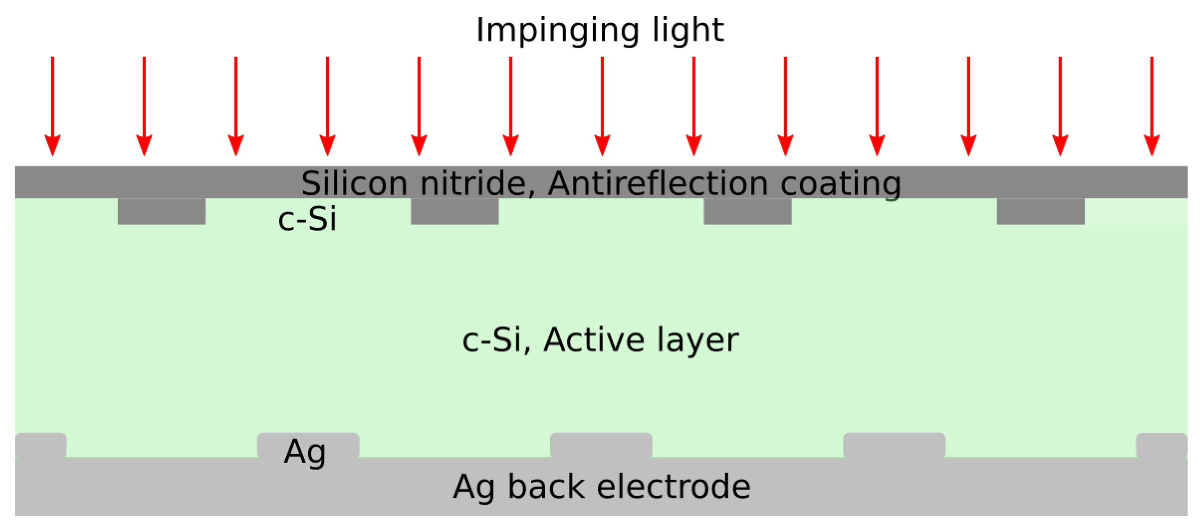
The design of the whole underlying c-Si thin-film solar cell structure is displayed in
Figure 1, and consists of a 400 nm thick crystalline silicon absorbing layer, without doped layers, covered with a 100 nm Si
N
anti-reflection coating on top. The reason for such choice of anti-reflection coating is the appropriate material refractive index for the optimal anti-reflective effect that emerges from a layer with a 100 nm thickness that will completely cover the front grating. The back electrode is a 100 nm Ag layer, where Ag is chosen since the back grating material is also Ag and hence the fabrication process would be easier. It should be mentioned that the top electrode is not included in the simulations, since it has no optical effect on the considered layer stack respectively on the scattering mechanisms in the resulting solar cell topology.
A periodic plasmonic binary Ag back grating with 45 nm tooth height, 175 nm tooth width and a 525 nm periodicity is implemented at the back of the active layer, respective on top of the back electrode. The parameters have been optimized using an evolutionary search heuristics and slightly modified for feasibility reasons. The front grating consists of c-Si, similar to the active layer material, and its physical parameters are chosen based on a direct correlation with the periodic back grating. Our semiperiodic gratings have the same physical parameters as the periodic ones, while just omitting/altering teeth when adding defects.
Furthermore, the excitation is given by a perpendicularly impinging broadband plane wave (covering the spectral range of 350–1100 nm) containing both s- and p-polarization mimicking an AM1.5G solar illumination. The numerical analysis of the overall solar cell is carried out using the simulation platform COMSOL Multiphysics (together with the Wave Optics Module), which is a Finite-Element-Method (FEM) based software. For the optimization procedure, the COMSOL Multiphysics LiveLink for MATLAB has been applied since the optimization code is written in a MATLAB script. This results in slightly longer simulation times compared to the COMSOL Multiphysics optimization package; however, we favor this approach due to the better control over the optimization procedure.
3. Periodic Plasmonic Back Gratings
A common photon management technique relies in adding a periodic plasmonic back grating to the active layer since such grating improves the optical absorption through various scattering channels while simultaneously acting as the back electrode. This back grating may excite several plasmonic modes yielding strong field localizations within the active layer, which improves the optical absorption in the corresponding spectral range. Furthermore, the presence of such artificial roughness in the back of the active layer results in diffuse scattering of the escaped light back to the layer and hence extending the photon path length.
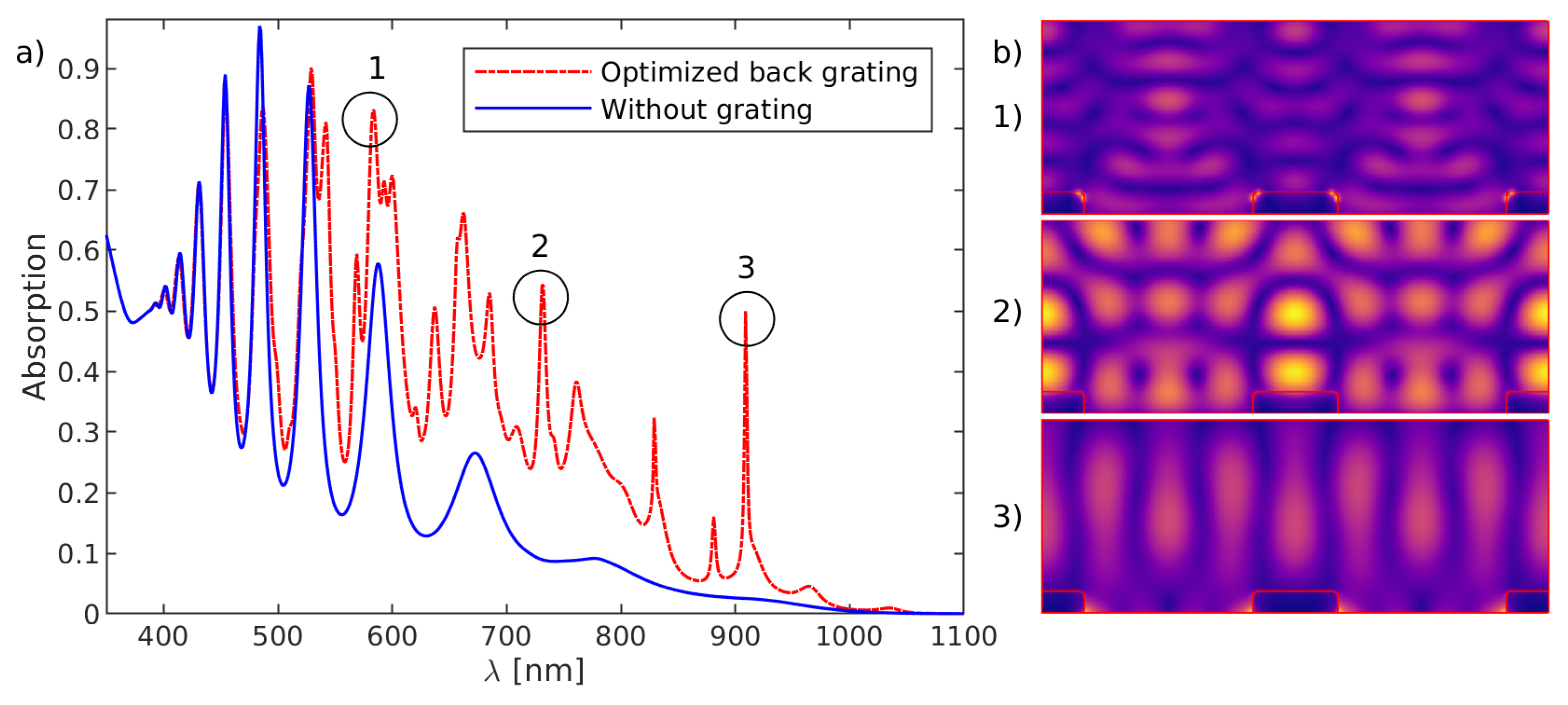
Considering all the mentioned arguments, an Ag rectangular (i.e., binary) back grating is implemented at the back of the structure. The physical parameters of the grating, namely the grating period, tooth height and tooth width determine its functionality regarding to the number and spectral positions of the modes which are excited. Considering the intended ultra-broadband performance of the solar cell, where a spectral range between 350–1100 nm of an AM1.5G illumination spectrum is addressed, the mentioned parameters cannot be designed for only a narrow spectral range. In this regard, the grating parameters (such as grating tooth height, width and periodicity) were subjected to optimization where the spectrally integrated optical absorption acted as the quality respective the fitness function. The optimization was terminated after about 800 iterations when the final population reached a certain level of quality and afterwards the best performing structure was analyzed. The optimized structure absorbs of the total illuminated power, which is higher compared to the same structure without periodic back grating.
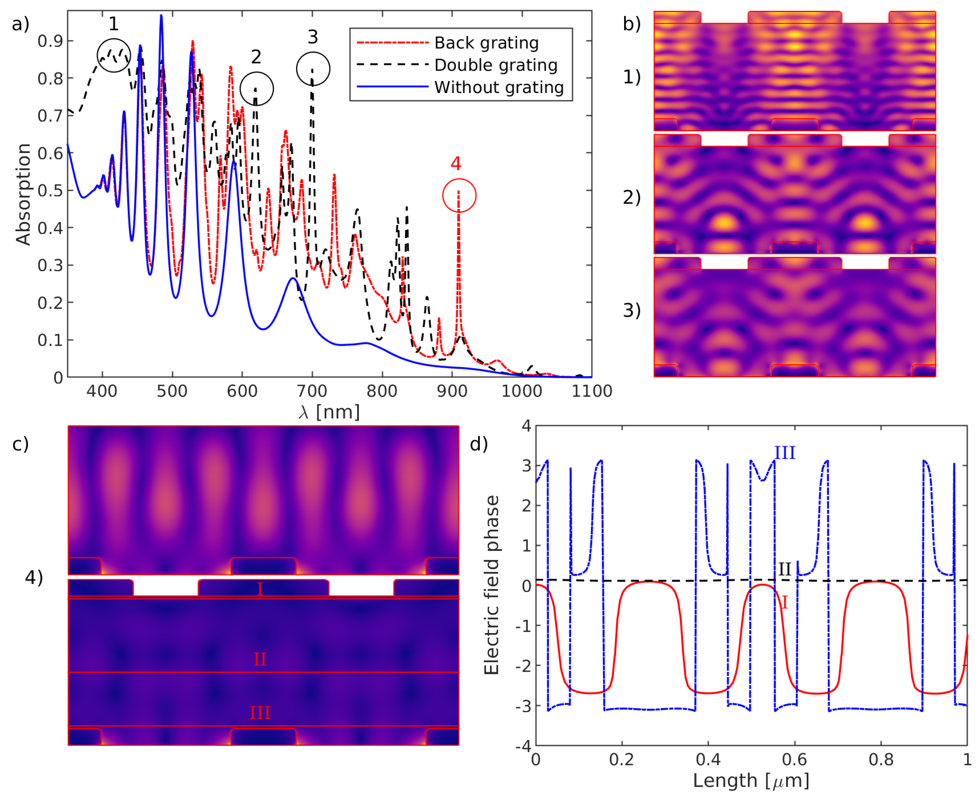
The simulated spectral response of the active layer’s optical absorption in the structure with optimized periodic Ag back grating compared to a similar structure without any back grating is depicted in
Figure 2a. It can be seen that various new peaks emerged in the absorption spectra due to the presence of the back grating. To study the reason behind each peak, the electric field distribution at the corresponding wavelengths are investigated and illustrated in
Figure 2b, where the first peak is associated to a plasmonic mode that is excited around each tooth. The second and third peaks refer to similar strong field localizations, which also resulted in improved optical absorption. However, it should be mentioned that all the peaks appear as quite narrowband.
4. Periodic Double Gratings
Adding a front grating will further improve the solar cell performance owing to various mechanisms. The front grating can be regarded as a controllable surface roughness, which, through deviating the incident light direction, extends the photon path within the active layer. Surface roughness by diffusely transmitting the incoming light into the active layer at angles smaller than those of total internal reflection trap the light inside the active layer, when such back and forth scattering at interfaces further extends the photon path four or five times within the active layer [
20].
Despite having a 100 nm
anti-reflection coating on top of the active layer, a considerable amount of the illuminated power is still reflected and hence lost without entering the active layer. Another aspect of adding a front grating to the active layer is to further reduce such reflection as the front grating creates an intermediate layer with refractive index amid the anti-reflection coating and the active layer [
21]. This results in the formation of a graded refractive index layer stack which consequently improves the incoupling performance [
22,
23,
24,
25,
26].
Additionally, each tooth acts as an elementary light source that injects diffused light into the active layer while various modes and mode groups are excited within the active layer. Constructive interferences among the excited modes in the front and back gratings would result in strong field localizations (i.e., hot spots) which may directly correspond to strong peaks in the optical absorption spectra. However, destructive interferences are also possible and hence a careful design of front grating parameters along with its phase relative to the back grating is needed to minimize the effect of such destructive interferences.
The first important parameter in designing a front grating is the material. Plasmonic materials cannot be positioned on top of the active layer due to their high absorption and correspondingly high loss. Since creating a new interface between the active layer and the front grating would result in higher reflection, in this work, the front grating material is chosen to be c-Si, which corresponds to the active layer material. Such design would also result in easier fabrication. As the main criteria for the front grating parameters are their direct correlation with the back grating, the front grating’s physical parameters, namely tooth height and width are considered to be related to the corresponding optimized values of the back grating and hence are chosen accordingly. The front grating parameters are either the same, double or half of the back grating parameters. The front grating phase relative to the back grating (i.e., the grating offset) is a critical parameter that determines the front-back gratings coupling. Two cases of in-phase and out-of-phase front gratings are considered where in-phase means that each front grating tooth is positioned at the exact same position of the back grating tooth, while out-of-phase refers to a front grating tooth that is positioned in between two back grating teeth.
The percentage of spectrally integrated absorbed power along with the reflected power relative to the total illuminated power for the mentioned double grating structures are presented in
Table 1, which shows that the best performing structure (45 nm tooth height, 350 nm tooth width and in-phase with the back grating) improves the spectrally integrated optical absorption by
compared to the case with only a back grating. The spectral response of the active layer’s optical absorption for the mentioned structure together with the structure with only a back grating and without any grating are depicted in
Figure 3a. One interesting feature of this graph is the prominent enhancement of the optical absorption in the spectral range 350–450 nm which is mainly due to the reduced reflection. In the
Figure 3b-1, the electric field distribution at a typical wavelength in this range is illustrated which clearly shows strong light injection into the active layer through the front grating. Studying the electric field distributions at other peaks in the optical absorption validates the fact that strong field localizations happen as a consequence of front grating presence (cf.
Figure 3b-2,3).
It should also be mentioned that in some cases the absorption is reduced which is mainly due to destructive interference between the front and back gating. An example of such destructive interference emerges at 910 nm as indicated in
Figure 3a. The electric field distribution at the corresponding wavelength for the structures with a periodic double grating and only a periodic back grating is shown in
Figure 3c together with the phase of the electric field within the active layer (cf.
Figure 3d). The destructive interference between the back and front gratings resulted in a weak electric field distribution throughout the active layer and consequently in poor absorption.
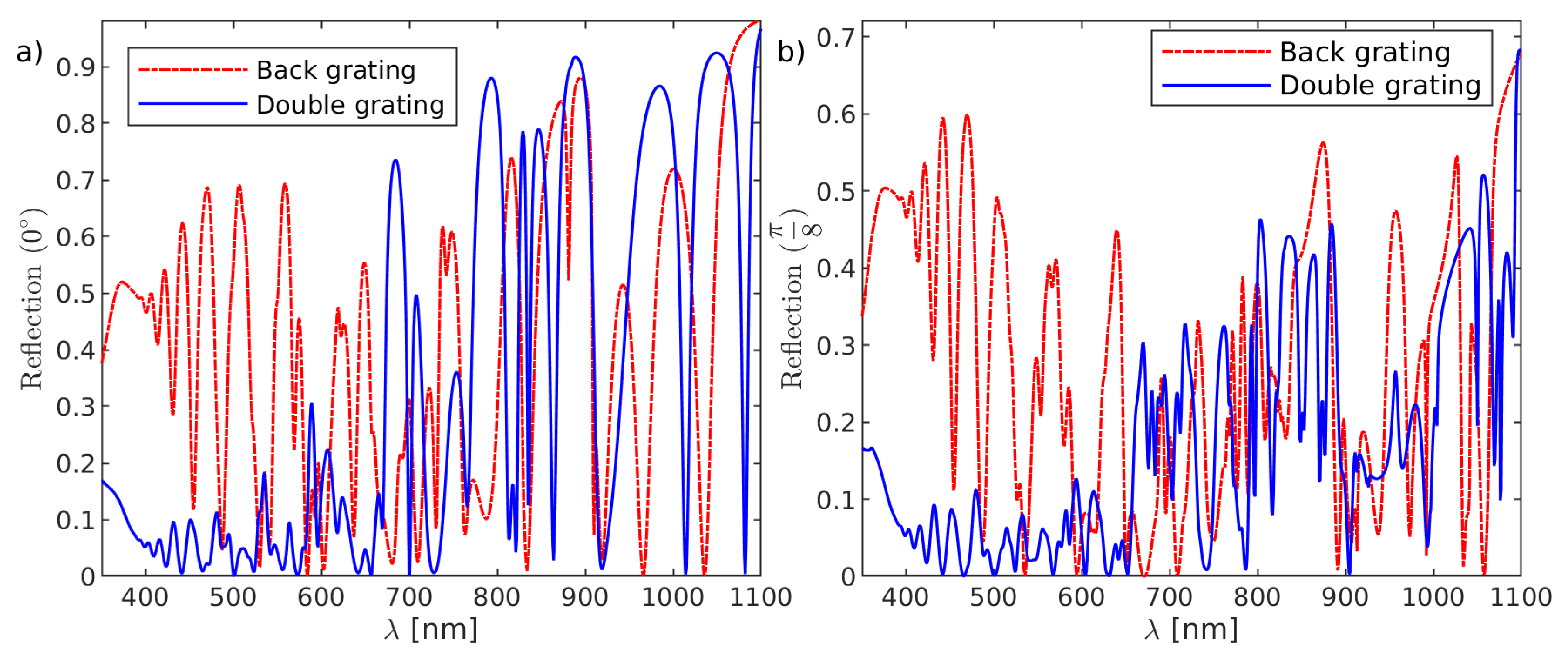
As discussed and already shown in
Table 1, the presence of a front grating substantially reduces reflection. This reduction is even more pronounced at oblique illuminations, which is advantageous as reflection is a major issue in the solar cell’s performance at these oblique incidences. Another advantage of the front grating as the anti-reflection coating is its inherent tendency toward omnidirectionality. In
Figure 4, the spectral response of the reflected power for an illumination angle of 0 and
are plotted in comparison to the structure with only a back grating, where it can be seen that the presence of the front grating reduced the reflection at both illumination angles in particular in the short wavelength regime where c-Si is a good absorber.
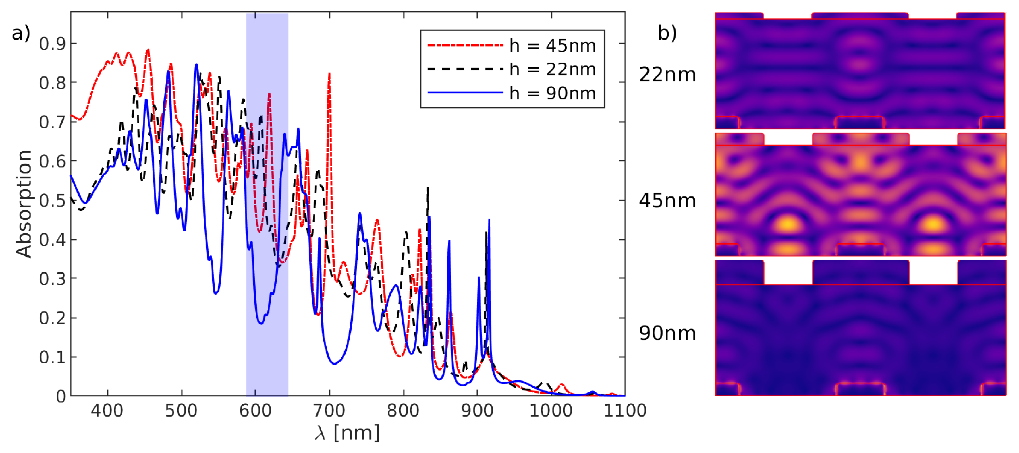
The front grating’s tooth height is a deterministic parameter which affects the performance of the front grating as both, a light coupler and an anti-reflection coating. In order to reduce backscattering, the grating tooth should not be too high and hence values around 90 nm, 45 nm and 22 nm are investigated aiming at an improved light coupling to the active layer. As expected, the 90 nm tooth height doesn’t show an improvement in the optical absorption since it backscatters a huge fraction of light and shows a
higher reflection compared to the structure with only a back grating. In addition, a 22 nm tooth height is not capable of exciting various modes and conclusively a 45 nm tooth height which is identical to the back grating’s teeth shows both, better anti-reflection capabilities and strong mode excitations within the grating (cf.
Figure 5).
The front grating’s tooth width should also be chosen with care in order to achieve a strong light coupling to the active layer. Correspondingly, values such as 350 nm, 175 nm and 87 nm for the tooth widths are simulated and the spectral response of the active layer’s optical absorption along with the reflected power are illustrated in
Figure 6. We can now deduce that a 350 nm width has the lowest reflection and hence results in better optical absorption. In order to validate that the improvement in the optical absorption is not simply the result of a slightly increased active material volume due to the presence of the front grating, the volume density of the optical absorption is calculated for all structures showing the same improvement as the optical absorption.
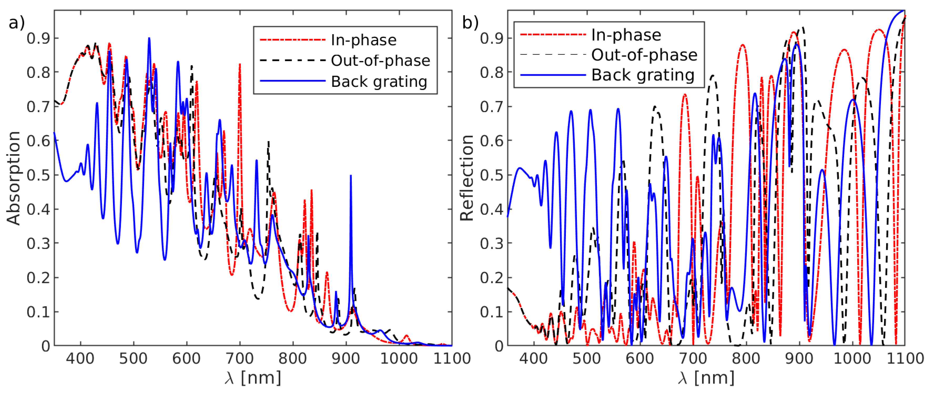
For an optimal periodic double grating design, the effective coupling between front and back gratings is vital. The relative phase of the front grating in regard to the back grating is the determining parameter that should be carefully chosen according to a predominate number of constructive interferences in the desired spectral range compared to the number of destructive interferences. Two cases of in-phase and out-of-phase front gratings concerning possible front-back grating coupling are studied and the results are depicted in the
Figure 7. The spectrally integrated optical absorption in the case of the periodic in-phase double grating is about
higher than for the out-of-phase case, which is due to a better front-back gratings coupling.
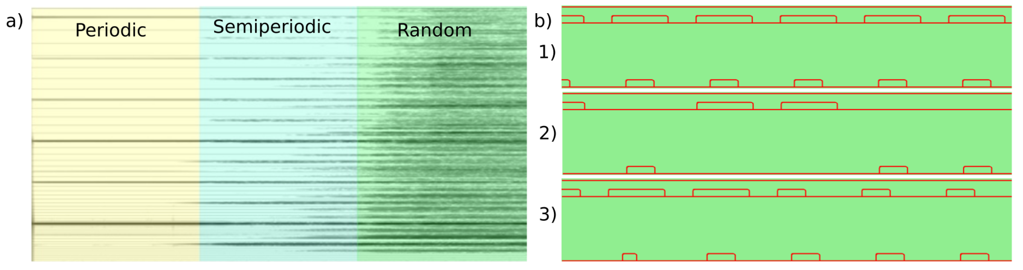
5. Semiperiodicity
Semiperiodicity or aperiodicity is a concept basically meaning order without periodicity, and became a hot topic in various fields such as e.g., mathematics, physics, biology and economy [
27]. Traditionally, systems are divided into two groups of periodic and non-periodic structures and are treated accordingly. However, there is a rich field in between that is associated with semiperiodicity and can be categorized based on their degree of order respective to their underlying spatial correlations. Semiperiodic structures have various potential applications especially in broadband optical systems [
17,
28], since they lie somewhere between full periodicity and randomness and therefore can provide a trade-off between the expected performances of these two characteristic topologies. Fully periodic structures consist of repeated building blocks respective unit cells in space and hence display long range order which corresponds to the excitation of strong but narrowband modes. In comparison, random structures are capable of simultaneously exciting several modes and mode groups, which are quite broadband however weak. Semiperiodic structures have some degrees of order and although each realization will not behave exactly as the other, there would be some correlations amongst these realizations and consequently such structures can sustain modes that are both not as narrow as in fully periodic structures and not as weak as in random structures, and hence provide a nice compromise for broadband optical applications.
Designing semiperiodic structures is nonetheless quite challenging since there is no explicit way of capturing semiperiodicity in a structure and accordingly there is some research regarding the proper definition of semiperiodicity [
19,
29,
30]. The approach that is used here is adding defects to a fully periodic grating in order to “move” toward randomness. Adding defects means omitting teeth in the fully periodic grating. The idea is schematically illustrated in
Figure 8, where the first structure in
Figure 8b is fully periodic; in the second structure, some defects are added based on an already existing mathematical semiperiodic sequence, namely the Thue–Morse sequence [
31]. The Thue–Morse sequence is mapped in parallel onto both periodic gratings with commonsurable lengths, where the zeros of the Thue–Morse sequence are labeling the locations of the missing teeth. The defects are added to both, front and back grating, where the back grating is mapped based on the Thue–Morse sequence while the front grating is processed according to the bitwise negation of the Thue–Morse sequence (i.e., each bit has the opposite value of the same bit in the binary representation of the sequence) [
17]. The third structure is our fully optimized semiperiodic double-grating structure resulted from numerical structural optimization where both front and back gratings were subjected to optimization.
6. Semiperiodic Double Gratings
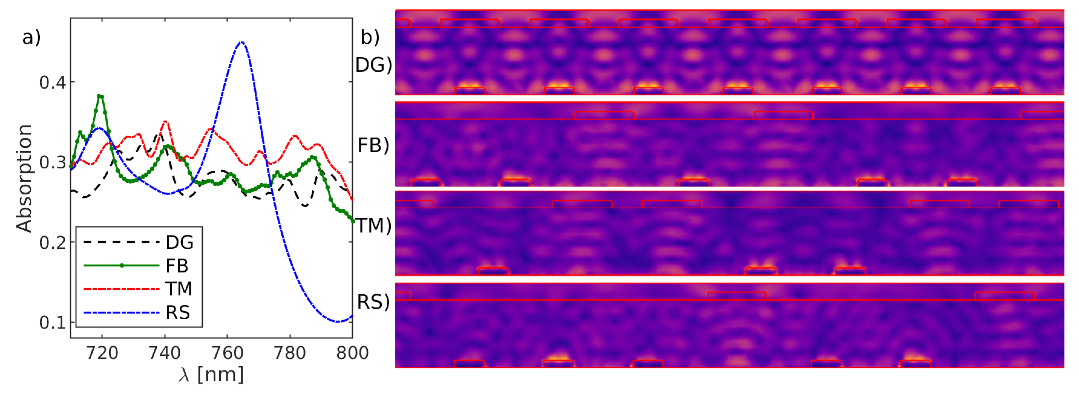
A well-designed semiperiodicity would allow the capturing of the solar illumination in its broad spectral range. This idea is first tested through defining semiperiodicity based on corresponding mathematical sequences, such as Thue–Morse, Fibonacci and Rudin–Shapiro sequences [
17,
31]. The results in terms of the spectral response of the active layer’s optical absorptions are depicted in
Figure 9a for a wavelength range of 700–800 nm. Here, a narrow but strong peak in the periodic double grating is transformed into a broad though weaker absorption which applies for all semiperiodic sequences. Through analyzing the electric field distribution at the corresponding operating wavelength (cf.
Figure 9b), it can be conferred that, in all semiperiodic cases, the electric field is dispersed through the whole active layer instead of being localized in some hot spots, indicating that the entire active material volume is contributing uniformly to the optical absorption.
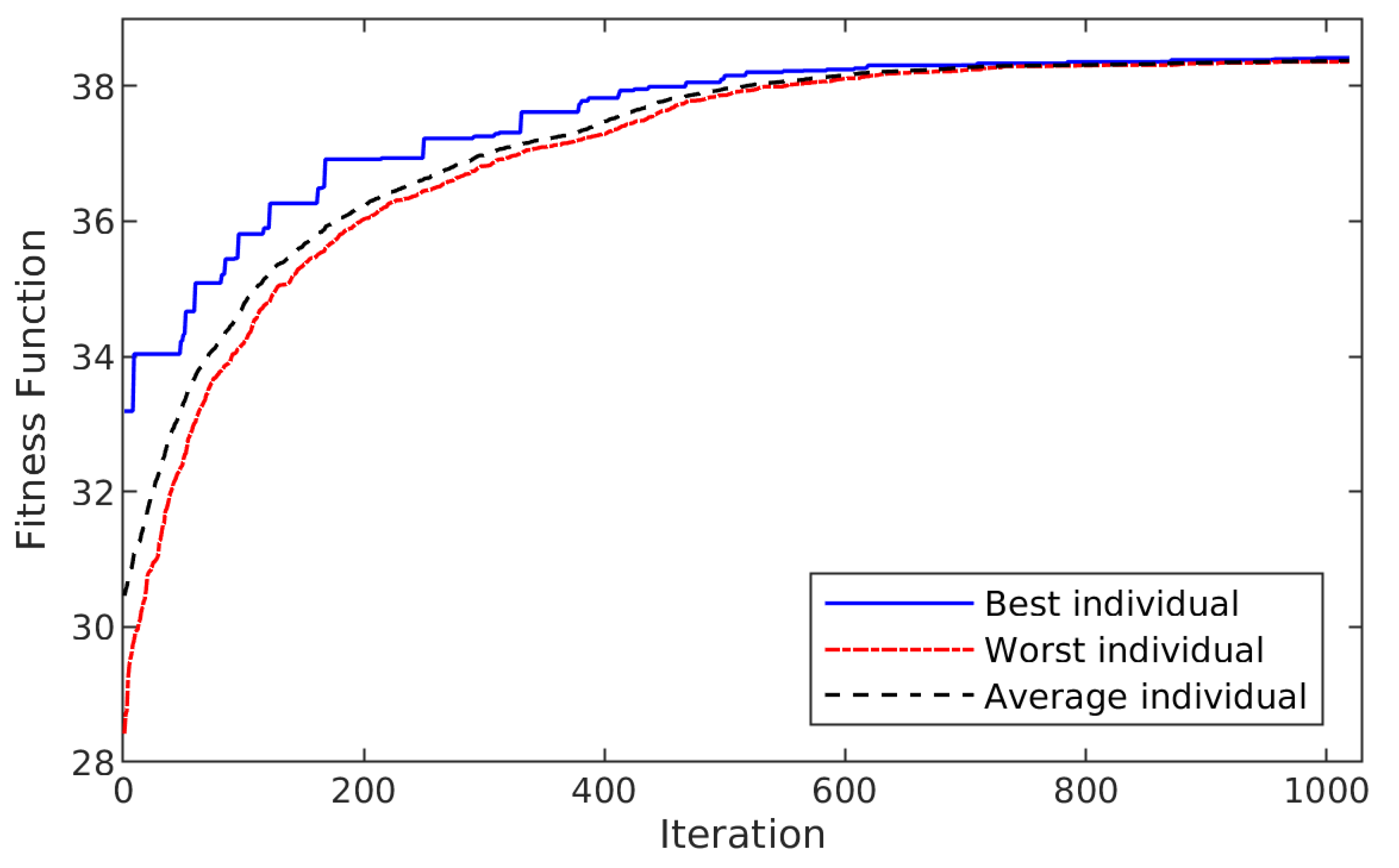
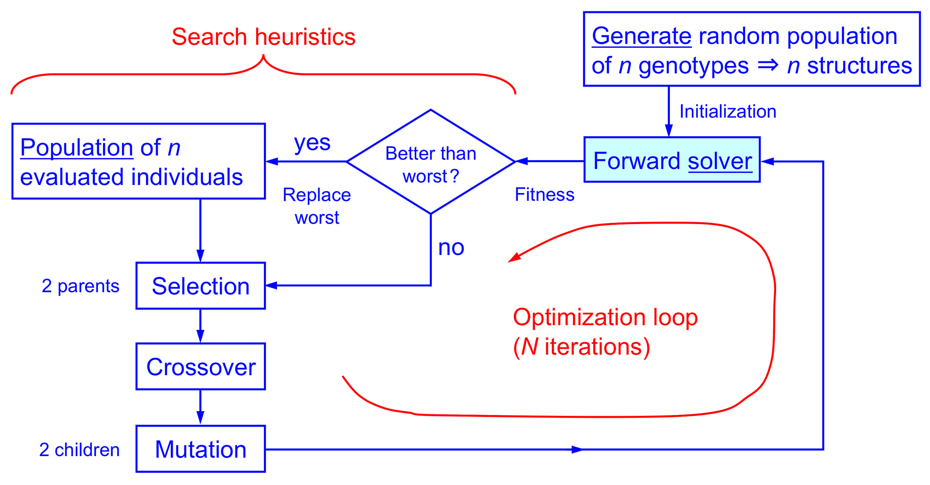
Defining semiperiodicity based on mathematical sequences, despite showing the advantages of such approach, is not enough to reach an optimal design for an ultra-broadband solar cell. To reach such design, a breeder evolutionary algorithm is used to create fully semiperiodic double grating purely based on this global optimization scheme. The details of the optimization procedure are provided in
Appendix A. In this approach, the position of each defect as well as each tooth width (tooth widths have either half or the same value as in the periodic design) are determined by the optimization, considering a maximal spectrally integrated optical absorption as the optimization criterion. In addition, no direct correlation between back and front grating is taken into account so the geometry would totally evolve by itself. The optimization procedure was terminated after about 1020 iterations when the best performing structures within the final population achieved a good approximation to the given specifications. The fitness functions of best, worst and average individuals in the population for each iteration step are illustrated in
Figure 10. This evolution clearly shows the wide range of possibilities that were explored by this global optimization procedure. The fitness of each structure is given by the percentage of spectrally integrated optical absorption relative to the total illuminated power.
The best performing of the optimized semiperiodic double gratings achieved a promising spectrally integrated optical absorption that is
higher compared to the same structure without any grating. The quantitative values for the percentage of spectrally integrated absorbed power relative to the total illuminated power for all semiperiodic double grating designs are provided in
Table 2, which states that the optimized semiperiodic double grating provides the highest spectrally integrated optical absorption. To comprehend the underlying mechanisms that contribute to the performance of the optimized structure, the simulated spectral response of the active layer’s optical absorption is displayed in
Figure 11 in comparison to the corresponding spectra of the semiperiodic structures based on the mathematical sequences as well as for the fully periodic double grating. The comparison between the spectral responses of the active layer’s optical absorption shows that, although the optimized structure doesn’t show strong peaks, it maintains a nice compromise between peak strength and peak bandwidth, which is advantageous in such broadband application.
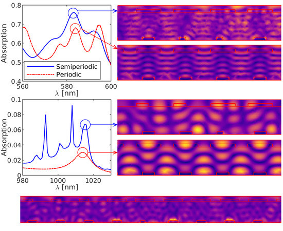
There are various interesting features when comparing the optimized semiperiodic double grating structure’s optical absorption with the performance of the fully periodic one, which are highlighted in
Figure 11b, together with the corresponding electric field distributions that are analyzed and depicted in
Figure 12. The first characteristic feature emerges around 583 nm where the semiperiodicity resulted in an even stronger absorption peak compared to the fully periodic one. The electric field distributions of both double grating structures show that the semiperiodicity in the front grating resulted in better and more diffused light coupling to the active layer and consequently the optical absorption is increased (cf.
Figure 12a). The same analysis at 764 nm depicts that in this case the electric field is more dispersed through the active layer which corresponded to the transformation of a strong peak in the periodic case into a broad absorption band (cf.
Figure 12b). At 1014 nm, the effective break of periodicity in the underlying structure dispersed the light even better throughout the active layer where in addition a stronger coupling among the back grating teeth has occurred yielding stronger optical absorption (cf.
Figure 12c).
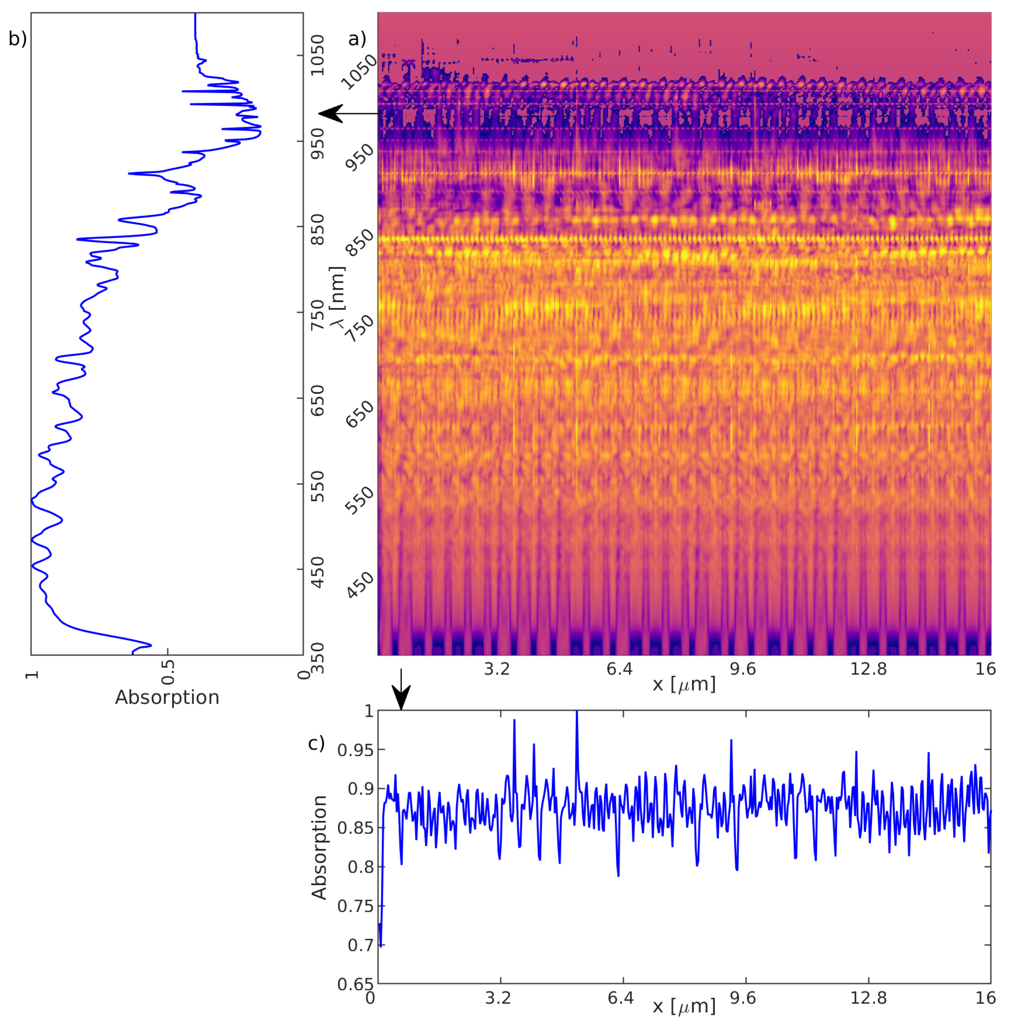
To be able to reliably deduce that the optimized semiperiodic double grating structure achieved a dispersed optical absorption throughout the whole active layer, a comprehensive display of the active layer’s overall optical absorption has been generated in the form of a two-dimensional (2D) spatio-spectral (normalized) absorption density map that is depicted in
Figure 13a. This map is complemented by two insets showing the spatial integration of the map (i.e., the frequency response of the overall optical absorption) in
Figure 13b as well as the spectral integration of the map (i.e., the spatial distribution of the overall absorption) in
Figure 13c. Please note that the full 2D integration of the absorption density map refers to the fitness value that has been maximized within optimization. Given this sort of holistic display of the optimized solar cell’s performance allows now to verify that the achieved semiperiodicity renders the resulting absorption to be distributed in the best possible way i.e., showing the intended broadband features in the spectral response together with a virtually uniform exploitation of the active layer volume.
7. Conclusions
In this work, the concept of semiperiodicity as an apt solution to broadband optical applications is introduced and used to improve spectral response of the optical absorption in c-Si thin-film solar cells. It is shown that using a well-defined semiperiodic grating structure can result in an effective exploitation of the active material in the spatial as well as in the spectral domain.
An optimized periodic plasmonic back grating as a first example of a photon management technique is implemented in the active layer taking the spectrally integrated optical absorption as the figure of merit. Results show that the designed grating improves the solar cell’s performance up to , compared to a bare solar cell due to the excitation of several well-defined modes within the active layer.
As the next step, a periodic c-Si front grating is added to the discussed topology, which acts as an omnidirectional anti-reflection coating as well as a light coupler to the active layer and hence the active layer’s optical absorption is further improved. It is shown that physical parameters of the underlying front grating are key in order to establish a constructive coupling between the two gratings. However, the resulted spectral response of active layer’s optical absorption shows mainly strong but narrowband peaks, which leaves considerable part of the solar spectrum unused.
Applying now the concept of semiperiodicity to the design of semiperiodic double gratings, a more efficient spectral response of the active layer optical absorption is achieved, since the semiperiodic double grating is capable of creating broad optical absorption bands. The main reason lies in the broad dispersion of the electric field throughout the whole active layer instead of having some localized hot spots. Our approach towards defining semiperiodicity is adding defects in the sense of missing teeth into the periodic double grating, which, at the first stage, were introduced through mathematical semiperiodic sequences. To accomplish an optimal design, the semiperiodic sequence is realized through a numerical structural optimization ascertaining the best optical performance for the underlying solar cell structure. The proposed structure enhanced the spectrally integrated optical absorption up to compared to a bare reference structure without gratings. Our design approach underpins the fact, that the performance of the best semiperiodic double grating topology is strongly related to a virtually uniform spatio-spectral exploitation of the solar cell’s active material stack. This is not very surprising; however, it aims at a more holistic view to broadband photonic design, namely at spatio-spectral performance measures with complex interdepenencies that are only manageable in the framework of numerical structural optimization.


