Nanoscale Mechanical and Mechanically-Induced Electrical Properties of Silicon Nanowires

Abstract
:1. Introduction
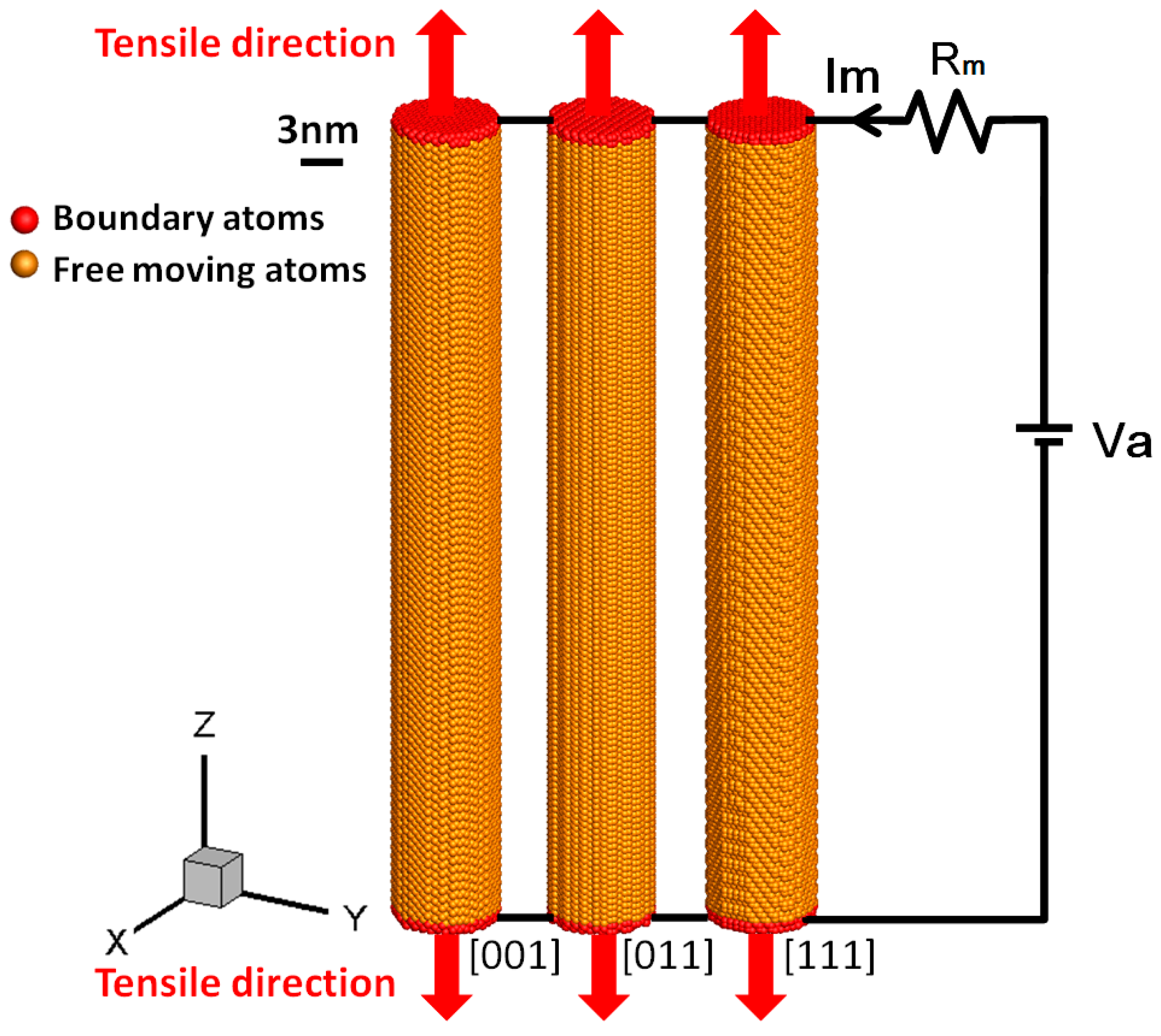
2. Methodology
3. Results and Discussion
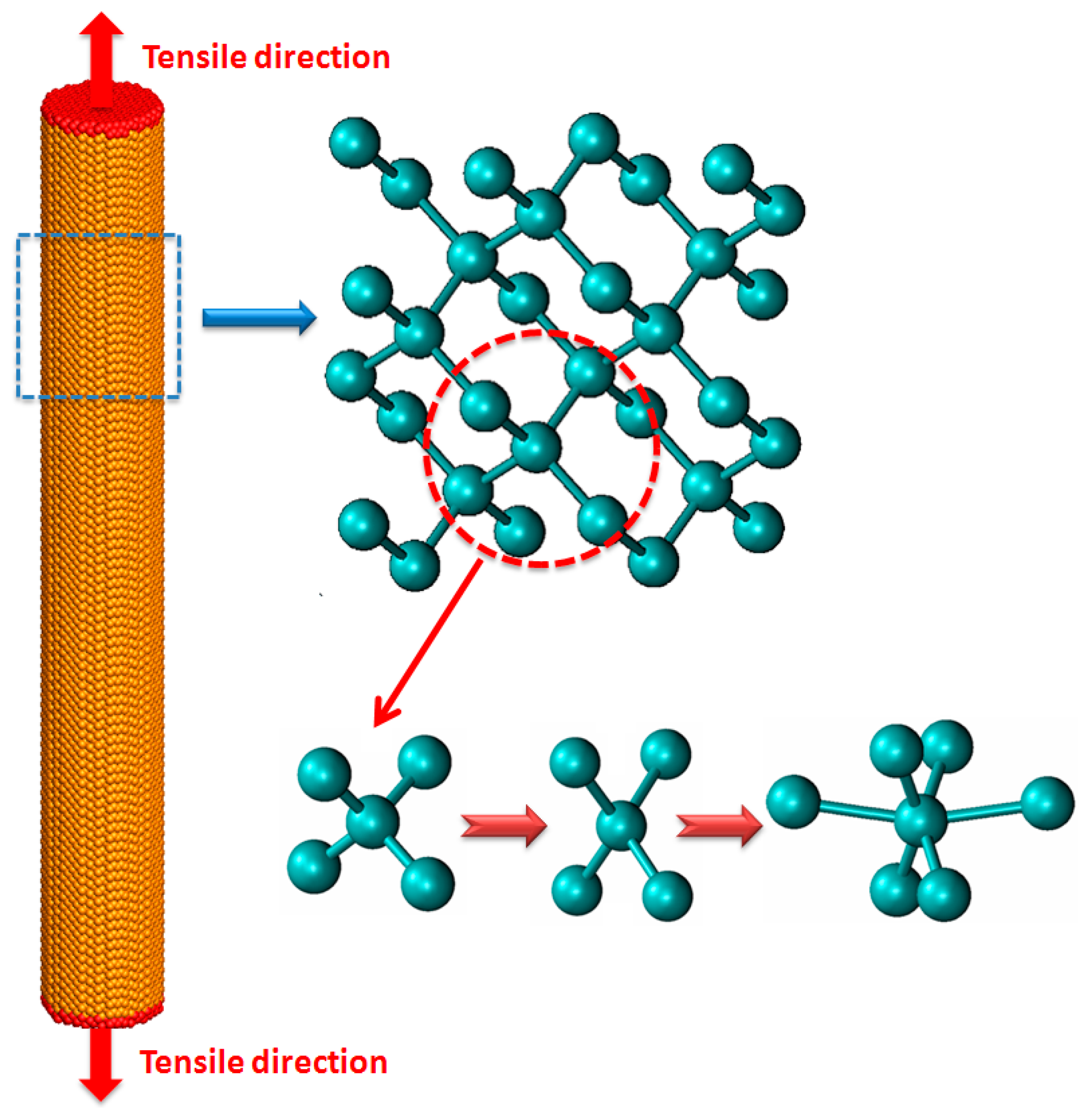
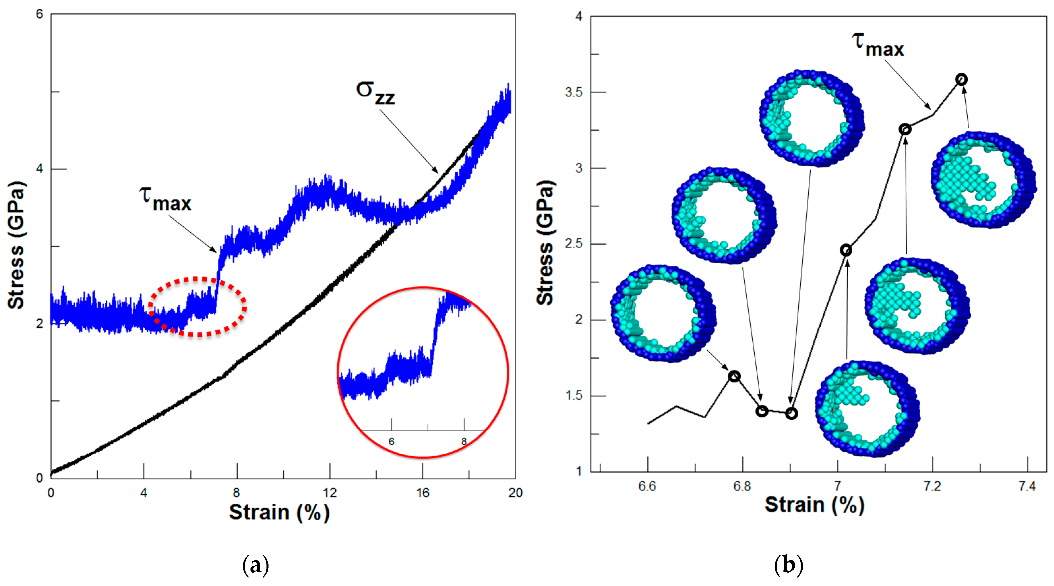
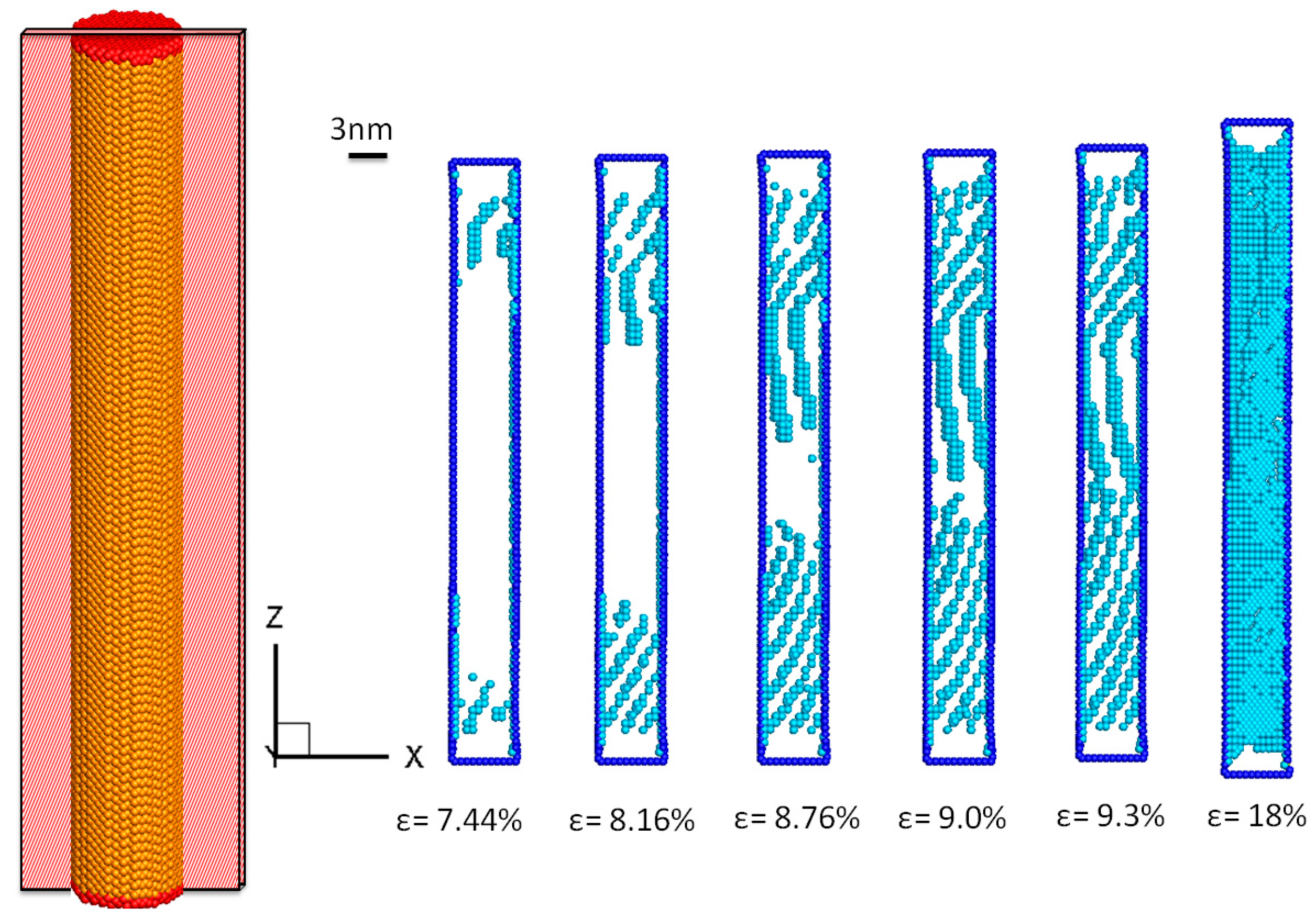
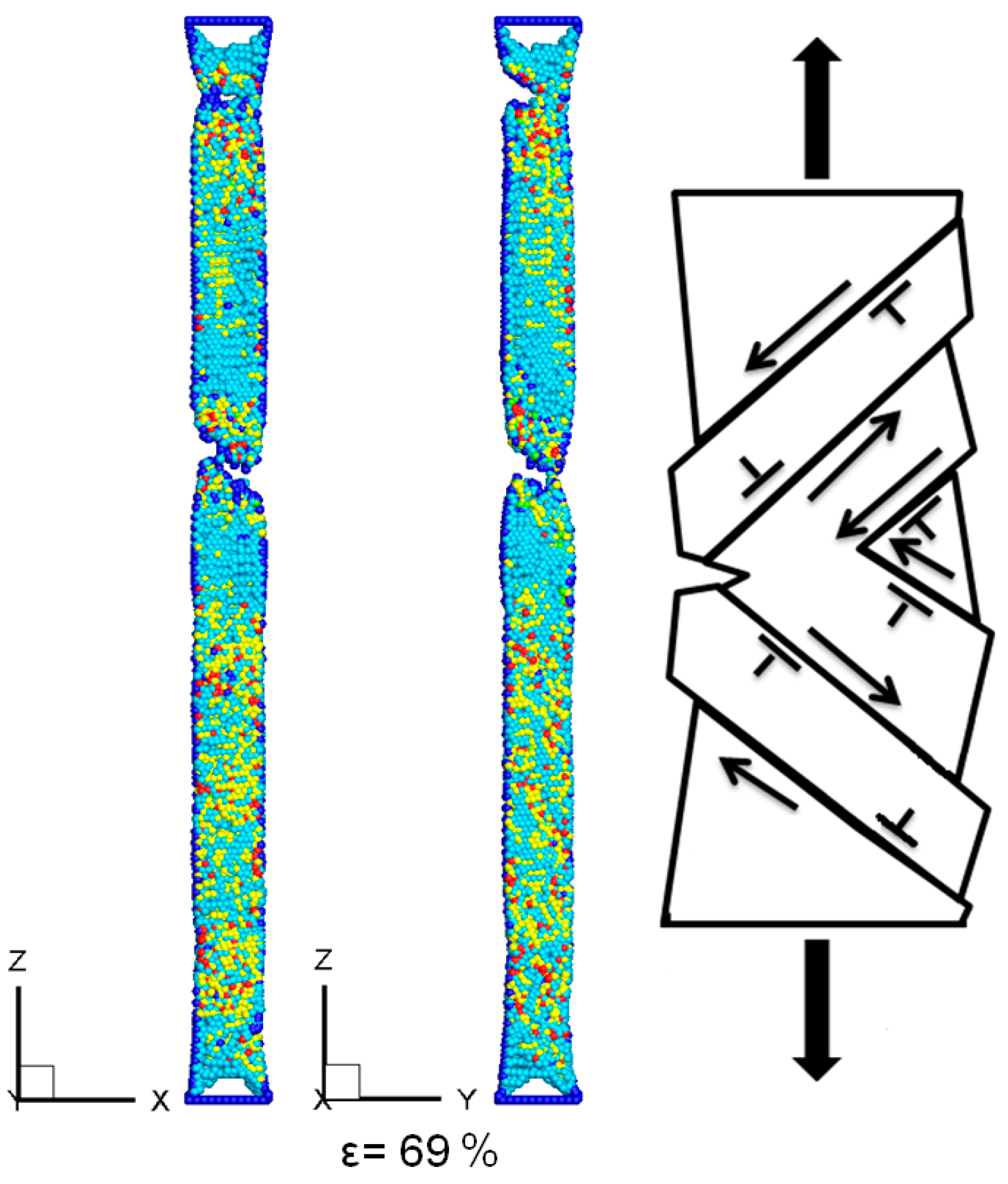
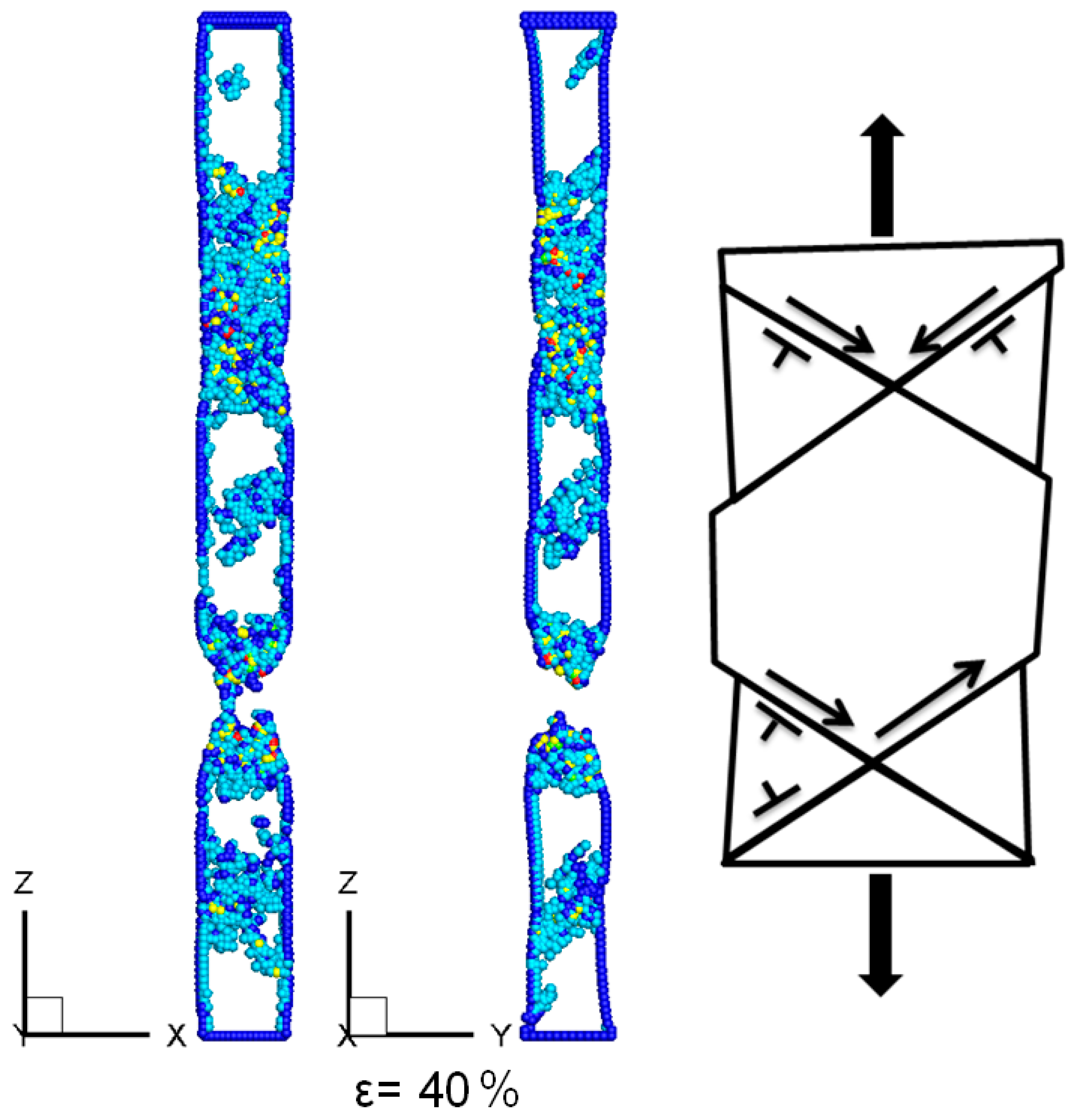
3.1. Mechanical Behaviors of Nanostructured Si Nano Wire
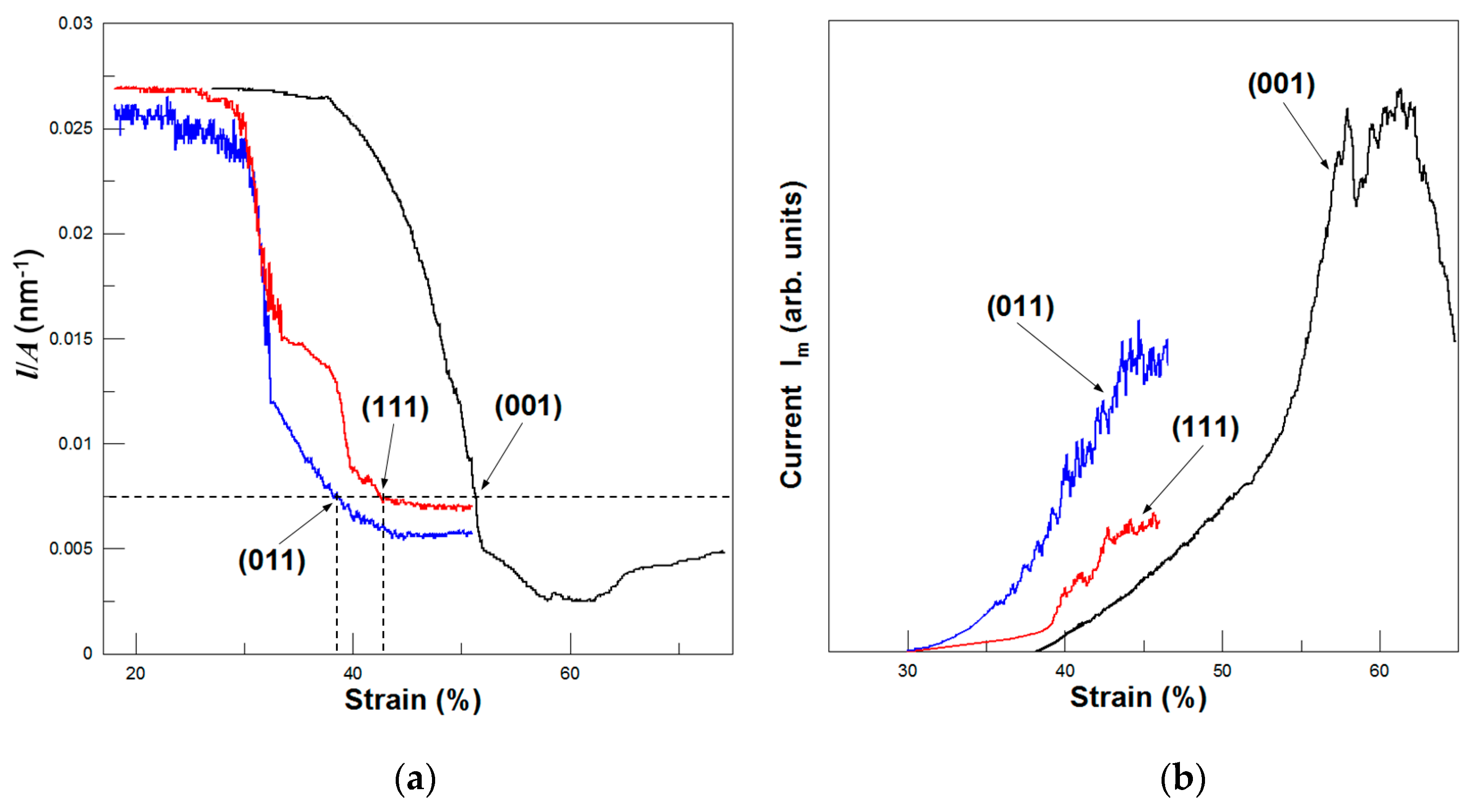
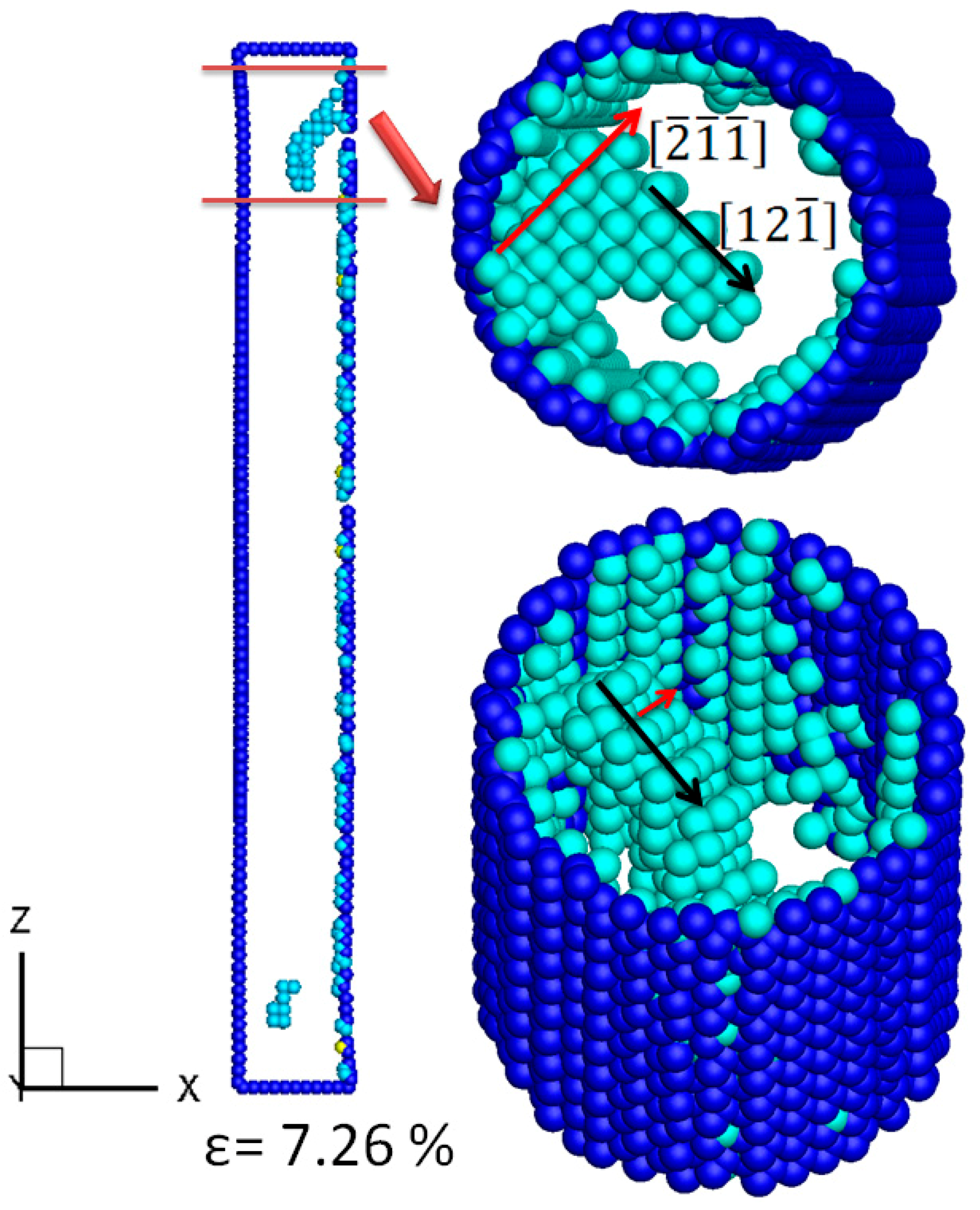
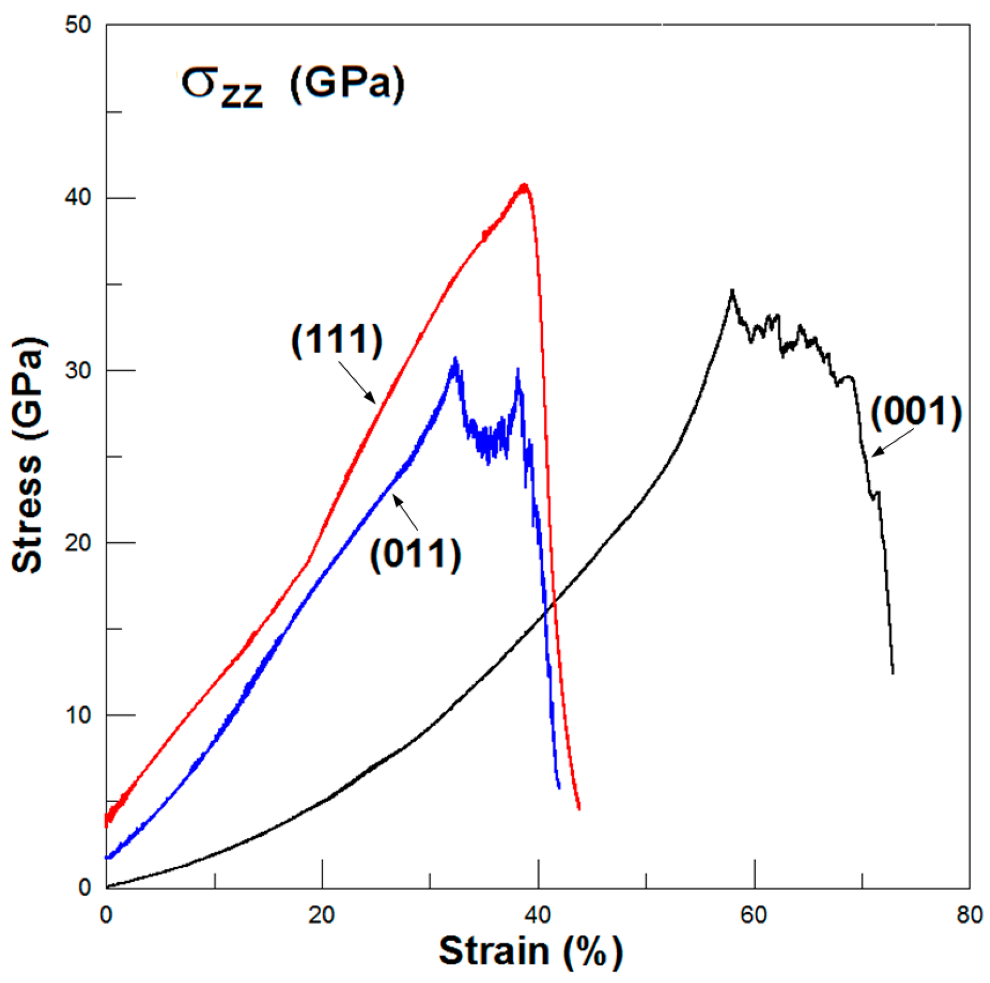
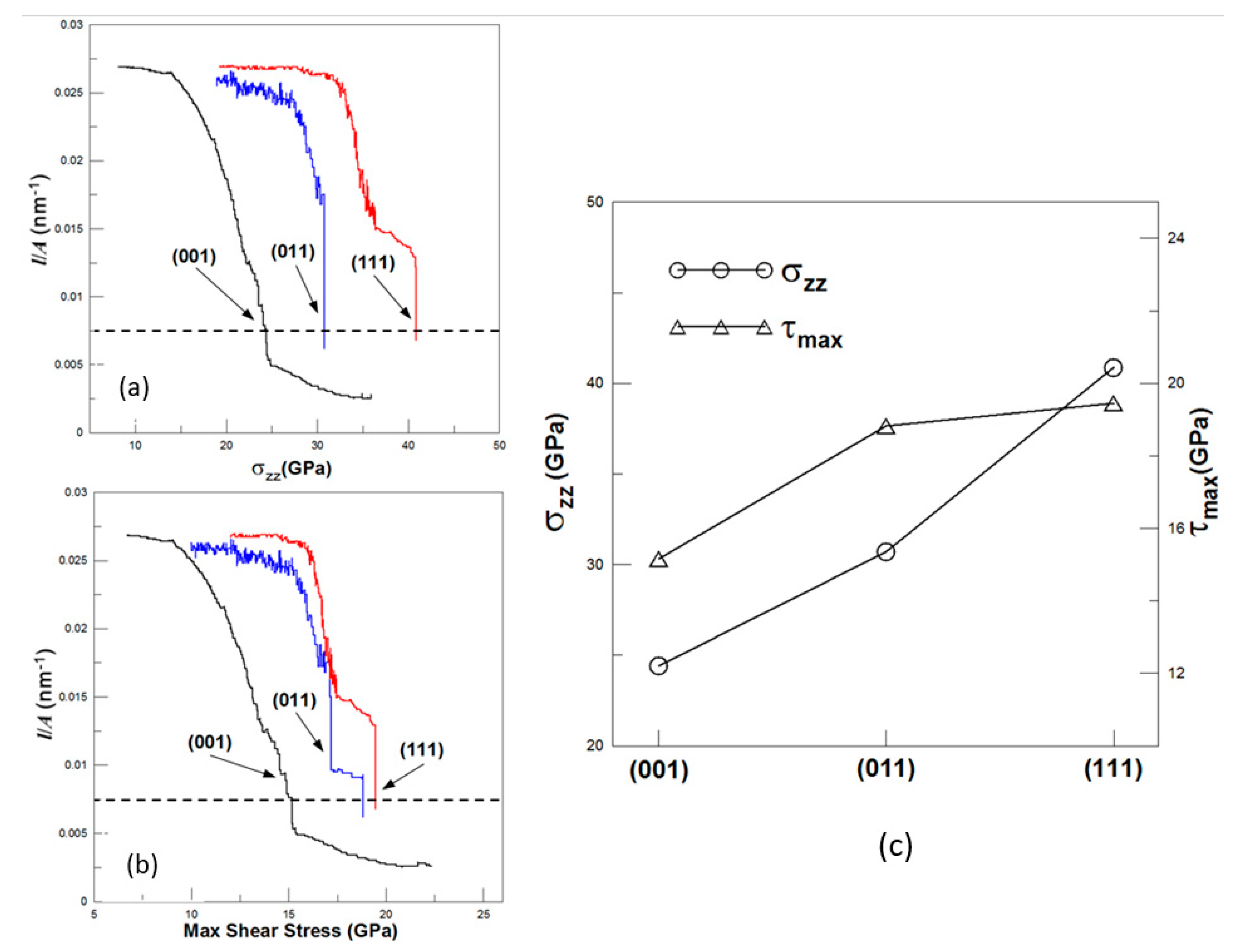
3.2. Effects of Surface Orientation
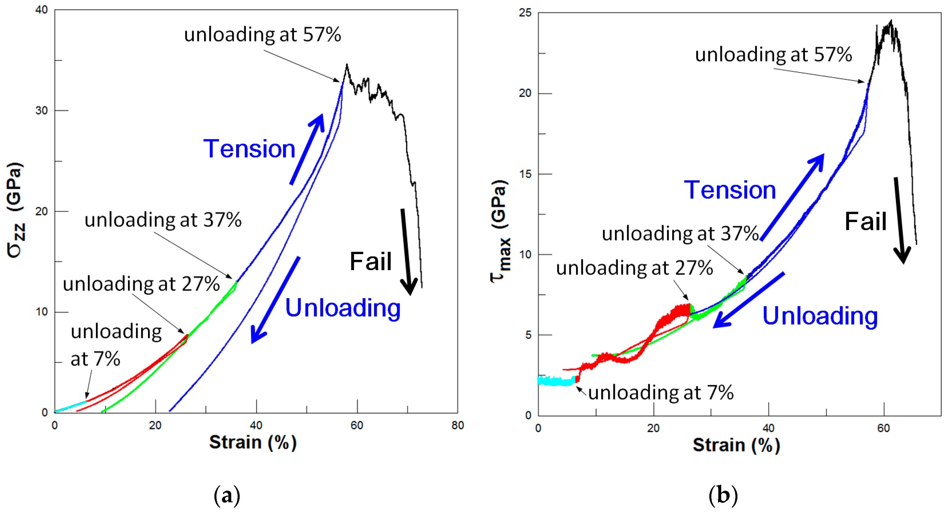
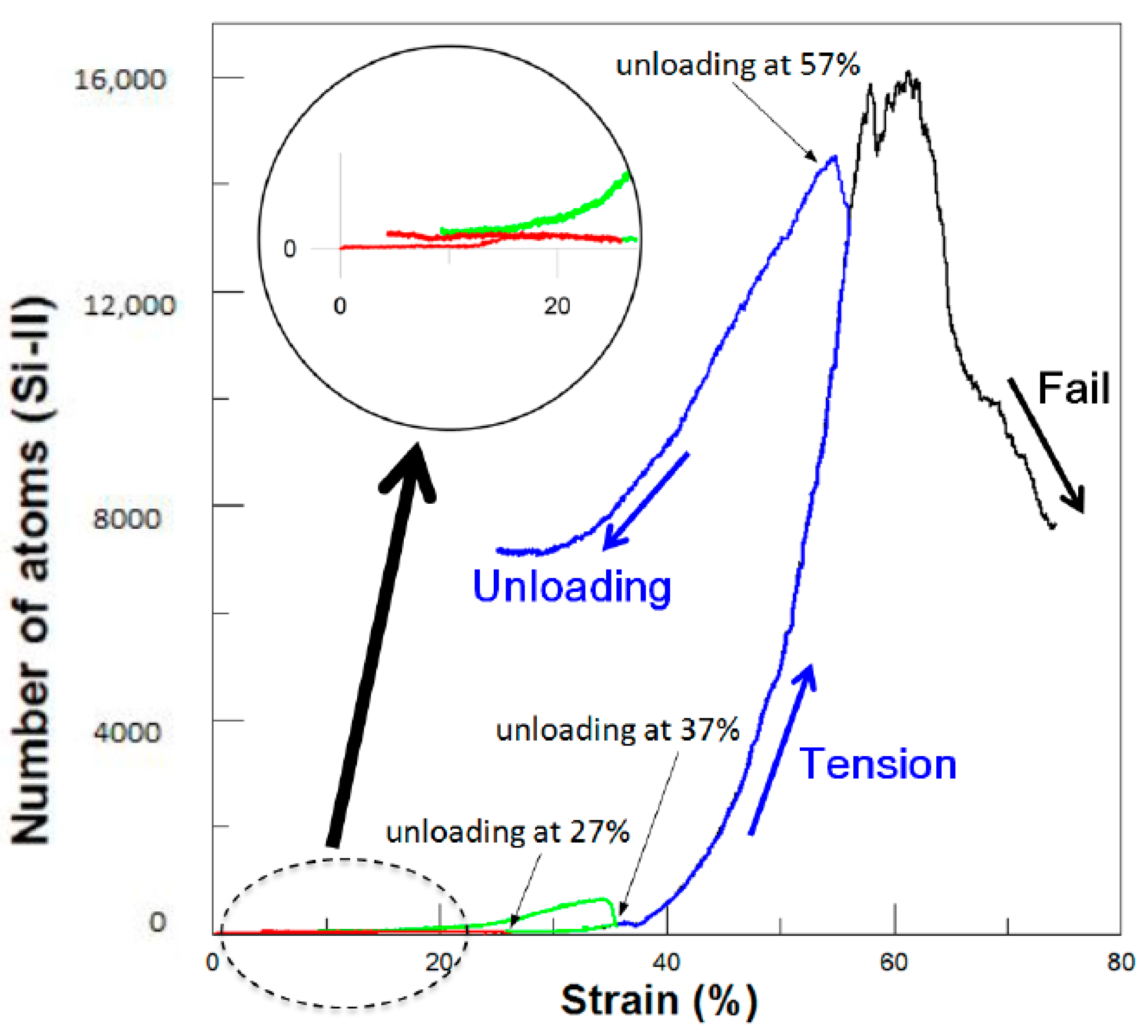
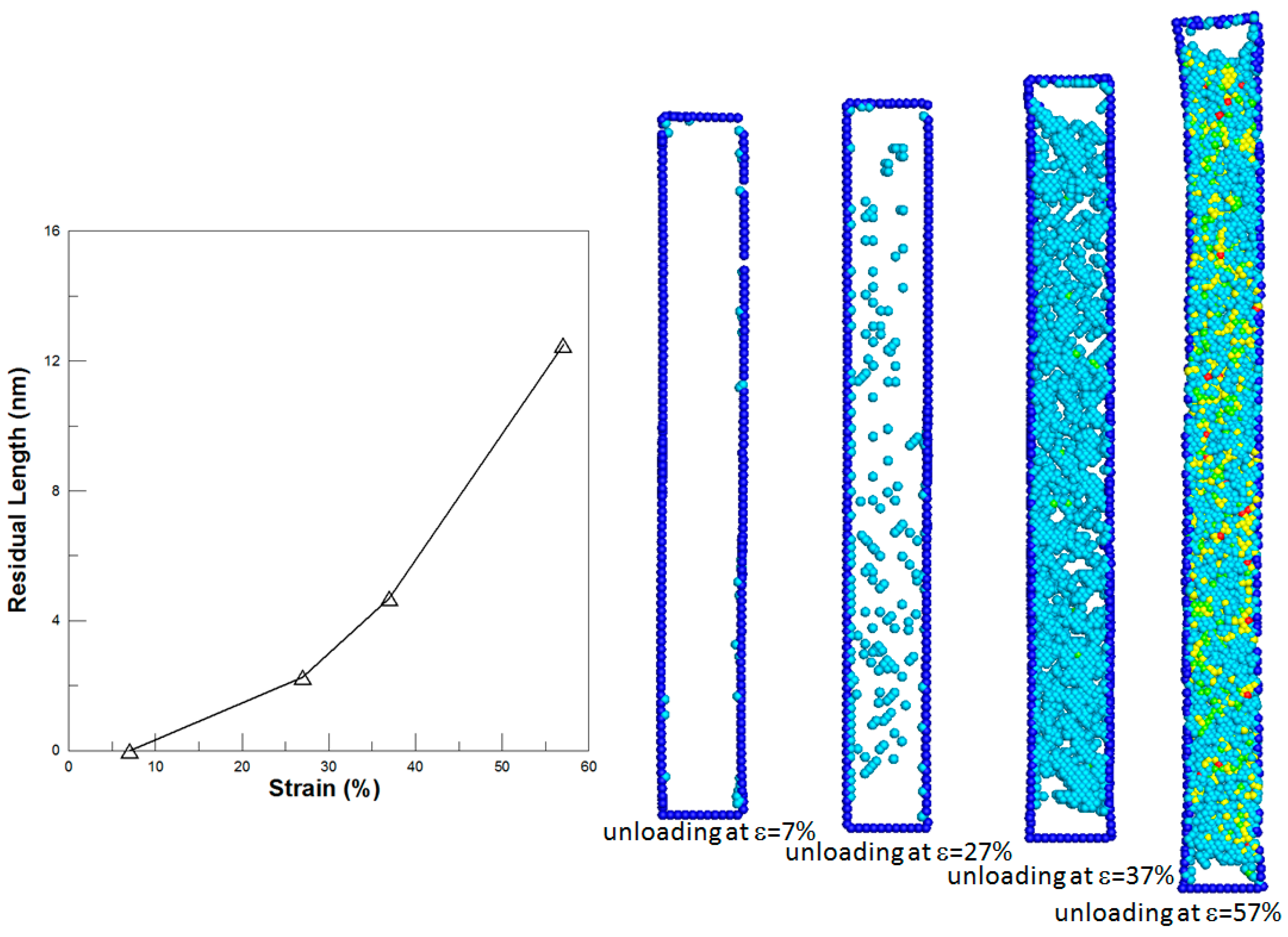
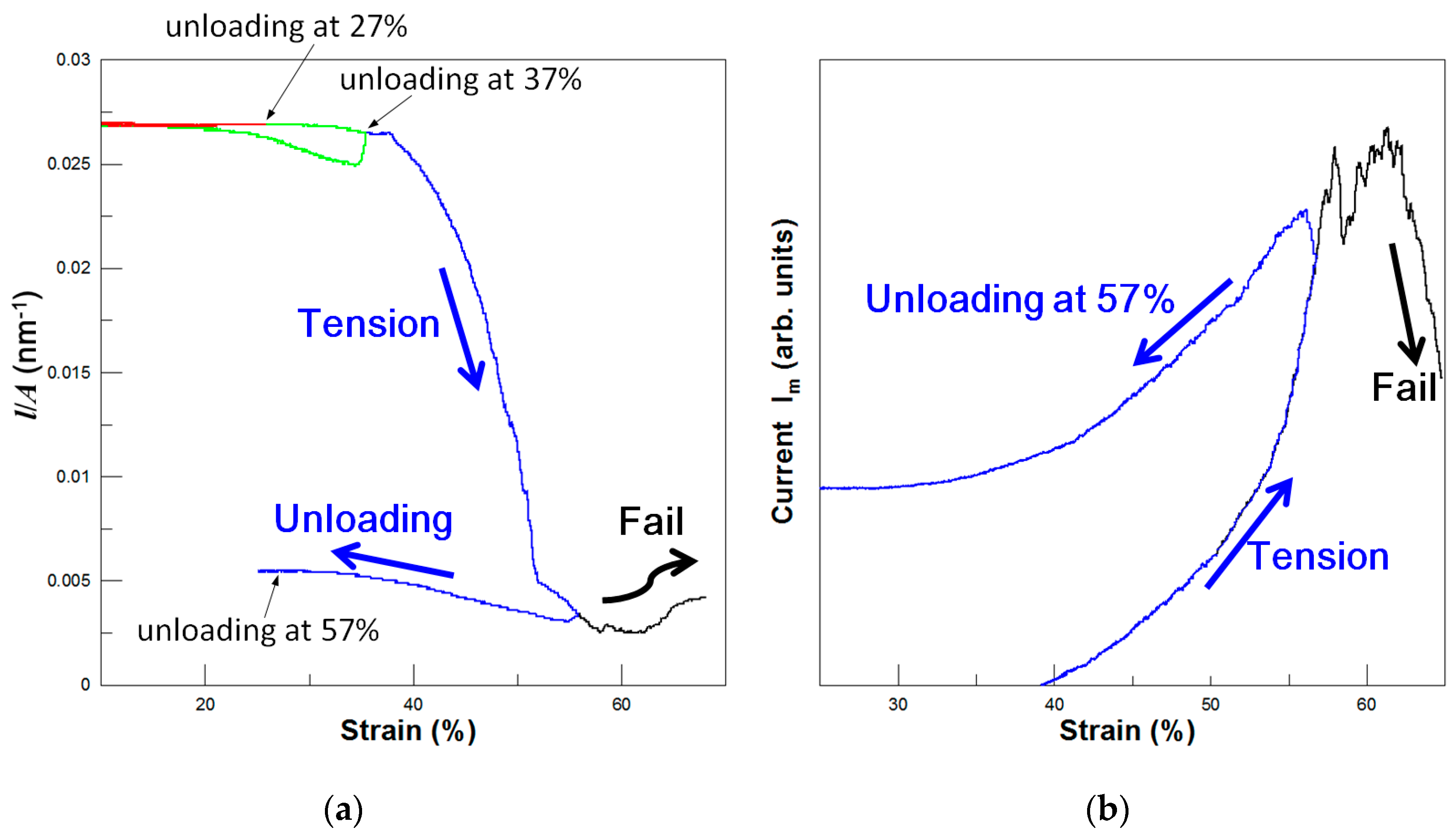
3.3. Effects of Unloading
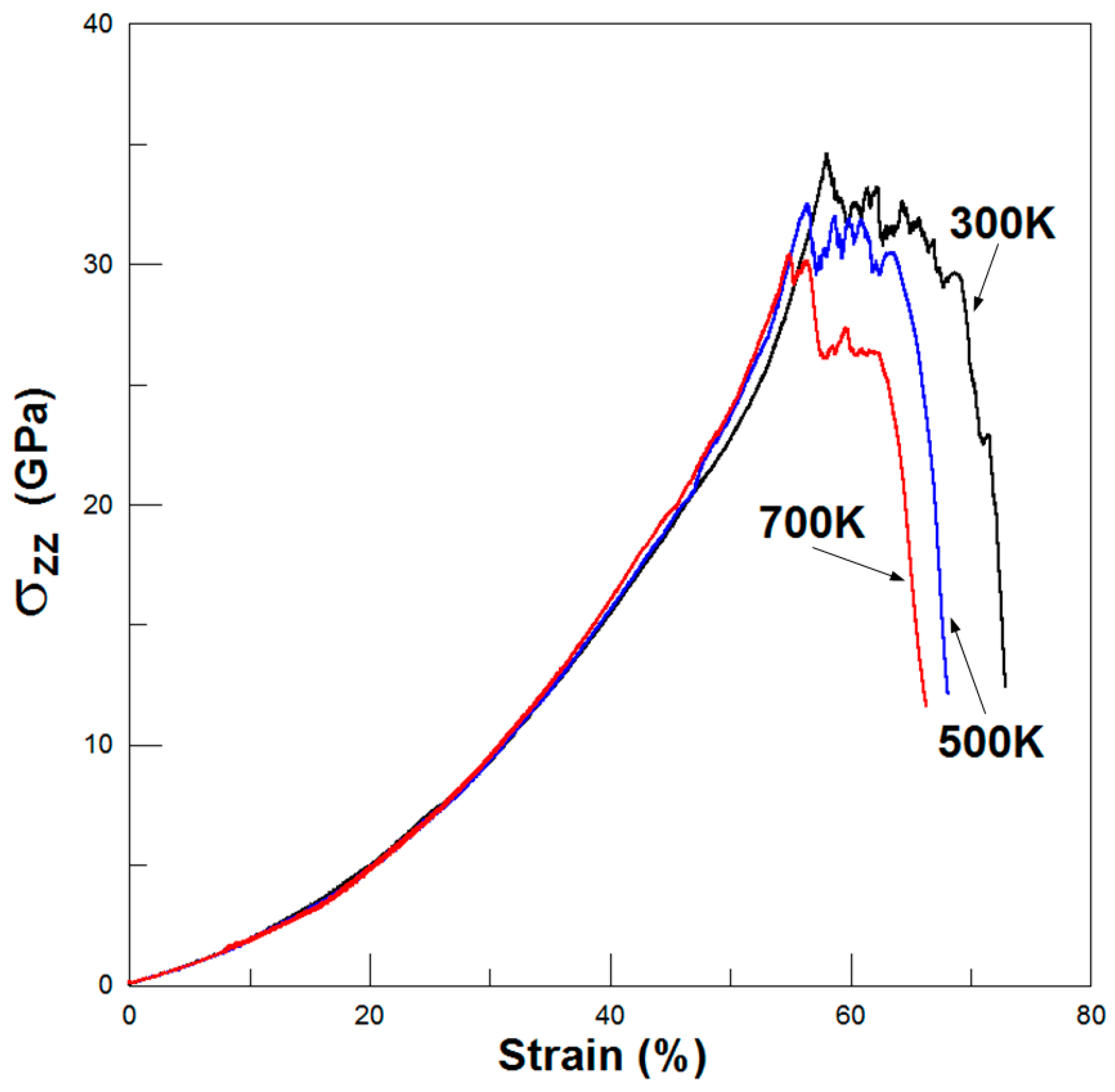
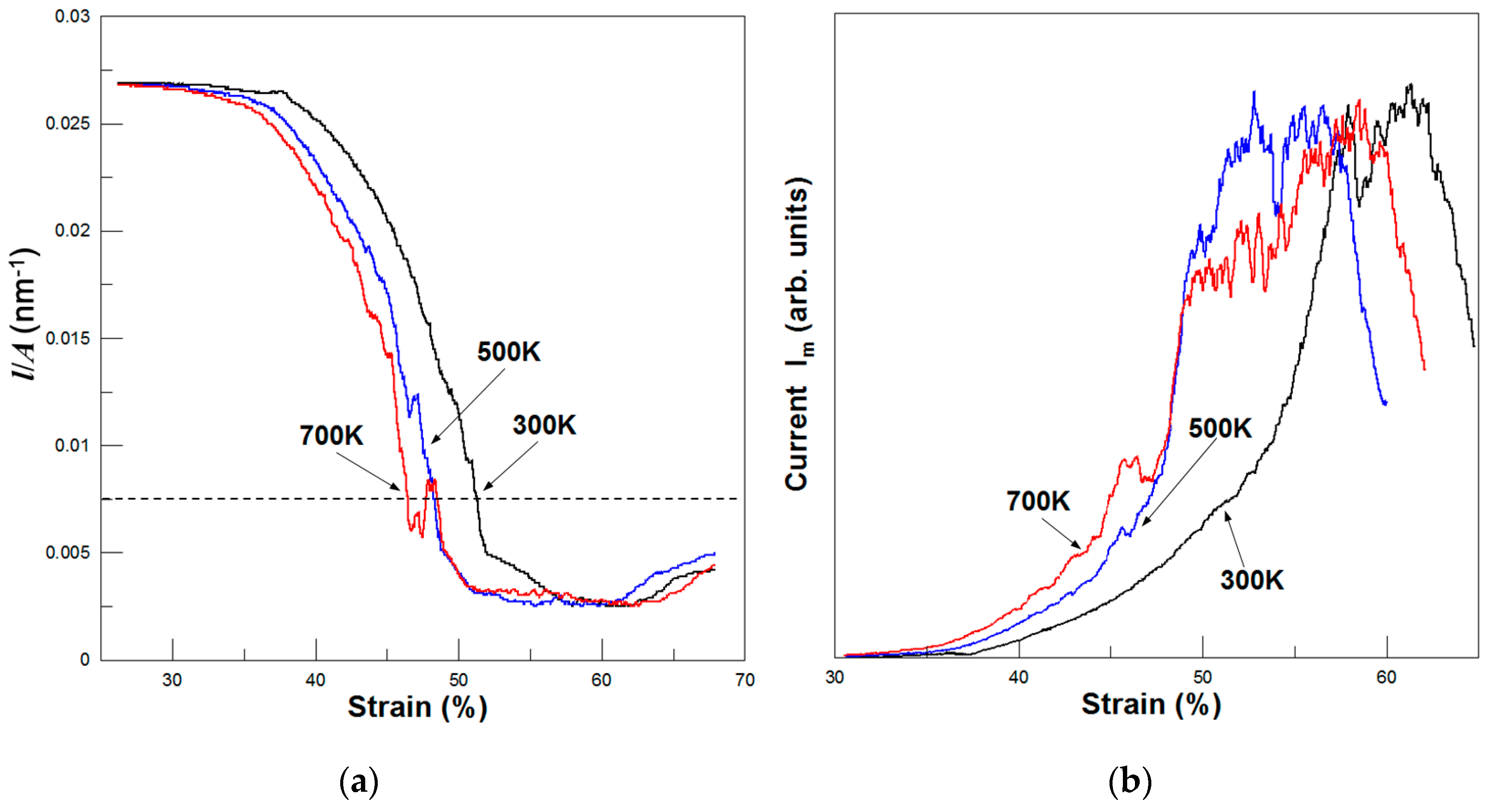
3.4. Effects of Temperature
4. Conclusions
Author Contributions
Funding
Conflicts of Interest
References
- Wang, M.H.; You, S.Y.; Wang, F.N.; Liu, Q. Effect of dynamic adjustment of diamond tools on nano-cutting behavior of single-crystal silicon. Appl. Phys. A 2019, 125, 1–13. [Google Scholar] [CrossRef]
- Wang, J.; Zhang, X.; Fang, F.; Chen, R. A numerical study on the material removal and phase transformation in the nanometric cutting of silicon. Appl. Surf. Sci. 2018, 455, 608–615. [Google Scholar] [CrossRef]
- Jelenković, E.V.; To, S. Suppression of nanoindentation-induced phase transformation in crystalline silicon implanted with hydrogen. Electron. Mater. Lett. 2017, 13, 393–397. [Google Scholar] [CrossRef]
- Stach, E.A.; Freeman, T.; Minor, A.M.; Owen, D.K.; Cumings, J.; Wall, M.A.; Chraska, T.; Hull, R.; Morris, J.W.; Zettl, A., Jr.; et al. Development of a nanoindenter for in situ transmission electron microscopy. Microsc. Microanal. 2001, 7, 507–517. [Google Scholar]
- Bobji, M.S.; Ramanujan, C.S.; Pethica, J.B.; Inkson, B.J. A miniaturized TEM nanoindenter for studying material deformation in situ. Meas. Sci. Technol. 2006, 17, 1324–1329. [Google Scholar] [CrossRef]
- Cheong, W.C.D.; Zhang, L.C. Molecular dynamics simulation of phase transformation in silicon monocrystals due to nano-indentation. Nanotechnology 2000, 11, 173–180. [Google Scholar] [CrossRef]
- Lin, Y.H.; Chen, T.C.; Yang, P.F.; Jian, S.R.; Lai, Y.S. Atomic-level simulations of nanoindentation-induced phase transformation in monocrystalline silicon. Appl. Surf. Sci. 2007, 254, 1415–1422. [Google Scholar] [CrossRef]
- Lin, Y.H.; Chen, T.C. A molecular dynamics study of phase transformation in monocrystalline Si under nanoindentation. Appl. Phys. A 2008, 92, 571–578. [Google Scholar]
- Lin, Y.H.; Jian, S.R.; Lai, Y.S.; Yang, P.F. Molecular dynamics simulation of nanoindentation-induced mechanical deformation and phase transformation in monocrystalline silicon. Nanoscale Res. Lett. 2008, 3, 71–75. [Google Scholar] [CrossRef]
- Kim, D.E.; Oh, S.I. Atomistic simulation of structural phase transformations in monocrystalline silicon induced by nanoindentation. Nanotechnology 2006, 17, 2259–2263. [Google Scholar] [CrossRef]
- Kim, D.E.; Oh, S.I. Deformation pathway to high-pressure phases of silicon during nanoindentation. J. Appl. Phys. 2008, 104, 013502. [Google Scholar] [CrossRef]
- Bradby, J.E.; Williams, J.S. In situ electrical characterization of phase transformations in Si during indentation. Phys. Rev. B 2003, 67, 085205. [Google Scholar] [CrossRef]
- Haberl, B.; Bradby, J.E.; Ruffell, S.; Williams, J.S. Phase transformations induced by spherical indentation in ion-implanted amorphous silicon. J. Appl. Phys. 2006, 100, 013520. [Google Scholar] [CrossRef]
- Ruffell, S.; Bradby, J.E.; Williams, J.S. An in situ electrical measurement technique via a conducting diamond tip for nanoindentation in silicon. J. Mater. Res. 2007, 22, 578–586. [Google Scholar] [CrossRef]
- Mylvaganam, K.; Zhang, L.C.; Eyben, P.; Mody, J.; Vandervorst, W. Evolution of metastable phases in silicon during nanoindentation: Mechanism analysis and experimental verification. Nanotechnology 2009, 20, 305705. [Google Scholar] [CrossRef]
- Seike, A.; Tange, T.; Sugiura, Y.; Tsuchida, I.; Ohta, H.; Watanabe, T.; Kosemura, D.; Ogura, A. Strain-induced transconductance enhancement by pattern dependent oxidation in silicon nanowire field-effect transistors. Appl. Phys. Lett. 2007, 91, 202117. [Google Scholar] [CrossRef]
- Zhuo, X.R.; Beom, H.G. Effect of side surface orientation on the mechanical properties of silicon nanowires: A molecular dynamics study. Crystals 2019, 9, 102. [Google Scholar] [CrossRef]
- Zarudi, I.; Zhang, L.C.; Cheong, W.C.D.; Yu, T.X. The difference of phase distributions in silicon after indentation with Berkovich and spherical indenters. Acta Mater. 2005, 53, 4795–4800. [Google Scholar] [CrossRef]
- Callahan, D.L.; Morris, J.C. The extent of phase transformation in silicon hardness indentations. J. Mater. Res. 1992, 7, 1614–1617. [Google Scholar] [CrossRef]
- Domnich, V.; Gogotsi, Y. Effect of phase transformations on the shape of the unloading curve in the nanoindentation of silicon. Appl. Phys. Lett. 2000, 76, 2214–2216. [Google Scholar] [CrossRef]
- Zhang, L.C.; Tanaka, H. On the mechanics and physics in the nano-indentation of silicon monocrystals. JSME Int. J. A 1999, 42, 546–559. [Google Scholar] [CrossRef]
- Cheong, W.C.D.; Zhang, L.C. Effect of repeated nano-indentations on the deformation in monocrystalline silicon. J. Mater Sci. Lett. 2000, 19, 439–442. [Google Scholar] [CrossRef]
- Zhu, Y.; Xu, F.; Qin, Q.; Fung, W.Y.; Lu, W. Mechanical properties of vapor-liquid-solid synthesized silicon nanowires. Nano Lett. 2009, 9, 3934–3939. [Google Scholar] [CrossRef] [PubMed]
- Tekleab, D.; Carroll, D.L.; Samsonidze, G.G.; Yakobson, B.I. Strain-induced electronic property heterogeneity of a carbon nanotube. Phys. Rev. B 2001, 64, 035419. [Google Scholar] [CrossRef]
- Cohen-Karni, T.; Segev, L.; Srur-Lavi, O.; Cohen, S.R.; Joselevich, E. Torsional electromechanical quantum oscillations in carbon nanotubes. Nat. Nanotechnol. 2006, 1, 36–41. [Google Scholar] [CrossRef]
- He, R.R.; Yang, P.D. Giant piezoresistance effect in silicon nanowires. Nat. Nanotechnol. 2006, 1, 42–46. [Google Scholar] [CrossRef]
- Karvounis, A.; Gholipour, B.; MacDonald, K.F.; Zheludev, N.I. Giant electro-optical effect through electrostriction in a nanomechanical metamaterial. Adv. Mater. 2019, 31, 1–6. [Google Scholar] [CrossRef] [PubMed]
- Kang, K.; Cai, W. Brittle and ductile fracture of semiconductor nanowires-molecular dynamics simulations. Philos. Mag. 2007, 87, 2169–2189. [Google Scholar] [CrossRef]
- Komanduri, R.; Chandrasekaran, N.; Raff, L.M. Molecular dynamic simulations of uniaxial tension at nanoscale of semiconductor materials for micro-electro-mechanical systems (MEMS) applications. Mater. Sci. Eng. A 2003, 340, 58–67. [Google Scholar] [CrossRef]
- Jing, Y.; Meng, Q.; Zhao, W. Molecular dynamics simulations of the tensile and melting behavior of silicon nanowire. Phys. E 2009, 41, 685–689. [Google Scholar] [CrossRef]
- Han, X.; Zheng, K.; Zhang, Y.; Zhang, X.; Zhang, Z.; Wang, L. Low-temperature in situ large-strain plasticity of silicon nanowires. Adv. Mater. 2007, 19, 2112–2118. [Google Scholar] [CrossRef]
- Tersoff, J. New empirical model for the structural properties of silicon. Phys. Rev. Lett. 1986, 56, 632–635. [Google Scholar] [CrossRef]
- Tersoff, J. New empirical approach for the structure and energy of covalent systems. Phys. Rev. B 1988, 37, 6991–7000. [Google Scholar] [CrossRef]
- Tersoff, J. Empirical interatomic potential for silicon with improved elastic properties. Phys. Rev. B 1988, 38, 9902–9905. [Google Scholar] [CrossRef]
- Tersoff, J. Empirical interatomic potential for carbon, with applications to amorphous carbon. Phys. Rev. Lett. 1988, 61, 2879–2882. [Google Scholar] [CrossRef] [PubMed]
- Tersoff, J. Modeling solid-state chemistry: Interatomic potentials for multicomponent systems. Phys. Rev. B 1989, 39, 5566–5568. [Google Scholar] [CrossRef]
- Zhang, L.C.; Tanaka, H. Towards a deeper understanding of friction and wear on the atomic scale: A molecular dynamics analysis. Wear 1997, 211, 44–53. [Google Scholar] [CrossRef]
- Zhang, L.C.; Tanaka, H. Atomic scale deformation in silicon monocrystals induced by two-body and three-body contact sliding. Tribol. Int. 1998, 31, 425–433. [Google Scholar] [CrossRef]
- Tanaka, H.; Zhang, L.C. Phase transformation of silicon during nanoindentication. In Advances in Abrasive Technology; Zhang, L.C., Yasunaga, N., Eds.; World Scientific: Sydney, Australia, 1997; pp. 43–47. [Google Scholar]
- Iwaki, T. Molecular dynamics study on stress-strain in very thin film. JSME Int. J. A 1996, 39, 346–353. [Google Scholar]
- Lin, Y.C.; Pen, D.J. Atomistic behavior analysis of Cu nanowire under uniaxial tension with maximum local stress method. Mol. Simul. 2007, 33, 979–988. [Google Scholar] [CrossRef]
- Lin, Y.C.; Pen, D.J. Analogous mechanical behaviors in <100> and <110> directions of Cu nanowires under tension and compression at a high strain rate. Nanotechnology 2007, 18, 395705. [Google Scholar] [CrossRef] [PubMed]
- Miyazaki, N.; Shiozaki, S. Calculation of mechanical properties of solids using molecular dynamics method. JSME Int. J. A 1996, 39, 606–613. [Google Scholar] [CrossRef]
- Kelchner, C.L.; Plimpton, S.J.; Hamilton, J.C. Surface step effects on nanoindentation. Phys. Rev. B 1998, 58, 11085–11088. [Google Scholar] [CrossRef]
- Tschopp, M.A.; Spearot, D.E.; McDowell, D.L. Atomistic simulations of homogeneous dislocation nucleation in single crystal copper. Model. Simul. Mater. Sci. Eng. 2007, 15, 693–709. [Google Scholar] [CrossRef]
- Capolungo, L.; Spearot, D.E.; Cherkaoui, M.; McDowell, D.L.; Qu, J.; Jacob, K.I. Dislocation nucleation from bicrystal interface and grain boundary ledges: Relationship to nanocrystalline deformation. J. Mech. Phys. Solids 2007, 55, 2300–2327. [Google Scholar] [CrossRef]
- Tschopp, M.A.; Tucker, G.J.; McDowell, D.L. Atomistic simulations of tension-compression asymmetry in dislocation nucleation for copper grain boundaries. Comput. Mater. Sci. 2008, 44, 351–362. [Google Scholar] [CrossRef]
- Tschopp, M.A.; McDowell, D.L. Grain boundary dislocation sources in nanocrystalline copper. Scr. Mater. 2008, 58, 299–302. [Google Scholar] [CrossRef]
- Tschopp, M.A.; McDowell, D.L. Influence of single crystal orientation on homogeneous dislocation nucleation under uniaxial loading. J. Mech. Phys. Solids 2008, 56, 1806–1830. [Google Scholar] [CrossRef]
- Lee, Y.; Park, J.Y.; Kim, S.Y.; Jun, S.; Im, S. Atomistic simulations of incipient plasticity under Al (111) nanoindentation. Mech. Mater. 2005, 37, 1035–1048. [Google Scholar] [CrossRef]
- Pei, Q.X.; Lu, C.; Liu, Z.S.; Lam, K.Y. Molecular dynamics study on the nanoimprint of copper. J. Phys. D Appl. Phys. 2007, 40, 4928–4935. [Google Scholar] [CrossRef]
- Chen, H.P.; Kalia, R.K.; Nakano, A.; Vashishta, P. Multimillion-atom nanoindentation simulation of crystalline silicon carbide: Orientation dependence and anisotropic pileup. J. Appl. Phys. 2007, 102, 063514. [Google Scholar] [CrossRef]
- Izumi, S.; Yip, S. Dislocation nucleation from a sharp corner in silicon. J. Appl. Phys. 2008, 104, 03351. [Google Scholar] [CrossRef]
- Deb, S.K.; Wilding, M.; Somayazulu, M.; McMillan, P.F. Pressure-induced amorphization and an amorphous-amorphous transition in densified porous silicon. Nature 2001, 414, 528–530. [Google Scholar] [CrossRef] [PubMed]


© 2019 by the authors. Licensee MDPI, Basel, Switzerland. This article is an open access article distributed under the terms and conditions of the Creative Commons Attribution (CC BY) license (http://creativecommons.org/licenses/by/4.0/).
Share and Cite
Lin, Y.-H.; Chen, T.-C. Nanoscale Mechanical and Mechanically-Induced Electrical Properties of Silicon Nanowires. Crystals 2019, 9, 240. https://doi.org/10.3390/cryst9050240
Lin Y-H, Chen T-C. Nanoscale Mechanical and Mechanically-Induced Electrical Properties of Silicon Nanowires. Crystals. 2019; 9(5):240. https://doi.org/10.3390/cryst9050240
Chicago/Turabian StyleLin, Yen-Hung, and Tei-Chen Chen. 2019. "Nanoscale Mechanical and Mechanically-Induced Electrical Properties of Silicon Nanowires" Crystals 9, no. 5: 240. https://doi.org/10.3390/cryst9050240
APA StyleLin, Y.-H., & Chen, T.-C. (2019). Nanoscale Mechanical and Mechanically-Induced Electrical Properties of Silicon Nanowires. Crystals, 9(5), 240. https://doi.org/10.3390/cryst9050240