1. Introduction
Gallium Nitride (GaN) is a III-V group compound semiconductor. It can exist in either wurtzite form or zinc-blende form. The wurtzite modification of GaN is slightly more common and has a wide direct band gap of 3.4 eV at room temperature [
1]. The direct band gap enables the use of GaN for highly efficient light emitting diodes (LEDs) [
2], laser diodes (LDs), and UV detectors. In the last fifteen years, the efficiency of GaN-based LEDs has improved greatly, making solid state lighting available [
3]. GaN offers several other attractive properties, including a high breakdown field, E
B = 4.0 MV/cm, a high electron mobility, μ = 1300
, and a large dielectric constant of ε = 9.0. These parameters combined with the large band gap make GaN an excellent candidate for high power RF devices [
4,
5]. Gallium Nitride (GaN) is also well suited for bio-sensor applications due to its chemical stability, wide spectral transmission window, and biocompatibility [
6]. Although dry etching using inductively coupled plasma (ICP) has been employed in the past [
7], deep etching of up to 5 μm of thick GaN films is rare. More recently GaN has attracted increased interest for integrated photonic applications [
8,
9].
For waveguide application employing evanescent excitation, a low surface roughness of the waveguide and a sharp etching profile are essential. For optical coupling from the end-face of the GaN waveguide, the cross-section of the waveguide needs to be in the range of microns. Therefore, deep etching a thick GaN film to create a waveguide structure is of significant interest.
Using a conventional photoresist as an etching barrier does not provide enough depth for a GaN waveguide. If the photoresist is not sufficiently thick in spin coating, it will not effectively block the ion bombardment during the inductively coupled plasma (ICP) etching. This causes over-etching of the waveguide, reducing not only the height of the waveguide, but also creating a rough surface as a result of ion bombardment. On the other hand, if an excessively thick coating of photoresist is formed, the exposure and development process will be non-uniform, leading to the poor development of the photoresist and preventing the fabrication of the waveguide. A denser and more uniform material is required as an etch barrier to improve the etching process. Tetraethyl Orthosilicate (TEOS), due to its excellent step coverage, is the reactive gas widely used in chemical vapor deposition to deposit a dense and uniform silicon oxide film. TEOS has a favorable surface mobility and gap-filling ability [
10,
11,
12]. Therefore, TEOS deposited oxide is used and studied as the etching barrier for deep etching in the present work. Various widths of GaN waveguides were experimentally fabricated.
2. Experimental Section
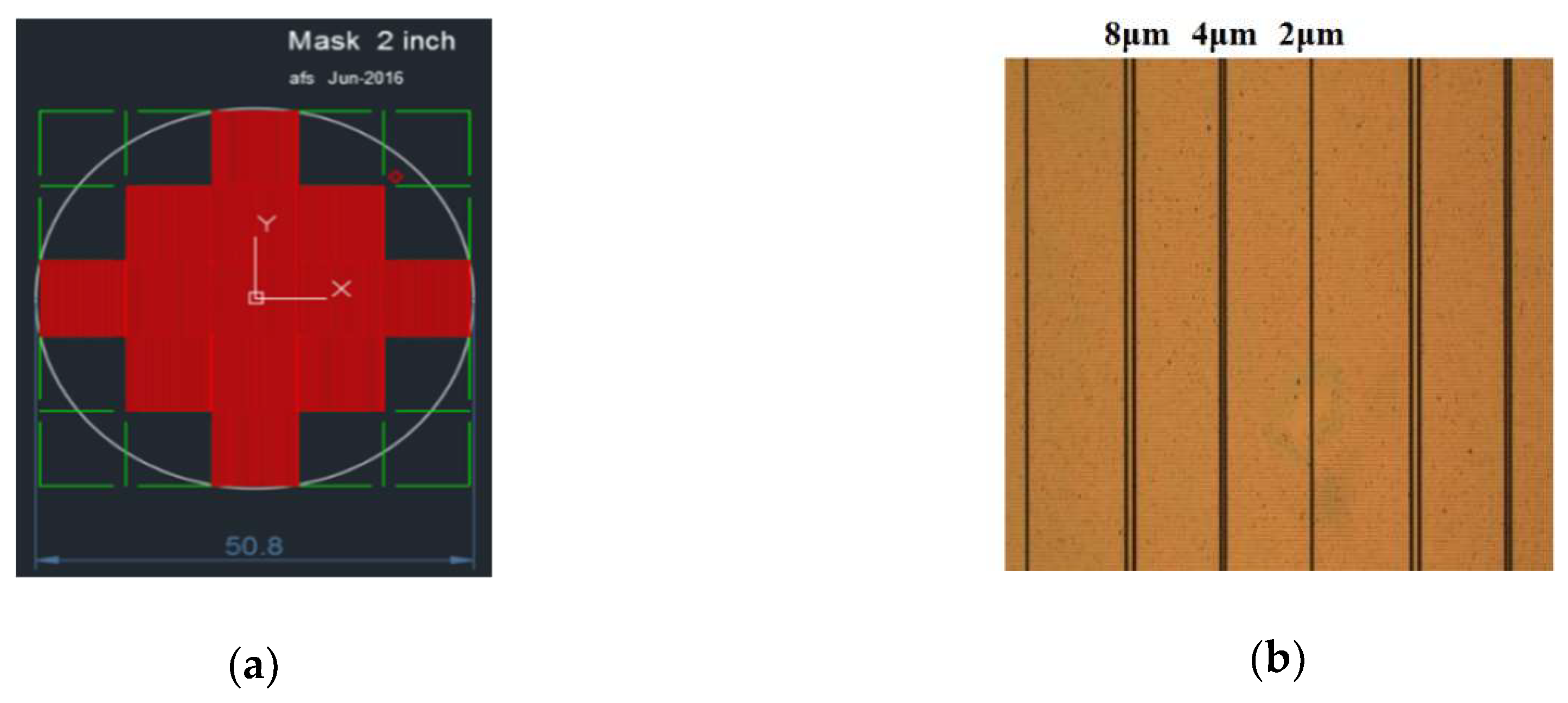
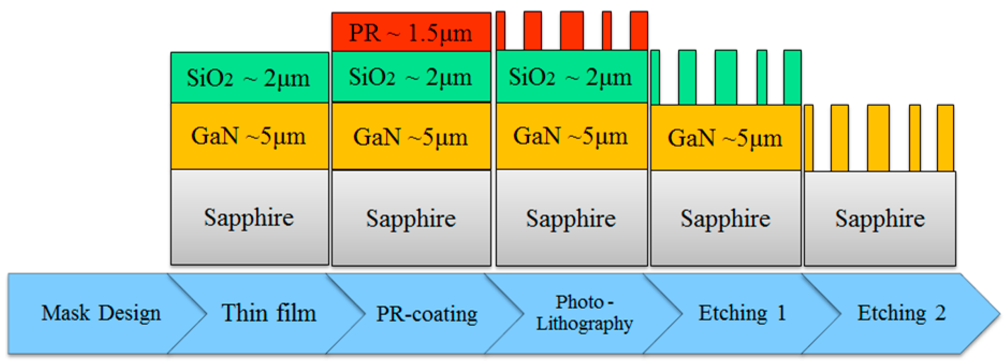
Initially, a 2-inch mask was constructed with waveguide patterns at various widths, as shown in
Figure 1a. After that, commercial 2-inch sapphire substrates with a 5 μm GaN thin film epitaxially grown by MOCVD were cleaned with a standard RCA procedure in an ultrasonic bath with acetone, isopropanol and de-ionized water for 3 minutes each sequentially. Subsequently, 2 μm of Tetraethyl Orthosilicate (TEOS) oxide was deposited to form the SiO
2 layer on top of the wafers as the first etching barrier by plasma enhanced chemical vapor deposition (PECVD). Next, a PR-5214 photoresist with a thickness of 1.5 μm was spin-coated on the substrate wafers. An exposure system was used to develop the desired waveguide patterns (2, 4 and 8 μm, respectively), as shown in
Figure 1b.
After the deposition of the etching barriers, wafers were etched using an inductively coupled plasma reactive ion etching system. This created a deep-etched GaN waveguide structure. All of the etching parameters of the system such as the ICP source power, RF bias power, chamber pressure and gas flows were optimized in the experiment. The fabricated GaN waveguide structure was characterized by a stylus profilometer (Alpha-Stepper; Surfcorder ET3000, Kosaka Laboratory Ltd., Tokyo, Japan), a field emission scanning electron microscope (SEM; SU8220, Hitachi High-Technologies, Tokyo, Japan and JSM-7500F, JEOL, Tokyo, Japan), an energy dispersive X-ray spectrometer (EDS; INCA X-ACT, OXFORD, High Wycombe, UK), and an atomic force microscope (AFM; NT-MDT Solver P47, NT-MDT Spectrum Instruments, Moscow, Russia).
3. Results and Discussion
Inductively coupled plasma reactive ion etching (ICP-RIE etching) to create an anisotropic GaN etching depth up to 5 μm is not well understood [
13,
14]. The choices of the etching-resistant material, etching gas, and etching time are crucial to ensure the success of the etching process. If the etching time is too long, then the waveguide will be partially etched. This results in an uneven waveguide surface and scattering of the laser signal due to surface roughness in the waveguide. If the etching time is too short, the isolated waveguide cannot form, which will cause some loss of signal [
15].
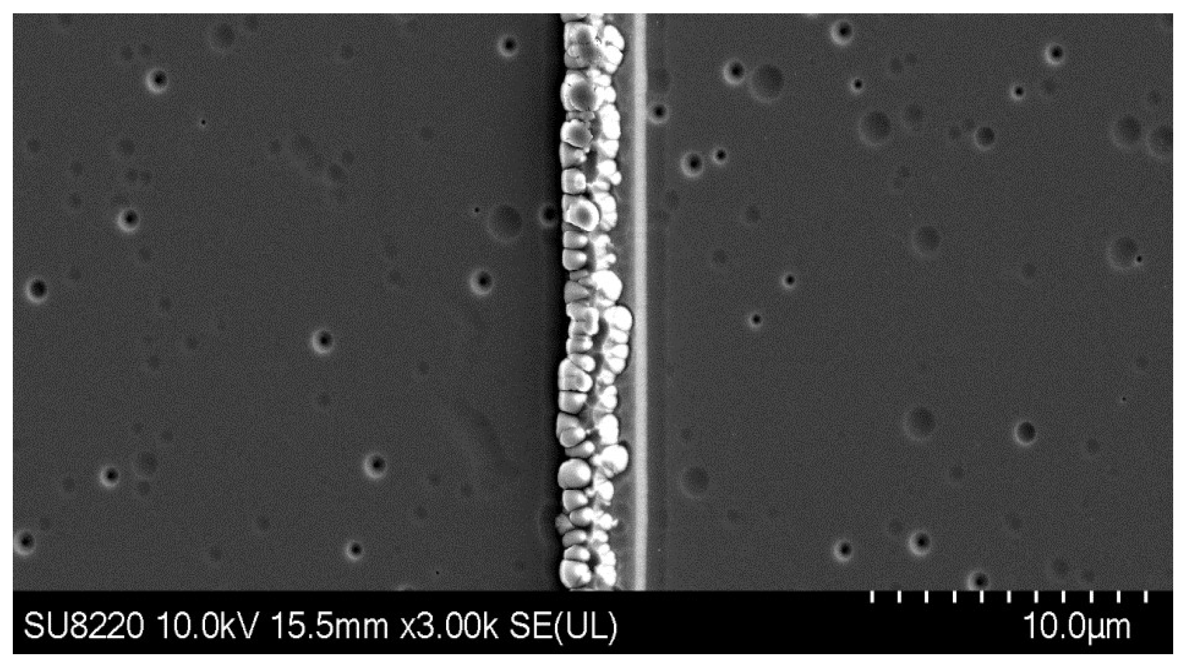
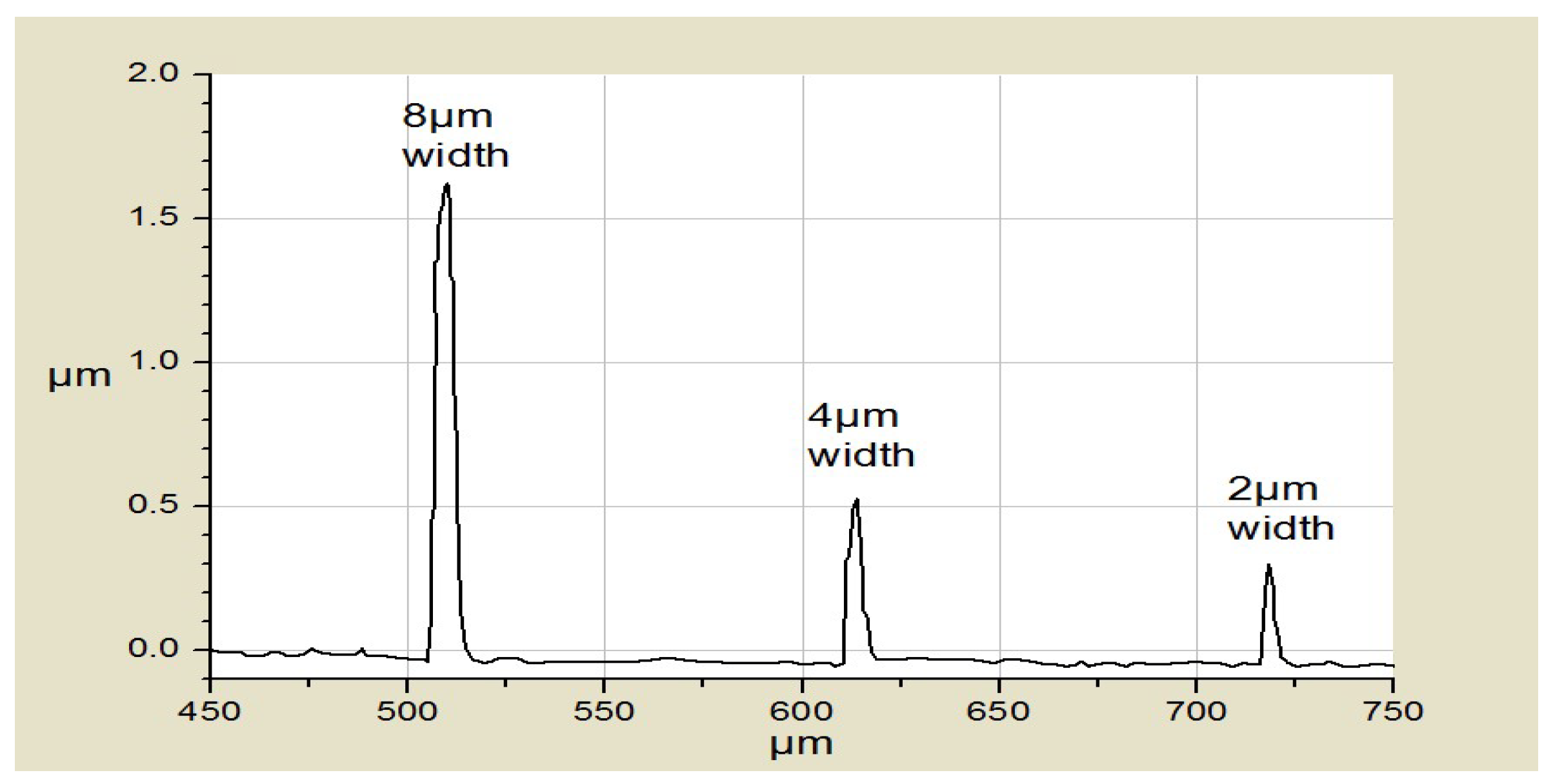
The top of the sapphire substrate was covered with a 5 μm thick GaN epilayer. Initially, only one single photoresist (PR) layer was used as an etching barrier. To shape the perfect waveguide with etching to the sapphire substrate, a long etching time (1500 s) was used. However, after the etching process, the etching resistance of the PR mask was neither as expected nor sufficient to provide a deep etch of 5 μm in the GaN. The resulting waveguide displayed a damaged surface and damaged side walls, as shown in
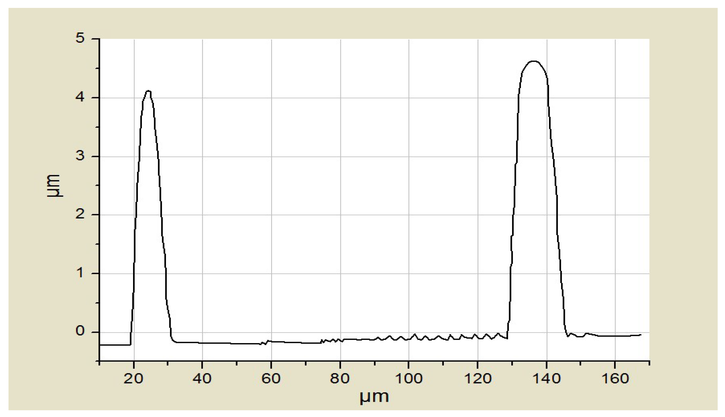
Figure 2. This is clearly unacceptable for use as a waveguide. In addition, the waveguides were characterized with a profilometer. The surface profiles are shown in
Figure 3. The height of the waveguide is not uniform, and the non-uniform exposure has almost destroyed the 2 μm wide waveguide.
In order to improve the etching process, an extra oxide layer of TEOS, which acted as a precursor for the deposition of SiO
2, was deposited on top of the GaN layer by PECVD before the photoresist coating. After the development of the photoresist coating, Ar and CF
4 gases were used as etchants to remove the photoresist barrier layer while the SiO
2 layer acted as an etch barrier to protect the GaN. Since the SiO
2 layer is relatively stable in the etching process, it blocks etching gases such as Cl
2 and BCl
3.
Figure 4 shows the etching process. To improve the deep etching and to reduce the complexity of the process, the relevant parameters were optimized. In the initial stage of the experiment, a selectivity ratio of 1:1 of the photoresist to GaN was chosen. However, a spin-coating photoresist with a thickness of 5 μm is difficult to form in the lithography process. SiO
2 was added to the photoresist layer in the manufacturing process. SiO
2, deposited by PECVD as an ICP etching barrier, is commonly used in semiconductor processing and exhibits an excellent deposition uniformity at high selectivity ratios. Therefore, Ar and CF
4 gases were first used to etch out the layer pattern of the SiO
2 barrier. Subsequently, Cl
2 and BCl
3 gases were used to etch the GaN layer with the etching parameters listed in
Table 1.
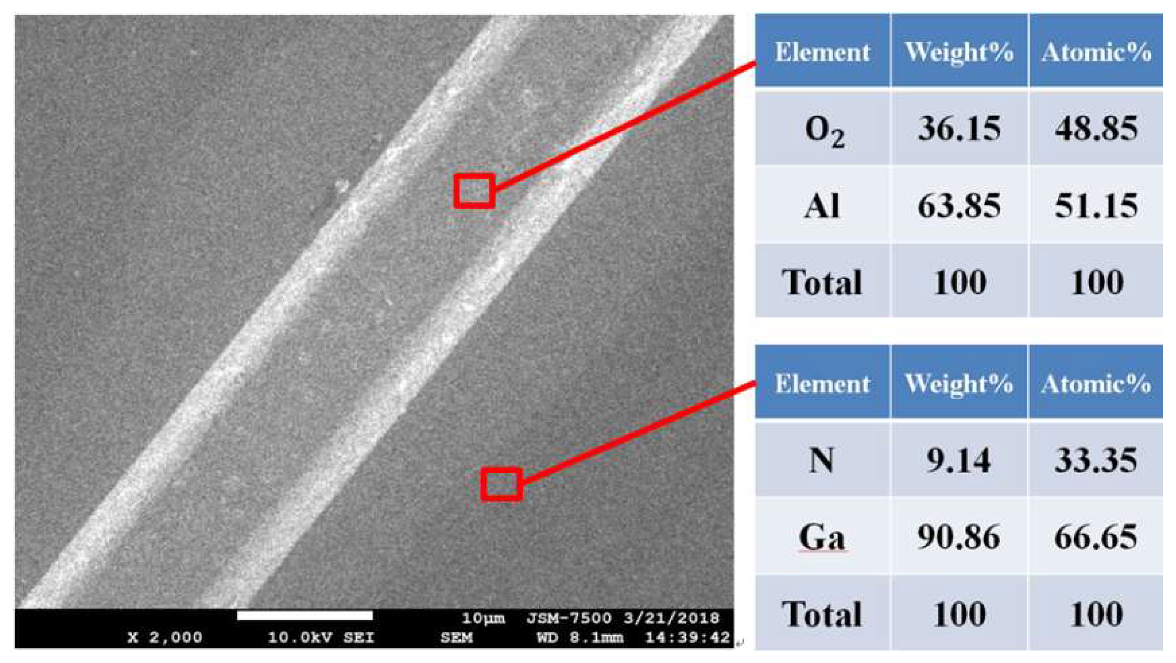
Figure 5 displays a FESEM image and elemental atomic percentage of a GaN waveguide coated with an SiO
2 layer as an etching barrier. The etching time was 1500 seconds. A comparison of
Figure 2 and
Figure 5 demonstrates that an extra oxide layer, SiO
2, greatly reduced the roughness of the GaN waveguide surface (for a fixed etching time of 1500 s), and enabled a 5 μm-deep GaN etching of the sapphire substrate. Etching parameter combinations should be analyzed in the future to optimize results. The scanning electron microscopy (SEM; JSM-7500F, JEOL, Tokyo, Japan) image and elemental composition (energy dispersive spectroscopy, EDS; INCA X-ACT, OXFORD, High Wycombe, UK) in
Figure 5 indicate the success of the above process with proper etch selectivity ratios to produce the desired GaN waveguide.
Figure 6 displays the results of a 5 μm-deep etching. Through this process, a useful GaN waveguide was fabricated.
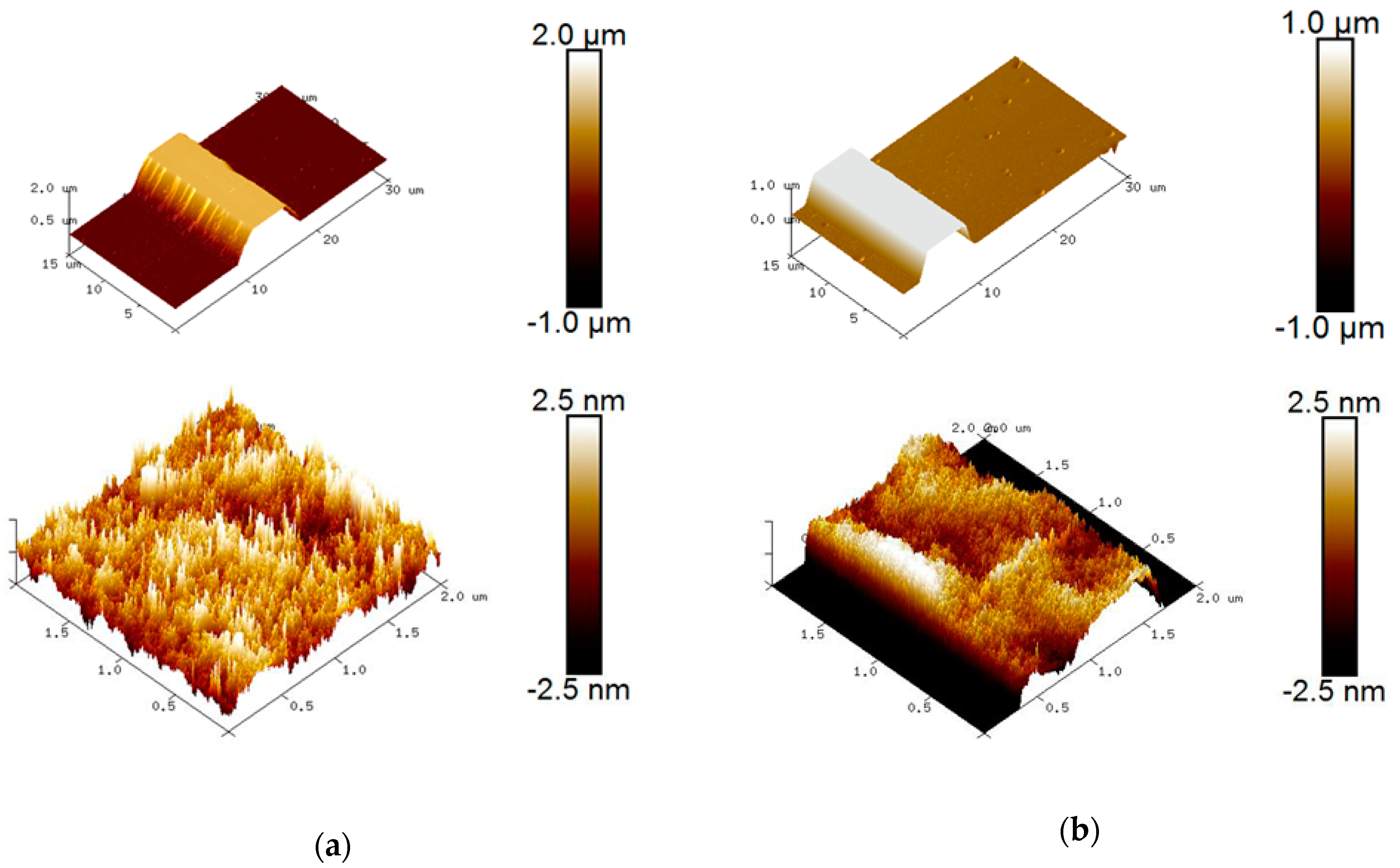
Both the steepness and the surface roughness of the waveguides are characterized.
Figure 7a,b shows the 3D images of the fabricated waveguide without the SiO
2 layer in the etching process and with it, respectively. All 3D waveguide images were obtained with an atomic force microscope (AFM; NT-MDT Solver P47, NT-MDT Spectrum Instruments, Moscow, Russia) system in the Taiwan Semiconductor Research Institute (TSRI). A similar surface roughness and sidewall properties were observed in the GaN waveguide with the SiO
2 layer during etching. This also indicates that the SiO
2 layer, when used as an etching barrier, is an effective method for fabricating GaN waveguides.
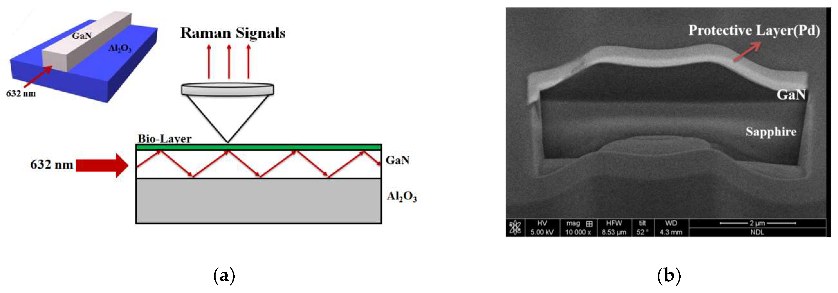
We emphasize that the focus of the current report is the fabrication of the waveguide device. However, to illustrate future applications, we show in a schematic diagram (
Figure 8a), how this device can be used for evanescently excited Raman spectroscopy from extremely thin bio-samples. The excitation source is coupled into the waveguide through the end-face. In
Figure 8b, a cross-sectional view of the waveguide is depicted. The guided wave of the excitation source can propagate through the thin sample along the direction of the waveguide, evanescently exciting the thin bio-layer on top of the waveguide. The Raman scattered light is collected in a 90° geometry from the top of the waveguide.
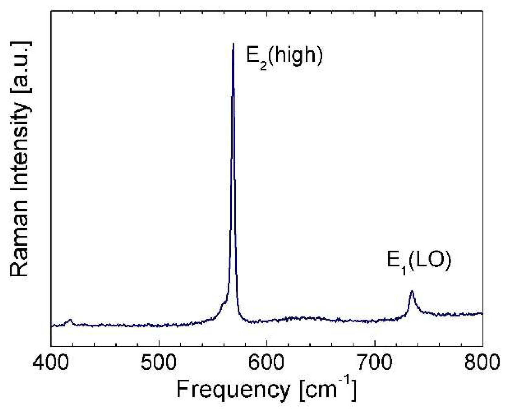
Figure 9 displays a Raman spectrum of a GaN waveguide structure using a micro-Raman setup. The excitation wavelength was 632 nm. We observe vibrational bands at 567 cm
−1 and 735 cm
−1 that are assigned to the E
2(high) and E
1(LO) modes, respectively [
16]. The shoulder at 560 cm
−1 is attributed to the E
1(TO) mode. These vibrational modes are characteristic of the GaN wurtzite structure.
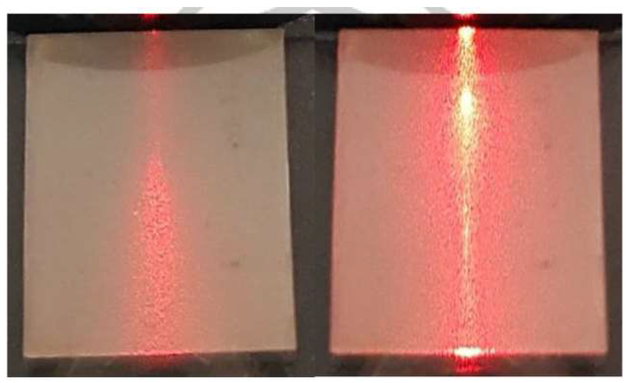
Due to the high refractive index of GaN, coupling into the waveguide using prisms poses difficulties. Therefore, the beam from a Helium-Neon laser was injected into the waveguide by end-face coupling via a 20x microscope objective. However, achieving a high-efficiency coupling was not easy, as suitable angles of incidence and a small laser spot were required. The waveguide thickness was only about one percent of the substrate.
Figure 10 shows a well coupled beam in comparison to the uncoupled case. The propagation of the coupled beam is clearly seen in the right panel of
Figure 10. In particular, the cross section of the exiting beam is visible at the end-face. This indicates that the etching has resulted in a high quality GaN waveguide that can be further used for spectroscopy with evanescent excitation. Further studies to quantify the propagation and coupling losses are in progress.

 ,
, 


