Abstract
Hydrothermally grown TiO2 nanorods are a key material for several electronic applications. Due to its anisotropic crystal structure, the electronic properties of this semiconductor depend on the crystallographic direction. Consequently, it is important to control the crystal orientation to optimize charge carrier pathways. So far, the growth on common polycrystalline films such as fluorine tin oxide (FTO) results in randomly distributed growth directions. In this paper, we demonstrate the ability to control the growth direction of rutile TiO2 nanocrystals via the orientation of the seed crystals. The control of the orientation of such nanocrystals is an important tool to adjust the electronic, mechanical, and chemical properties of nanocrystalline films. We show that each employed macroscopic seed crystal provides the growth of parallel nanofingers along the [001] direction under specific angles. The parallel growth of these nanofingers leads to mesocrystalline films whose thickness and surface structure depends on the crystal orientation of the seed crystal. In particular, the structure of the films is closely linked with the known inner structure of hydrothermally grown rutile TiO2 nanorods on FTO. Additionally, comprehensive 1D structures on macroscopic single-crystals are generated by branching processes. These branched nanocrystals form expanded 2D defect planes, which provide the opportunity of defect doping-induced two-dimensional electronic systems (2DES).
1. Introduction
Rutile TiO2 nanostructures have versatile capabilities in applications such as photocatalysis, [1,2,3,4] surface wetting, [5,6,7] disinfection, [8,9] gas and molecule sensing, [10,11] displays, [12] transparent electrodes, [12] photodetectors, [13,14] photovoltaics, [15,16,17] fuel cells, [18] data storage, [19] capacitors, [20] batteries, [21,22,23,24] and medical engineering [25]. Often, these nanostructures are created using an inexpensive, fast, and scalable hydrothermal method [26]. Orientated TiO2 nanorod arrays can be grown hydrothermally on polycrystalline rutile fluorine tin oxide (FTO) films using the substrate as a seed layer [17]. These nanorods grow along the [001] direction with {110} facets on their side walls, {100} facets on their side edges, and {001} and {111} facets on their tips [27]. They exhibit a fine structure consisting of bundled nanofingers, which are aligned in parallel to the [001] direction. Hence, the nanofingers have the same shape and length as the nanorods, but they are significantly thinner. Previously, we found that the fine structure results from crystal defects in the early growth state and propagates throughout the growth [27]. The additional grain boundaries affect not only the chemical stability but also the electronic properties such as charge carrier mobility [28,29,30,31]. Within a nanorod, these nanofingers merge and form a single crystal for sufficiently high annealing temperatures [32].
Besides the fine structure, another important effect occurs, which offers great opportunities for electronic applications. The hydrothermal growth of rutile TiO2 nanorods is accompanied by branching events in the early growth stage. In as-grown nanorods, the principal crystal and the branch are separated by a thin 2D defect plane. The existence of flat defect planes in crystals gives rise for specific electronic applications. Such a defect layer represents a local change of the stoichiometry and a shift of the conduction band. Density functional theory (DFT) calculations performed by Morgan and Watson indicate a low formation energy of oxygen vacancies on specific interfaces [33]. Dependent on the kind of defect levels induced by such vacancies, the defect plane has either an n-n−-n or n-p-n type character [33,34].
In this study, we demonstrate that the growth direction and orientation is controllable via the crystallographic orientation of the seed crystal. Specifically, we performed the nanorod growth on macroscopic rutile TiO2 single crystals with defined crystal facets resulting in a similar fine structure as observed in the nanorods grown on polycrystalline seed films. Here, the orientation of the nanofingers along the [001] direction is used as an indicator for the crystallographic direction of the grown mesocrystalline films [21,27]. Besides the inner structure, nanorods and the presented mesocrystalline films share another feature. Branching, as typically observed for rutile TiO2 nanorods, [35] appear on the mesocrystalline films as well as provide expanded two-dimensional electron systems (2DES), [36] which have the potential for sensing and transistor applications [37,38].
2. Materials and Methods
The hydrothermal growth was performed on commercial rutile TiO2 single crystals (Latech Scientific Supply Pte. Ltd., Singapore) with polished {100}, {001}, {110}, and {111} facets fabricated by a float zone crystal growth method. For all crystals, the rms-roughness is less than 1 nm and the purity is above 99.99%. The hydrothermal growth was performed by heating a 20 mL of hydrochloric acid (HCl, reagent grade, VWR Chemicals, 14.8wt% concentration in distilled water) and 350 μL titanium(IV) butoxide (C16H36O4Ti, reagent grade, 97%, Sigma-Aldrich, now Merck KGaA, Darmstadt, Germany) solution in a Teflon lined autoclave at 180 °C. The growth process was stopped after 3 h by rapid quenching in water. After the growth, the samples were split mechanically and the edge was investigated with a scanning electron microscope (SEM). The field-effect scanning electron microscope (FE SEM) imaging was executed with a Zeiss CrossBeam 1540XB (Carl Zeiss Microscopy GmbH, Jena, Germany) using an acceleration voltage of 5 keV. Powdered X-ray diffraction (PXRD) data were acquired on a Bruker AXS D8 Discover (Bruker Corporation, Billerica, USA) with an IµS microfocus X-ray source (Cu-Kα radiation) equipped with a 2D-Detector Vantec500.
3. Results and Discussion
The surface of these hydrothermally grown structures, as drawn in Figure 1, consists of a tip with {001} and {111} facets, side walls composed of {110} facets, and the edges directed along the [100] direction. This is attributed to the preferred [001] growth direction. Consequently, it appears possible to control the spatial growth direction by controlling the crystallographic orientation of the seed crystal. Hence, the hydrothermal growth was performed on macroscopic rutile TiO2 single crystals with {001}, {111}, {110}, and {100} facets. The top view and cross-section images are shown in Figure 1. On each facet, a densely packed nanocrystalline film consisting of 10 to 15 nm thick parallel nanofingers was formed. Similar nanofingers have been observed in hydrothermally grown rutile TiO2 nanorods on FTO substrates [27]. The X-ray diffraction pattern (Figure S1, supporting information) indicates that the grown films consist mainly of rutile TiO2 as expected. A comparison of the fine structure in the represented nanocrystalline films and typical nanorods is shown in the supplementary information (Figure S2). The nanofingers are aligned with the [001] direction of rutile TiO2 as determined from the angles between the nanofingers and the crystallographic direction of the substrate. For the substrates with {100} and {110} facets, the main growth direction is parallel to the substrate surface. Consequently, the hydrothermally grown layers remain thin as the growth rate perpendicular to the substrate surface is low. In contrast, the substrates with {001} and {111} facets provide a component of the main growth direction perpendicular to the substrate surface and accordingly, the hydrothermally grown films become thick. This reflects the direction-dependent growth rates that are responsible for the rod-like shape of nanocrystals on common polycrystalline TiO2 or FTO seed layers.
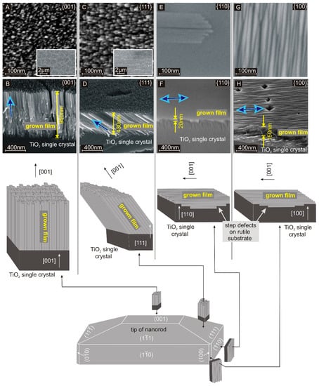
Figure 1.
Top view (A,C,E,G) and cross-section (B,D,F,H) SEM images of hydrothermally grown TiO2 structures on rutile single crystals with {001}, {111}, {110}, and {100} facets. The schematic drawing makes up a relationship between these structures and the observed facets on a common rutile TiO2 nanorod: Growth on facets perpendicular to the {001} facet is expected to be much less pronounced, which is in good agreement with the cross-section images. Growth on the {110} facet, which corresponds to the flat side walls of a nanorod results in a flat film. In contrast, growth on the {100} facet, which corresponds to the edges of a nanorod results in dense parallel gables. The principal growth direction ([001]) is marked with a blue arrow.
The hydrothermal growth on the {001} facet is shown in Figure 1A,B. On these {001} facets, the nanofingers align normal to the substrate surface, which is parallel to both the main growth direction and the [001] direction of rutile TiO2. As the nanofinger growth proceeds, the diameter decreases by approximately 5%. This is attributed to changing process parameters such as temperature and precursor concentration during the growth process [35,39]. The decrease in diameter causes cracks in the film as shown in the inset of Figure 1A. Alternatively, the nanofingers include an angle of 45° on the {111} facets, which corresponds to the angle between the [111] and [001] direction (Figure 1C,D). As demonstrated in the inset of Figure 1C, cracks are in line with the tilted growth direction since breaking up the mesocrystalline film at grain boundaries costs less energy than breaking the nanofingers directly.
The growth on {110} (Figure 1E,F) and {100} (Figure 1G,H) facets results in thin films. For the {110} facet, nanofingers are observed, which are aligned in parallel to the substrate surface. Here, the spatial growth direction along the [001] direction is perpendicular to the [110] direction. This outcome is reasonable since {110} facets form the side walls of nanorods. The thin film thickness results from a slow growth perpendicular to the main growth direction (Figure 1F). The growth on {100} facets results in a thin film with a ribbed surface. The {100} facets are found at the vertical edges of the nanorods. The ribbed surface is attributed to the growth along the face of the substrate, resulting in the edges of the nanofingers being exposed. The high density of parallel gables leads to the distinctive rough structure. Summarizing the presented observations on all four different crystal facets, we can say that the growth direction of rutile TiO2 nanocrystals is strictly correlated with the crystal orientation of the subjacent rutile TiO2 seed.
In addition to the seed crystal-dependent growth, the nanorods also exhibit branching, which results in further, uncontrolled growth directions as demonstrated in Figure 2A for {100} facets. Since the preferred growth direction on {100} facets is parallel to the surface, this phenomenon is strongly related to the branching of single rutile nanorods [35]. A similar branching event observed on a single rutile nanorod, which was created in solution without any expanded seed layer, is presented in the inset of Figure 2A. The inclination angle of 65° corresponds to the presence of a {101} twin plane at the interface between the row of nanorods and the surface of the single crystal [35]. We suppose that the branching is correlated to ruptures on {100} facets as presented in Figure 2B. If these expanded crystal defects form an intersection line with the crystal surface, a straight 1D surface defect is created. A rupture on a crystal surface provides additional exposed crystal facets with different crystallographic orientations. Such facets support branching and hence, the creation of the nanorod wall shown in Figure 2A. Yang et al. and Zhou et al. reported about similar wall-like structures grown at the side wall of a primary single freestanding TiO2 nanorod [40,41]. If surface defects on the substrates are responsible for the emergence of the observed branches, they can also be generated selectively and one can profit from the local properties of such extended nanostructures. These structures provide a bunch of important features. Twin planes between rutile nanocrystals have a stoichiometric composition that differs from defect-free TiO2. This affects the band structure at these interfaces resulting in more n- or p-type two-dimensional layers as required for thin film transistors. Beside local electronic applications, a nanocrystalline surface supports the attachment of different kinds of particles. Specific body cells are known to form a strong contact with TiO2 nanostructures and hence, these structures are suitable for applications in biological research and lab-on-a-chip devices [25]. The versatility of the applications can be significantly extended by applying a topcoat. For example, the V-shaped row of nanorods as shown in Figure 2A covered with a metallic coating serves as a waveguide for electromagnetic waves similar to the channel plasmon–polariton (CPP) geometry [42].
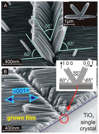
Figure 2.
(A) Scanning electron microscope (SEM) cross-section image of an extended branching site on a {100} single rutile crystal. The inset shows an individual branched nanorod, which was created in the solution in the absence of any macroscopic seed substrate. (B) SEM cross-section image of an extended branching row, where the branches were removed with sonication. The blue line marks the interface between the single-crystalline rutile TiO2 {001} substrate and the grown TiO2 layer. The red cycle marks a rupture inside the substrate that is supposed to be the origin of the branching. The principal growth direction ([001]) is marked with a blue arrow. Inset: Schematic drawing of the hydrothermal growth on {100} single crystals including a double branching event resulting in expanded nanorod walls.
4. Conclusions
We investigated the hydrothermal growth of rutile TiO2 nanocrystals on macroscopic rutile TiO2 {100}, {110}, {111}, and {001} facets. Macroscopic facets provide the growth of dense mesocrystalline rutile TiO2 films consisting of thin nanofingers. These nanofingers are aligned in parallel with the [001] direction and indicate the spatial growth direction. If the seed crystal does not exhibit a {001} facet, the spatial growth direction is tilted towards the seed surface with a well-defined angle. Thus, it is shown that the spatial growth direction is well controlled with the orientation of the employed seed crystal. Surface defects on seed crystals might support the appearance of additional spatial growth directions. Hence, an efficient control of the spatial growth direction is based on defect-free seed crystals. Nevertheless, a controlled creation of branches could be used to fabricate 2D layers with technically important electronic properties.
Supplementary Materials
The following are available online at http://www.mdpi.com/2073-4352/9/2/64/s1, Figure S1: XRD pattern of the hydrothermally grown films on the rutile single crystals., Figure S2: SEM image of rutile TiO2 nanocrystals grown on different substrates., Figure S3: SEM cross-section image of an expanded defect on a {110} single-crystalline rutile TiO2 substrate.
Author Contributions
Conceptualization, J.K. and J.A.D.; Investigation, J.K.; Data Curation, J.K. and S.S.; Writing-Original Draft Preparation, J.K.; Visualization, J.K.; Supervision, J.A.D. and L.S.-M.; Project Administration, L.S.-M.
Funding
This research was partly funded by the German Research Foundation (DFG) under the SFB1214.
Acknowledgments
We acknowledge the German Research Association (DFG), which supported the studies via the SFB1214. The presented studies are part of the project B1 and Z1 (Particle Analysis Center). Brigitte Bössenecker and Elana Harbalik supported this work as members of the Particle Analysis Center. Furthermore, J.A. Dorman thanks the Humboldt foundation for providing his research with an Alexander von Humboldt Fellowship.
Conflicts of Interest
The authors declare no conflict of interest.
References
- Liu, C.; Dasgupta, N.P.; Yang, P. Semiconductor Nanowires for Artificial Photosynthesis. Chem. Mater. 2014, 26, 415–422. [Google Scholar] [CrossRef]
- Zhou, Q.; Zhang, S.; Yang, X.; Wu, Q.; Zhao, H.; Wu, M. Rutile nanowire array electrodes for photoelectrochemical determination of organic compounds. Sens. Actuators B Chem. 2013, 186, 132–139. [Google Scholar] [CrossRef]
- Yu, X.; Han, X.; Zhao, Z.; Zhang, J.; Guo, W.; Pan, C.; Li, A.; Liu, H.; Wang, Z.L. Hierarchical TiO2 nanowire/graphite fiber photoelectrocatalysis setup powered by a wind-driven nanogenerator: A highly efficient photoelectrocatalytic device entirely based on renewable energy. Nano Energy 2015, 11, 19–27. [Google Scholar] [CrossRef]
- Liu, S.; Han, C.; Tang, Z.-R.; Xu, Y.-J. Heterostructured semiconductor nanowire arrays for artificial photosynthesis. Mater. Horiz. 2016, 3, 270–282. [Google Scholar] [CrossRef]
- Feng, X.; Zhai, J.; Jiang, L. The Fabrication and Switchable Superhydrophobicity of TiO2 Nanorod Films. Angew. Chem. Int. Ed. 2005, 44, 5115–5118. [Google Scholar] [CrossRef] [PubMed]
- Li, Y.; Sasaki, T.; Shimizu, Y.; Koshizaki, N. Hexagonal-Close-Packed, Hierarchical Amorphous TiO2 Nanocolumn Arrays: Transferability, Enhanced Photocatalytic Activity, and Superamphiphilicity without UV Irradiation. J. Am. Chem. Soc. 2008, 130, 14755–14762. [Google Scholar] [CrossRef] [PubMed]
- Chikuni, M.; Kojima, E.; Kitamura, A.; Shimohigoshi, M.; Watanabe, T. Light-induced amphiphilic surfaces. Nature 1997, 388, 431–432. [Google Scholar]
- Liu, L.; Liu, Z.; Bai, H.; Sun, D.D. Concurrent filtration and solar photocatalytic disinfection/degradation using high-performance Ag/TiO2 nanofiber membrane. Water Res. 2012, 46, 1101–1112. [Google Scholar] [CrossRef]
- Bai, H.; Liu, Z.; Liu, L.; Sun, D.D. Large-Scale Production of Hierarchical TiO2 Nanorod Spheres for Photocatalytic Elimination of Contaminants and Killing Bacteria. Chem.-Eur. J. 2013, 19, 3061–3070. [Google Scholar] [CrossRef]
- Kolmakov, A.; Moskovits, M. Chemical Sensing and Catalysis by one-dimensional Metal-Oxide Nanostructures. Annu. Rev. Mater. Res. 2004, 34, 151–180. [Google Scholar] [CrossRef]
- Francioso, L.; Taurino, A.M.; Forleo, A.; Siciliano, P. TiO2 nanowires array fabrication and gas sensing properties. Sens. Actuators B Chem. 2008, 130, 70–76. [Google Scholar] [CrossRef]
- Anitha, V.C.; Banerjee, A.N.; Joo, S.W. Recent developments in TiO2 as n- and p-type transparent semiconductors: Synthesis, modification, properties, and energy-related applications. J. Mater. Sci. 2015, 50, 7495–7536. [Google Scholar] [CrossRef]
- Sarkar, D.; Ghosh, C.K.; Mukherjee, S.; Chattopadhyay, K.K. Three Dimensional Ag2O/TiO2 Type-II (p–n) Nanoheterojunctions for Superior Photocatalytic Activity. ACS Appl. Mater. Interfaces 2013, 5, 331–337. [Google Scholar] [CrossRef] [PubMed]
- Zhang, Y.; Liu, W.; Jiang, L.; Fan, L.; Wang, C.; Hu, W.; Zhong, H.; Li, Y.; Yang, S. Template-free solution growth of highly regular, crystal orientation-ordered C60 nanorod bundles. J. Mater. Chem. 2010, 20, 953–956. [Google Scholar] [CrossRef]
- Grätzel, M. Photoelectrochemical cells. Nature 2001, 414, 338–344. [Google Scholar] [CrossRef] [PubMed]
- Enache-Pommer, E.; Boercker, J.E.; Aydil, E.S. Electron transport and recombination in polycrystalline TiO2 nanowire dye-sensitized solar cells. Appl. Phys. Lett. 2007, 91, 123116. [Google Scholar] [CrossRef]
- Liu, B.; Aydil, E.S. Growth of Oriented Single-Crystalline Rutile TiO2 Nanorods on Transparent Conducting Substrates for Dye-Sensitized Solar Cells. J. Am. Chem. Soc. 2009, 131, 3985–3990. [Google Scholar] [CrossRef]
- Yahia, S.A.A.; Hamadou, L.; Salar-García, M.J.; Kadri, A.; Ortiz-Martínez, V.M.; Hernández-Fernández, F.J.; Rios, A.P.; Benbrahim, N. TiO2 nanotubes as alternative cathode in microbial fuel cells: Effect of annealing treatment on its performance. Appl. Surface Sci. 2016, 387, 1037–1045. [Google Scholar] [CrossRef]
- Pickett, M.D.; Strukov, D.B.; Borghetti, J.L.; Yang, J.J.; Snider, G.S.; Stewart, D.R.; Williams, R.S. Switching dynamics in titanium dioxide memristive devices. J. Appl. Phys. 2009, 106, 074508. [Google Scholar] [CrossRef]
- Mujawar, S.H.; Ambade, S.B.; Battumur, T.; Ambade, R.B.; Lee, S.-H. Electropolymerization of polyaniline on titanium oxide nanotubes for supercapacitor application. Electrochim. Acta 2011, 56, 4462–4466. [Google Scholar] [CrossRef]
- Jin, J.; Huang, S.-Z.; Liu, J.; Li, Y.; Chen, L.-H.; Yu, Y.; Wang, H.-E.; Grey, C.P.; Su, B.-L. Phases Hybriding and Hierarchical Structuring of Mesoporous TiO2 Nanowire Bundles for High-Rate and High-Capacity Lithium Batteries. Adv. Sci. 2015, 2, 1500070. [Google Scholar] [CrossRef] [PubMed]
- Wen, W.; Wu, J.-M.; Jiang, Y.-Z.; Lai, L.-L.; Song, J. Pseudocapacitance-Enhanced Li-Ion Microbatteries Derived by a TiN@TiO2 Nanowire Anode. Chem 2017, 2, 404–416. [Google Scholar] [CrossRef]
- Wang, S.; Qu, D.; Jiang, Y.; Xiong, W.-S.; Sang, H.-Q.; He, R.-X.; Tai, Q.; Chen, B.; Liu, Y.; Zhao, X.-Z. Three-Dimensional Branched TiO2 Architectures in Controllable Bloom for Advanced Lithium-Ion Batteries. ACS Appl. Mater. Interfaces 2016, 8, 20040–20047. [Google Scholar] [CrossRef] [PubMed]
- Sun, Q.; Chen, K.; Liu, Y.; Li, Y.; Wei, M. Rutile TiO2 mesocrystals as a novel sulfur host for high performance lithium-sulfur batteries. Chem. Eur. J. 2017, 23, 16312. [Google Scholar] [CrossRef] [PubMed]
- Bjursten, L.M.; Rasmusson, L.; Oh, S.; Smith, G.C.; Brammer, K.S.; Jin, S. Titanium dioxide nanotubes enhance bone bonding in vivo. J. Biomed. Mater. Res. Part A 2010, 92A, 1218–1224. [Google Scholar]
- Iraj, M.; Nayeri, F.D.; Asl-Soleimani, E.; Narimani, K. Controlled growth of vertically aligned TiO2 nanorod arrays using the improved hydrothermal method and their application to dye-sensitized solar cells. J. Alloys Compd. 2016, 659, 44–50. [Google Scholar] [CrossRef]
- Wisnet, A.; Betzler, S.B.; Zucker, R.V.; Dorman, J.A.; Wagatha, P.; Matich, S.; Okunishi, E.; Schmidt-Mende, L.; Scheu, C. Model for Hydrothermal Growth of Rutile Wires and the Associated Development of Defect Structures. Cryst. Growth Design 2014, 14, 4658–4663. [Google Scholar] [CrossRef]
- Wisnet, A.; Bader, K.; Betzler, S.B.; Handloser, M.; Ehrenreich, P.; Pfadler, T.; Weickert, J.; Hartschuh, A.; Schmidt-Mende, L.; Scheu, C.; et al. Defeating Loss Mechanisms in 1D TiO2-Based Hybrid Solar Cells. Adv. Funct. Mater. 2015, 25, 2601–2608. [Google Scholar] [CrossRef]
- Chiu, F.-C. A Review on Conduction Mechanisms in Dielectric Films. Adv. Mater. Sci. Eng. 2014, 2014, 18. [Google Scholar] [CrossRef]
- Lee, J.Y.M.; Chiu, F.C.; Juan, P.C. The application of high-dielectric-constant and ferroelectric thin films in integrated circuit technology. In Handbook of Nanoceramics and Their Based Nanodevices; American Scientific Publishers: Stevenson Ranch, CA, USA, 2009; Volume 4. [Google Scholar]
- Kundu, T.K.; Lee, J.Y.-M. Thickness-Dependent Electrical Properties of Pb (Zr, Ti)O3 Thin Film Capacitors for Memory Device Applications. J. Electrochem. Soc. 2000, 147, 326–329. [Google Scholar] [CrossRef]
- Folger, A.; Kalb, J.; Schmidt-Mende, L.; Scheu, C. Fabrication and characterization of abrupt TiO2-SiOₓ core-shell nanowires by a simple heat treatment. APL Mater. 2017, 5, 086101. [Google Scholar] [CrossRef]
- Morgan, B.J.; Watson, G.W. A Density Functional Theory + U Study of Oxygen Vacancy Formation at the (110), (100), (101), and (001) Surfaces of Rutile TiO2. J. Phys. Chem. C 2009, 113, 7322–7328. [Google Scholar] [CrossRef]
- Kevane, C.J. Oxygen Vacancies and Electrical Conduction in Metal Oxides. Phys. Rev. 1964, 133, A1431–A1436. [Google Scholar] [CrossRef]
- Li, D.; Soberanis, F.; Fu, J.; Hou, W.; Wu, J.; Kisailus, D. Growth mechanism of highly branched titanium dioxide nanowires via oriented attachment. Cryst. Growth Design 2013, 13, 422–428. [Google Scholar] [CrossRef]
- Thiel, S.; Hammerl, G.; Schmehl, A.; Schneider, C.W.; Mannhart, J. Tunable Quasi-Two-Dimensional Electron Gases in Oxide Heterostructures. Science 2006, 313, 1942–1945. [Google Scholar] [CrossRef] [PubMed]
- Ando, T.; Fowler, A.B.; Stern, F. Electronic properties of two-dimensional systems. Rev. Mod. Phys. 1982, 54, 437–672. [Google Scholar] [CrossRef]
- Keyser, U.F.; Schumacher, H.W.; Zeitler, U.; Haug, R.J.; Eberl, K. Fabrication of a single-electron transistor by current-controlled local oxidation of a two-dimensional electron system. Appl. Phys. Lett. 2000, 76, 457–459. [Google Scholar] [CrossRef]
- Kalb, J.; Dorman, J.A.; Folger, A.; Gerigk, M.; Knittel, V.; Plüisch, C.S.; Trepka, B.; Lehr, D.; Chua, E.; Goodge, B.H.; et al. nfluence of substrates and rutile seed layers on the assembly of hydrothermally grown rutile TiO2 nanorod arrays. J. Cryst. Growth 2018, 494, 26–35. [Google Scholar] [CrossRef]
- Yang, X.; Jin, C.; Liang, C.; Chen, D.; Wu, M.; Yu, J.C. Nanoflower arrays of rutile TiO2. Chem. Commun. 2011, 47, 1184–1186. [Google Scholar] [CrossRef]
- Zhou, W.; Liu, X.; Cui, J.; Liu, D.; Li, J.; Jiang, H.; Wang, J.; Liu, H. Control synthesis of rutile TiO2 microspheres, nanoflowers, nanotrees and nanobelts via acid-hydrothermal method and their optical properties. CrystEngComm 2011, 13, 4557–4563. [Google Scholar] [CrossRef]
- Bozhevolnyi, S.I.; Volkov, V.S.; Devaux, E.; Laluet, J.-Y.; Ebbesen, T.W. Channel plasmon subwavelength waveguide components including interferometers and ring resonators. Nature 2006, 440, 508. [Google Scholar] [CrossRef] [PubMed]


© 2019 by the authors. Licensee MDPI, Basel, Switzerland. This article is an open access article distributed under the terms and conditions of the Creative Commons Attribution (CC BY) license (http://creativecommons.org/licenses/by/4.0/).