Abstract
We report on the role of AlSb material in the reduction of threading dislocation density (TDD) in the GaSb/AlSb/GaAs system. The AlSb layers were grown using low-temperature (LT) MBE, exploiting the interfacial misfit (IMF) dislocation array. AlSb layers with four different thicknesses in the range of 1–30 nm were investigated. The results showed the inhibiting role of LT-AlSb layers in the reduction of TDD. Values of TDD as low as 2.2 × 10⁶ and 6.3 × 106 cm−2 for samples with thin and thick AlSb layers were obtained, respectively. The filtering role of AlSb material was proven despite the IMF-AlSb/GaAs interface’s imperfectness caused by the disturbance of a 90° dislocation periodic array by, most likely, 60° dislocations. The dislocation lines confined to the region of AlSb material were visible in HRTEM images. The highest crystal quality and smoother surface of 1.0 μm GaSb material were obtained using 9 nm thick AlSb interlayer. Unexpectedly, the comparative analysis of the results obtained for the GaSb/LT-AlSb/GaAs heterostructure and our best results for the GaSb/GaAs system showed that the latter can achieve both higher crystal quality and lower dislocation density.
1. Introduction
Gallium arsenide has many well-documented advantages, which make it the most commonly used substrate in the optoelectronic devices operating in the near-infrared spectral range [1,2,3]. However, there is an issue of the lattice mismatch between GaAs and antimonide-based compounds used more and more in mid-infrared technology. For instance, the lattice constants of GaAs and GaSb differ by 7.8%. The strain energy is released by generation of 60° misfit dislocations. About 1010 cm−2 dislocations are necessary to completely relax the lattice in a GaSb/GaAs system [4]. There are two most commonly used approaches to reduce the dislocation density; namely, growth of the metamorphic material [5] and interfacial misfit dislocation (IMF) arrays [6]. The first one requires deposition of thick layer [7,8], whereas the second one offers almost full strain relaxation within few monolayers of the material [9]. The lowest threading dislocation density (TDD) of 5 × 105 cm−2 (7 × 105 cm−2), estimated from the plan-view TEM images (based on the etching and counting of the pits on the surface), was obtained for the GaSb/GaAs system by Huang et al. [9,10]. To the best of our knowledge this result has not been repeated. Despite many years of development, the performances of the structures grown on the IMF-GaSb-buffered GaAs substrates are lower than those grown on the native substrates [11,12,13,14]. This justifies renewed efforts of many research groups to optimize this relaxation mode either by optimizing the growth conditions [15,16] or by applying an additional buffer in a GaSb/GaAs system [17,18,19,20,21]. The latter approach has shown significant promise. Zhou et al. [17] obtained high crystal quality of GaSb layer grown on GaAs by optimizing the growth temperature and the thickness of AlSb interlayer. They got the best results for 450 °C and 2.1 nm-thick AlSb buffer. Hao et al. [18] demonstrated stronger photoluminescence intensity from GaSb layer deposited on AlSb/GaSb SL buffer as evidence of higher GaSb material quality. Wang et al. proved that Sb-soaking of GaAs surface prior to the AlSb deposition resulted in a narrow interface of 0.7 nm and low dislocation density of 6 × 107 cm−2 compared to 8 × 108 cm−2 obtained without AlSb [19]. It was also shown that LT-MBE grown AlSb islands with nominal thicknesses of 1.2 nm ensured strain relaxation by the generation of periodic array of 90° dislocations, similarly to the findings for GaSb buffer [20]. The reduction of the threading dislocation density was visualized in TEM images, but no reference to the quantitative analysis was given. The influences of the growth temperature and the distance of the AlSb layer from the GaSb/GaAs interface on TDD were investigated by Mansoori et al. [21]. The authors concluded that both low-temperature growth at 420 °C and 250 nm distance promoted the reduction of threading dislocations. They obtained an about four times lower TDD of 4 × 107 cm−2 for the GaSb/AlSb/GaSb/GaAs system than the 1.5 × 108 cm−2 TDD for GaSb/GaAs.
The aforementioned information does not provide an explanation of the role the AlSb layer plays in the process of TDD reduction in GaSb/LT-AlSb/GaAs system. The main focus of this paper is to report new results supporting the positive role of LT-AlSb in decreasing TDD. Both thin and thick AlSb layers grown using low-temperature (LT) technology were taken under consideration. The thinnest layers had thicknesses comparable to the critical value determined from Matthews–Blakesly formula under the assumption of 2D growth modes [22], whereas the thickest to the multiple of the island coalescence limit determined by Ripalda et al. [23]. The results proved the role of both LT-AlSb layers in the process of TDD reduction. The values of TDD of 2.2 × 106 cm−2 and 6.3 × 106 cm−2 were obtained for GaSb/LT-AlSb/GaAs heterostructures with thin and thick AlSb layers, respectively. The AlSb filtering role was observed despite some imperfectness revealed at the IMF-AlSb/GaAs interface. HRTEM images disclosed the dislocation lines confined to the region of AlSb layer. The comparative analysis of the results obtained for GaSb/LT-AlSb/GaAs and GaSb/GaSb material systems showed that both higher crystal quality and lower dislocation density could be obtained for the latter.
The paper is divided into two main sections. Section 2 is devoted to describing the experiment. In Section 3, the results obtained for the GaSb/GaAs system deposited without (Section 3.1) and with an AlSb interlayer (Section 3.2) are presented.
2. Experiment
The aim of the experiment was to check how the reduction of TDD in the GaSb/AlSb/GaAs material system is influenced by the growth conditions and thickness of the AlSb layer. Four types of the heterostructures, shown in Figure 1, were deposited.
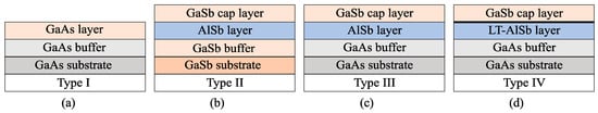
Figure 1.
Schematic diagrams of the structures investigated: #554 and #629 (a); #642 (b); #643 (c); and #646, #647, #648, #650 and #651 (d). The bold line in the last diagram (d) indicates the interface between LT-AlSb layer and GaSb layer.
Before the beginning of the experiment, reference samples were prepared. Firstly, IMF-GaSb layers on GaAs substrates were grown under optimal (type I, #629) and non-optimal (type I, #554) IMF conditions to highlight the best result [8,24]. Secondly, AlSb growth conditions (type II, #642) and the application of the AlSb material as a buffer layer (type III, #643) were also verified. Finally, samples #646, #647, #648, #650 and #651 were grown according to scheme IV. The low-temperature AlSb layers with different thicknesses were examined.
The Si-doped GaAs and undoped GaSb substrates were used. A two-hundred-and-fifty-nanometer-thick smoothing layer was deposited. GaSb and AlSb layers had thicknesses dL of at least 500 nm. The LT-AlSb layer thickness dAlSb was different for each sample, but did not exceed 30 nm. A five-nanometer-thick GaSb cap layer was deposited on top of AlSb material to prevent oxidation. Heterostructures were grown using molecular beam epitaxy (MBE) in RIBER 32P machine. The reactor was equipped with the classical effusion cell for Al, the SUMO cell for Ga and the valved cracker As and Sb cells. The in-situ monitoring of the growth process was carried out using the reflection high-energy electron diffraction (RHEED) method. The temperature was measured using the IRCON pyrometer (spectral response peak at 930 nm, 450–1200 °C) and controlled through the oxide desorption and the RHEED oscillations at temperatures below 500 °C for GaAs and GaSb materials, respectively. The growth rate was about 1.0 Å/s and 1.5 Å/s for GaAs, and GaSb and AlSb, respectively. The growth temperature was about 580 °C for GaAs and 520 °C for GaSb. The ratios of the beam equivalent pressure of group V to group III elements, henceforth V/III, were 8.0 and 3.5 for GaAs and GaSb, respectively. The growth parameters are collected in Table 1.

Table 1.
The growth parameters of the investigated structures. Labels: dL—layer thickness, TAlSb—AlSb growth temperature, tAs = 0—time of As-pressure reduction, tSb—Sb-soaking time, V/III—ratio of beam equivalent pressure of group V to group III elements and dLT—LT-AlSb thickness.
The growth stages for structures deposited on GaAs substrate were as follows. The substrates were heated to desorb the oxide and annealed as described in [24]. Then the substrate was cooled down to the growth temperature of the buffer layer (580 °C and 520 °C for GaAs and GaSb, respectively) and then the growth was initiated. The RHEED pattern of (2 × 4) was observed during the GaAs growth and was (1 × 3) for the GaSb buffer. After the growth termination by Ga-flux interruption, the temperature was decreased to TAlSb under As-surface stabilization. Prior to Sb-soaking of GaAs surface for tSb, As-flux was interrupted for tAs = 0 and then the AlSb growth was started by opening the Al cell. The growth of GaSb material on the AlSb layer (type II, III and IV) or AlSb on the GaSb layer (type II) was initiated by simultaneous closing the Al cell and opening the Ga cell. The type I structure is a simpler version of the type IV one—the stage described for AlSb refers to the GaSb layer. The cap layer was not deposited in type I structure. During the growth of the LT-AlSb layer, some observations were made based on the RHEED patterns. For the first 3.0 s (the nominal AlSb thickness of 1.5 ML) the RHEED pattern was (2 × 8). Next, the RHEED pattern changed to the spotty one and lasted for 7.0 s, during which the formation of the islands occurred (~3.5 MLs) and was followed by (1 × 3) reconstruction. The transition between the growth of AlSb and GaSb took place without any changes in the RHEED pattern; i.e., (1 × 3) reconstruction was maintained.
The samples were characterized using atomic force microscopy (AFM), scanning electron microscopy (SEM), high-resolution X-ray diffraction (HRXRD) and high-resolution transmission electron microscopy (HRTEM).
3. Results and Discussion
Four basic material parameters describing the samples, such as surface roughness, TDD, crystal quality (intensity and full width at half maximum of rocking curve) and ΔqZ/ΔqX ratio were monitored. The ΔqZ/ΔqX ratio defined by Kaganer et al. indicates the type of the dislocation taking part in the strain relaxation process [25]. The authors showed that the ΔqZ/ΔqX can be described as: for 90° dislocations and for 60° dislocations, where is Poisson’s ratio. The ΔqZ/ΔqX values were calculated for both 90° and 60° dislocations for GaSb and AlSb materials (Table 2). Intermediate values suggest the presence of both and/or mixed type dislocations.
Table 2.
ΔqZ/ΔqX ratios calculated for the 90° and 60° dislocations in GaSb and AlSb. Labels: c11, c12 [1011 dyn/cm2]—elastic constants [26].
Additionally, in [23] it was pointed out that the experimental values of ΔqZ/ΔqX can be obtained from , where wz and wx are FWHM values of intensity distribution at 004 reciprocal lattice point in qz and qx directions, respectively.
The structural parameters are collected in Table 3. The two-dimensional (2D) growth mode was observed (AFM) for all samples investigated except one (Figure 2). The flowing terraces were visible on the surface of the samples deposited on the native substrate (#642, Figure 2c). The spiral growth was characteristic for the GaSb grown on GaAs substrate (for example #629 and #647, Figure 2b,d). Thick 5.0 µm-GaSb layer (#554) on GaAs substrate without AlSb layer was an exception (Figure 2a).
Table 3.
Structural parameters for the samples investigated. Labels: TDD—threading dislocation density, RMS—root mean square, EPD—etch pit density, I—rocking curve intensity of GaSb peak, FWHM—full width at half maximum of I and ΔqZ/ΔqX—parameter determined from reciprocal space map measured around symmetrical 004 GaSb reciprocal lattice point.
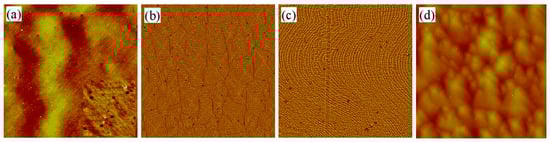
Figure 2.
The 10 × 10 µm AFM top view (a,d) and differential (b,c) images of GaSb surfaces grown in 3D (b,d) and 2D (a,c) mode for #554 (a), #629 (b), #642 (c) and #647 (d) samples. 0.5 × 0.5 µm inset in (a) shows 2.5 nm-deep holes with density of 5.8 × 109 cm−2.
The two-dimensional spiral growth made it possible for us to determine the dislocation density because the pyramids visible on the GaSb surface formed around the screw dislocations [27,28]. The absolute majority of threading dislocations in GaSb material were of mixed type; i.e., with the screw component of the Burger vector [29]. Thus, if a single pyramid corresponded to only a single dislocation, the pyramids density would be equal to the TDD. However, one can see that for all samples, the TDDs determined from AFM images were higher than the dislocation densities estimated by counting the etch pits (EPD) (Table 3). The sizes of both the smallest pyramids and the smallest etch pits visible on the comparable area of the sample surface (10 × 10 µm-AFM image, 8.5 µm × 8.5 µm-SEM image) were similar to each other. The smallest length of the pyramid base and the elongated dimension of the pit were about 0.25 µm and 0.33 µm, respectively. Thus, the size of the pits and the pyramids cannot be the reason of this discrepancy. Taking into account that some pyramids can be formed without participation of the screw dislocations [27], it should be assumed that the values determined from AFM observations might be overestimated.
Good crystal quality of all samples grown with LT-AlSb interlayer was proven by relatively small FWHM of HRXRD peaks. In similar investigations, Zhou Z.-Q. et al. obtained FHWM of 348 arcsec for an AlSb thickness of 2.1 nm and GaSb thickness of 500 nm [17]. A little bit wider of a peak in [17] could be caused by a thinner GaSb layer.
3.1. The Growth Preceding Investigation of the LT-AlSb Interlayer
The five-micrometer-thick GaSb layer (#554) grown on GaAs substrate was analyzed to emphasize the achievement of optimal IMF-GaSb/GaAs growth (#629). Furthermore, it was shown that 2D step-flow mode is possible in this material system. The GaSb surface with narrow, straight and parallel terraces of 1 ML step height was formed. Round, 2.5 nm-deep holes were observed (inset in Figure 2a), which was not the case for other samples. The hole density of 5.8 × 109 cm−2 was about three orders of magnitude higher than the dislocation density. The origin of these holes is unclear. Their depth suggests that they could be created during the sample cooling after the growth termination. However, this stage was the same for all samples, which excludes it as a potential cause. The TDD of 7.8 × 106 cm−2 determined by counting of the etched pits was unexpectedly high, especially taking into account that it was obtained for the 5.0 µm-thick sample. It can be expected that in such a large volume of material some dislocations will be annihilated. Others could bend and propagate to the edge of the sample, which should result in lower threading dislocation density compared to the value obtained for thinner layer (#629, EPD = 3.5 × 106 cm−2). The crystal quality defined as the intensity and FWHM of the rocking curve can be evaluated by comparing the samples with similar thicknesses. Based on the results obtained for 5.0 µm-thick GaSb layer in previous studies (#39B, IRC = 4.4 × 10⁶ cts, FWHMRC = 125 arcsec [24]), we can state that high TDD only slightly disturbed the crystal quality of sample #554. A low value of the ΔqZ/ΔqX ratio equal to 0.53 indicates that mixed type dislocations (60°) or mixed dislocations (60°, 90°) were formed during the lattice relaxation of this sample. This increases the probability of the value of TDD obtained being correct. The interface shown in TEM images seems to be strained (Figure 3). Both TEM cross-section (Figure 3a) and HRTEM images (Figure 3b,c) show wavy forms, which suggest that the lattice is strained. However, the symmetrical and asymmetrical reciprocal space maps (RSMs, not shown) did not corroborate this. On the contrary, high lattice relaxation of 99.8% was determined. We believe that almost complete relaxation was achieved by both mixed type misfit dislocations at the interface and randomly generated threading dislocations in the material volume. The reason behind the wavy interface may also be related to very low thickness of the sample prepared for TEM observations. Very thin specimen made of highly lattice-mismatched material can locally bend. This bending can be seen in the high resolution images even at lower magnifications. No correspondence between the amplitude of the wavy structure at the interface and 2.5 nm-deep holes visible in AFM image (Figure 2a) was found.
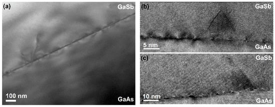
Figure 3.
TEM images obtained for #554 GaSb/GaAs structure: the cross section (a); HRTEM images of GaSb/GaAs interface with linear defects (b,c).
For sample #629, the ΔqZ/ΔqX ratio was 0.63 (Figure 4a), and mainly 90° dislocations were generated at the GaSb/GaAs interface. This contributed to more than two times lower threading dislocation density (EPD = 3.5 × 106 cm−2) obtained for five times thinner buffer in comparison with the previous sample. This proves the superiority of the short-time As-pressure reduction (#629, tAs = 3.0 s) over the long one (#554, tAs = 200 s). In further investigations the tAs of 10.0 s was used.
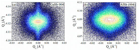
Figure 4.
The symmetrical 004 reciprocal space maps obtained for #629 GaSb/GaAs with ΔqZ/ΔqX of 0.63 and the relaxation of 99.7% (a) and #643 AlSb/GaAs with ΔqZ/ΔqX of 0.70 and the relaxation of 97.7% (b).
Thick AlSb layers were grown before the beginning of the investigation of LT-AlSb layers used for the reduction of the misfit dislocation density at GaSb/GaAs interface. The #642 type II and #643 type III samples were deposited to verify the growth parameters and check the application of AlSb material as a buffer layer, respectively. The one-monolayer-smooth surface with 2D flowing terraces of AlSb layer deposited on the native substrate (#642) proved that the growth conditions were optimal. Partial relaxation of 61.5% and the ΔqZ/ΔqX ratio of 0.65 were determined based on both symmetrical and asymmetrical reciprocal space maps (not shown). This value of ΔqZ/ΔqX indicates that the relaxation occurred by the generation of the mixed type misfit dislocations as the theoretical value for 90° dislocations in AlSb material is 0.70 (Table 1). TDD was not estimated successfully despite the fact that many attempts were made. The AFM approach was useless for step-by-step growth. No etch pits were revealed using well-known chemical solutions for the bulk AlSb material (HCl:HNO3 = 1:1, HCl:H3PO4 = 1:4, HCl, (FeCl3:H2O = 1:50):(HCl:H2O = 1:1), H2O:HCl:HNO3 = 10:1:1). Sample #643 (AlSb/GaAs heterostructure) also had an atomically smooth surface; however, the spiral growth mode was observed instead of flowing terraces. The threading dislocation density of 1.64 × 108 cm−2 was determined based on the AFM images. The ΔqZ/ΔqX ratio of 0.70 indicated that only edge dislocations were involved in the lattice relaxation (97.7%), determined from symmetrical (Figure 4b) and asymmetrical (not shown) RSMs. Very high TDD and substantial residual strain in the material ipso facto disqualified thick AlSb as a buffer layer even though ΔqZ/ΔqX ratio was close to the theoretical limit. In the following subsections, the results of the applicability tests of LT-AlSb layer in the reduction of dislocation density are presented (please refer to Figure 1d).
3.2. The Investigations with LT-AlSb Layer
Two-dimensional spiral growth was observed on the surface of the type IV samples. The surface roughness was smaller than 2.0 nm on average. TDD determined based on the AFM images was ~107 cm−2, under the assumption that each pyramid grew around single mixed type dislocation. TDD is above one order of magnitude higher than EPD (~106 cm−2) for all GaSb/AlSb/GaAs samples, except the one with 2.0 nm-thick AlSb layer grown at V/III = 2.0 (#646). Dislocations on the (100) GaSb surface were revealed by etching in a FeCl3:HCl-based solution after chemical degreasing in the acetone and isopropanol. The example of the etch pits revealed on sample #647 surface is shown in Figure 5.
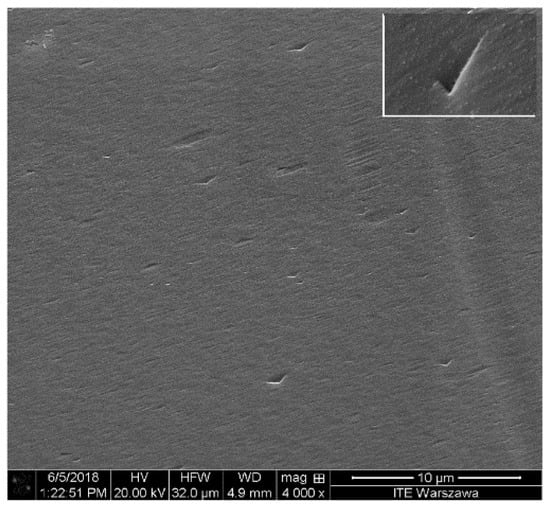
Figure 5.
SEM images obtained for sample #647. The inset shows the shape of the etched pit corresponding to the threading dislocation. EPDav is 6.3 × 106 cm−2.
Although there was no clear correlation between the dislocation density and the crystal quality of GaSb layer, the samples were divided into to two groups based on the share of 90° dislocations in the relaxation process: set I with ΔqZ/ΔqX ratio below 0.60 and set II with ΔqZ/ΔqX ratio of at least 0.62. The first group consisted of two samples with the AlSb thickness below the island coalescence threshold (#646 and #650). The two-nanometer-thick AlSb layer was used as a datum point in the experiment. We believe that 2.0 nm-AlSb layer was fully relaxed and did not introduce additional stress into the GaSb layer grown on top of it. Sample #650 grown at higher V/III ratio of 3.2 for AlSb layer showed a larger ΔqZ/ΔqX value of 0.59 and narrower peak of the rocking curve than sample #646 deposited at lower V/III ratio of 2.0. This indicated a higher density of 90° dislocations at the GaAs/AlSb interface, which could justify lower dislocation density in #650-GaSb material. This is more consistent with EPD than AFM estimations (Table 3). A relatively large difference between FWHMRC of both analyzed samples (ΔFWHMRC = 20 arcsec) could explain the two times higher dislocation density determined from EPD for sample #646. The second set contained samples with well-defined interfaces of AlSb layers. The ΔqZ/ΔqX ratio was larger than or equal to 0.62, which indicated the majority share of 90° dislocations in the lattice relaxation. Sample #651 with the thinnest AlSb layer of 1.0 nm was grown using two times longer Sb-soaking time (10.0 s) prior to the initiation of AlSb growth compared to the other samples. We assumed that it would increase the chemical uniformity of the bottom AlSb interface. The sharper the interface, the higher the crystal quality of the IMF material. The improvement of the crystal quality was observed in comparison with set I, but the parameters were still below those obtained for the best GaSb/GaAs structure (#629, Table 3). A fully strained AlSb layer introduced an additional interface into the GaSb/GaAs structure. It acted as a filter impeding the movement of the dislocation lines. Strong reduction of dislocation density was observed, especially if EPD values were to be considered (2.2 × 106 cm−2). The thickest AlSb layer worsened the crystal quality of GaSb material (#648) in comparison with the previously analyzed sample #651, even though, it was significantly thinner than the limit of the accumulation of own compressive strain determined by Ripalda et al. [23] (42.0 nm). Nevertheless, the filtering role of AlSb was maintained. The EPD value was low (3.0 × 106 cm−2) and comparable with the best result of 3.5 × 106 cm−2 obtained by us for IMF-GaSb/GaAs structure without AlSb layer.
The last analyzed GaSb/AlSb/GaAs structure (#647) was grown with the intermediate value of AlSb layer thickness of 9.0 nm. It guaranteed the termination of the island coalescence and the complete relaxation of AlSb material. According to Ripalda et al. [23], it allows one to avoid the undulations at the interface and the worsening of the crystal quality. Recently, Korkmaz et al. successfully applied an LT-AlSb interlayer with a similar thickness as in sample #647, in the growth of mid-infrared photodiodes [30]. TEM cross-sectional image for the sample was compared with the one obtained for the best GaSb/GaAs sample (#629) grown without AlSb layer, Figure 6. The lack of undulations at the interface region can be seen. A larger number of threading dislocations propagated over the GaSb material grown on AlSb layer, but almost all of them stopped in the middle of GaSb layer. The inset in Figure 6b presents the evidence for the filtering role of AlSb layer. The dislocation lines terminated at the upper AlSb interface and their further propagation was not observed. The ΔqZ/ΔqX ratio reached 0.64, which is the theoretical limit for GaSb/GaAs system (Table 2). This indicated that the lattice strain was relaxed by the generation of only 90° dislocations. The HRTEM images of samples #629 and #647 are shown in Figure 7. The regular array of misfit dislocations at the interfaces of both samples can be seen. Every 14th atomic plane was skipped in GaAs material. The average distance between dislocations was 5.56 nm and 5.46 nm for #629 and #647 structures, respectively. Further analysis showed that the Burger vectors for misfit dislocations pointed in the same direction and were located in the interface plane. However, for 5th, 6th and 7th loops in Figure 6b, there was more than one dislocation present within each loop. The enlarged area around these dislocations is shown in Figure 8.
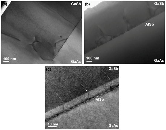
Figure 6.
TEM cross-sectional images obtained for structures: #629 GaSb/GaAs (a) and #647 GaSb/AlSb/GaAs (b,c). The filtering role of the AlSb layer is shown in (c). The white arrows indicate threading dislocations terminated at the AlSb/GaSb interface.
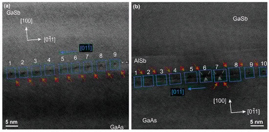
Figure 7.
HRTEM images obtained for structures: #629 with the periodic array of 90° dislocations (a) and #647 GaSb/GaAs with branches of the 60° dislocations (b).
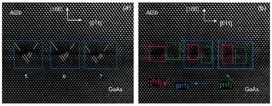
Figure 8.
HRTEM images obtained for #647 GaSb/AlSb/GaAs structure in the area of 5th, 6th and 7th dislocation at the interface AlSb/GaAs show the lattice imperfections: skipped atomic planes in GaAs shifted by three atomic planes (a) and the Burger’s loop analysis (b).
In the case of 90° dislocations, it is possible to select two atomic planes of GaAs going into one atomic plane of GaSb for the diagonal atomic planes of GaAs (not parallel to the interface). The intersection point is located within the dislocation in the interface plane. This situation took place for all dislocations labelled in Figure 6 except for 5th, 6th and 7th ones. For the latter, the skipped GaAs atomic planes were shifted by 3 MLs (Figure 8a), which allowed for the existence of two dislocations very close to each other. The detailed loop analysis of these dislocations (Figure 8b) showed that they had different, [−11−1] and [11−1], Burger’s vectors. Their sum gives a [01−1] vector, which corresponds to the observed 90° dislocations. These additional dislocations detected at the AlSb/GaAs interface could be responsible for the higher TDD in GaSb/LT-AlSb/GaAs structure. Similar and other lattice imperfections were also reported by Wang et al. [19]. The authors observed them at the GaSb/GaAs interface.
4. Conclusions
The role of AlSb interlayers with different thicknesses in TDD reduction was investigated. The experiment was divided into two stages. Firstly, bulk AlSb layers on GaSb and GaAs substrates were grown to verify the conditions and the application of bulk AlSb material as a buffer layer. Secondly, the impact of thin AlSb interlayer deposited at a low temperature on the dislocation array was examined. Very high TDD and residual strain disqualified thick AlSb as a buffer layer. Values of TDD as low as 2.2 × 106 cm−2 and 6.3 × 106 cm−2 were obtained for GaSb/LT-AlSb/GaAs heterostructures with 1.0 nm and 9.0 nm AlSb layers, respectively. Higher crystal quality and a smoother surface of IMF-GaSb material were obtained for the thicker AlSb interlayer. The filtering role of AlSb layer was proven. HRTEM images showed that the dislocation lines are confined to the region of AlSb material. Despite the filtering role of AlSb, a two-times higher TDD was observed for the sample #647 in comparison to the sample #629 without AlSb layer. TDD affected the overall crystal quality of the GaSb material in the sample #647, which manifested as a little bit of a smaller and wider peak of the rocking curve. Some imperfections detected at the AlSb/GaAs interface could be responsible for the higher TDD in the GaSb/LT-AlSb/GaAs structure; namely, the 90° dislocation periodic array was disturbed by most likely 60° dislocations.
Author Contributions
Conceptualization, A.J.; methodology, A.J.; validation, A.J., K.C. and I.S.; formal analysis, A.J.; investigation, A.J., J.R., I.S., A.W. and D.S.; resources, A.J.; data curation, K.C.; writing—original draft preparation, A.J.; writing—review and editing, K.C., A.J. and I.S., A.W.; visualization, I.S. and K.C.; supervision, A.J.; project administration, A.J.; funding acquisition, A.J.
Funding
This research was partially funded by the National Science Centre (NCN), project number 2013/11/B/ST7/04341, and by the National Centre for Research and Development (NCBR), project number TECHMATSTRATEG1/347751/5/NCBR/2017.
Acknowledgments
The authors would like to thank K. Regiński for his support and assistance with these projects.
Conflicts of Interest
The authors declare no conflict of interest.
References
- Yamaguchi, M.; Takamoto, T.; Araki, K.; Ekins-Daukes, N. Multi-junction III-V solar cells: current status and future potential. Sol. Energy 2005, 75, 78–85. [Google Scholar] [CrossRef]
- Czyszanowski, T.; Sarzała, R.P.; Dems, M.; Nakwaski, W.; Thienpont, H.; Panajotov, K. Optimal photonic-crystal parameters assuring single-mode operation of 1300 nm AlInGaAs vertical-cavity surface-emitting laser. J. Appl. Phys. 2009, 105, 093102. [Google Scholar] [CrossRef]
- Jasik, A.; Sokol, A.K.; Broda, A.; Sankowska, I.; Wojcik-Jedlinska, A.; Wasiak, M.; Kubacka-Traczyk, J.; Muszalski, J. Dual-wavelength vertical external-cavity surface-emitting laser: strict growth control and scalable design. Appl. Phys. B 2016, 122, 23. [Google Scholar] [CrossRef]
- Kyutt, R.N.; Scholz, R.; Ruvimov, S.S.; Argunova, T.S.; Budza, A.A.; Ivanov, S.V.; Kopev, P.S.; Sorokin, L.M.; Scheglov, M.P. Dislocation structure of epitaxial GaSb films grown on (001) GaAs substrates by molecular beam epitaxy. Phys. Solid State 1993, 35, 372–378. [Google Scholar]
- Chen, X.Y.; Gu, Y.; Zhang, Y.G.; Ma, Y.J.; Du, B.; Zhang, J.; Ji, W.Y.; Shi, Y.H.; Zhu, Y. Growth temperature optimization of GaAs-based In0.83Ga0.17As on InxAl1−xAs buffers. J. Cryst. Growth 2018, 488, 51–56. [Google Scholar] [CrossRef]
- Rocher, A.M. Interfacial dislocations in the GaSb/GaAs (001) heterostructure. Solid State Phenom. 1991, 19, 563–572. [Google Scholar] [CrossRef]
- Song, Y.; Kujofsa, T.; Ayers, J.E. Threading dislocations in InGaAs/GaAs (001) buffer layers for metamorphic high electron mobility transistors. J. Electron. Mater. 2018, 47, 3474–3482. [Google Scholar] [CrossRef]
- Jasik, A.; Sankowska, I.; Ratajczak, J.; Wawro, A.; Smoczyński, D.; Czuba, K.; Wzorek, M. Atomically smooth interfaces of type-II InAs/GaSb superlattice on metamorphic GaSb buffer grown in 2D mode on GaAs substrate using MBE. Current Appl. Phys. 2019, 19, 120–127. [Google Scholar] [CrossRef]
- Huang, S.H.; Balakrishnan, G.; Khoshahklagh, A.; Jallipalli, A.; Dawson, L.R.; Huffaker, D.L. Strain relief by periodic misfit arrays for low defect density GaSb on GaAs. Appl. Phys. Lett. 2006, 88, 131911. [Google Scholar] [CrossRef]
- Huang, S.; Balakrishnan, G.; Huffaker, D.L. Interfacial misfit array formation for GaSb growth on GaAs. J. Appl. Phys. 2009, 105, 103104. [Google Scholar] [CrossRef]
- Craig, A.P.; Marshall, A.R.J.; Tian, Z.-B.; Krishna, S. Mid-infrared InAsSb-based nBn photodetectors with AlGaAsSb barrier layers–Grown on GaAs, using an interfacial misfit array, and on native GaSb. Infrared Phys. Technol. 2014, 67, 210–213. [Google Scholar] [CrossRef]
- Ahirwar, P.; Shima, D.; Rotter, T.J.; Clark, S.P.R.; Addamane, S.J.; Hains, C.P.; Dawson, L.R.; Balakrishnan, G.; Bedford, R.; Lai, Y.Y.; et al. TEM based analysis of III-Sb VECSELs on GaAs substrates for improved laser performance. In Proceedings of the SPIE 8606, Vertical External Cavity Surface Emitting Lasers (VECSELs) III, San Francisco, CA, USA, 26 February 2013; Volume 8606. [Google Scholar] [CrossRef]
- Nguyen, B.-M.; Hoffman, D.; Huang, E.K.-W.; Bogdanov, S.; Delaunay, P.-Y.; Razeghi, M.; Tidrow, M.Z. Demonstration of mid infrared type-II InAs/GaSb superlattice photodiodes grown on GaAs substrate. Appl. Phys. Lett. 2009, 94, 223506. [Google Scholar] [CrossRef]
- Juang, B.-C.; Laghumavarapu, R.B.; Foggo, B.J.; Simmonds, P.J.; Lin, A.; Liang, B.; Huffaker, D.L. GaSb thermophotovoltaic cells grown on GaAs by molecular beam epitaxy using interfacial misfit arrays. Appl. Phys. Lett. 2015, 106, 111101. [Google Scholar] [CrossRef]
- Richardson, C.J.K.; He, L.; Kanakaraju, S. Metamorphic growth of III-V semiconductor bicrystals. J. Vac. Sci. Technol. B 2011, 29, 03C126. [Google Scholar] [CrossRef]
- Reyner, C.J.; Wang, J.; Nunna, K.; Lin, A.; Liang, B.; Goorsky, M.S.; Huffaker, D.L. Characterization of GaSb/GaAs interfacial misfit arrays using x-ray diffraction. Appl. Phys. Lett. 2011, 99, 231906. [Google Scholar] [CrossRef]
- Zhou, Z.-Q.; Xu, Y.-Q.; Hao, R.-T.; Tang, B.; Ren, Z.-W.; Niu, Z.-C. Molecular Beam Epitaxy of GaSb on GaAs Substrates with AlSb Buffer Layers. Chin. Phys. Lett. 2017, 26, 018101. [Google Scholar]
- Hao, R.; Deng, S.; Shen, L.; Yang, P.; Tu, J.; Liao, H.; Xu, Y.; Niu, Z. Molecular beam epitaxy of GaSb on GaAs substrates with AlSb/GaSb compound buffer layers. Thin Solid Films 2010, 519, 228–230. [Google Scholar] [CrossRef]
- Wang, Y.; Ruterana, P.; Desplanque, L.; Kazzi, S.El.; Wallart, X. Strain relief at the GaSb/GaAs interface versus substrate surface treatment and AlSb interlayers thickness. J. Appl. Phys. 2011, 109, 023509. [Google Scholar] [CrossRef]
- Kim, H.S.; Noh, Y.K.; Kim, M.D.; Kwon, Y.J.; Oh, J.E.; Kim, Y.H.; Lee, J.Y.; Kim, S.G.; Chung, K.S. Dependence of the AlSb buffers on GaSb/GaAs(001) heterostructures. J. Cryst. Growth 2007, 301, 230–234. [Google Scholar] [CrossRef]
- Mansoori, A.; Addamane, S.J.; Renteria, E.J.; Shima, D.M.; Behzadirad, M.; Vadiee, E.; Honsberg, C.; Balakrishnan, G. Reducing threading dislocation density in GaSb photovoltaic devices on GaAs by using AlSb dislocation filtering layers. Sol. Energy Mater. Sol. Cells 2018, 185, 21–27. [Google Scholar] [CrossRef]
- Matthews, J.W.; Blakeslee, A.E. Defects in epitaxial multilayers: I. Misfit dislocations, J. Cryst. Growth 1974, 27, 118–125. [Google Scholar] [CrossRef]
- Ripalda, J.M.; Sanchez, A.M.; Taboada, A.G.; Rivera, A.; Alén, B.; González, Y.; González, L.; Briones, F.; Rotter, T.J.; Balakrishnan, G. Relaxation dynamics and residual strain in metamorphic AlSb on GaAs. Appl. Phys. Lett. 2012, 100, 012103. [Google Scholar] [CrossRef]
- Jasik, A.; Sankowska, I.; Wawro, A.; Ratajczak, J.; Jakieła, R.; Pierścińska, D.; Smoczyński, D.; Czuba, K.; Regiński, K. Comprehensive investigation of the interfacial misfit array formation in GaSb/GaAs material system. Appl. Phys. A 2018, 124, 512. [Google Scholar] [CrossRef]
- Kaganer, V.M.; Köhler, R.; Schmidbauer, M.; Opitz, R.; Jenichen, B. X-ray diffraction peaks due to misfit dislocations in heteroepitaxial structures. Phys. Rev. B 1997, 55, 1793–1810. [Google Scholar] [CrossRef]
- Zerroug, S.; Sahraoui, F.A.; Bouarissa, N. Elastic properties of AlxIn1−xPySb1−y and AlxGa1−xPySb1−y lattice matched to InAs substrate. Mater. Lett. 2006, 60, 546–550. [Google Scholar] [CrossRef]
- Brar, B.; Leonard, D. Spiral growth of GaSb on (001) GaAs using molecular beam epitaxy. Appl. Phys. Lett. 1995, 66, 463–465. [Google Scholar] [CrossRef]
- Thibado, P.M.; Bennett, B.R.; Twigg, M.E.; Shanabrook, B.V.; Whitman, L.J. Evolution of GaSb epitaxy on GaAs(001)-c(434). J. Vac. Sci. Technol. A 1996, 14, 885–889. [Google Scholar] [CrossRef]
- Wang, Y.; Ruterana, R.; Kret, S.; Kazzi, S.E.; Desplanque, L.; Wallart, X. The source of the threading dislocation in GaSb/GaAs hetero-structures and their propagation mechanism. Appl. Phys. Lett. 2013, 102, 052102. [Google Scholar] [CrossRef]
- Korkmaz, M.; Arikan, B.; Suyolcu, Y.E.; Aslan, B.; Serincan, U. Performance evaluation of InAs/GaSb superlattice photodetector grown on GaAs substrate using AlSb interfacial misfit array. Semicond. Sci. Technol. 2018, 33, 035002. [Google Scholar] [CrossRef]
© 2019 by the authors. Licensee MDPI, Basel, Switzerland. This article is an open access article distributed under the terms and conditions of the Creative Commons Attribution (CC BY) license (http://creativecommons.org/licenses/by/4.0/).