Article

Research on Luminance Distributions of Chip-On-Board Light-Emitting Diodes

by
Dariusz Czyżewski
Lighting Division, Electrical Power Engineering Institute, Faculty of Electrical Engineering, Warsaw University of Technology, plac Politechniki 1, 00-661 Warszawa, Poland
Crystals 2019, 9(12), 645; https://doi.org/10.3390/cryst9120645
Submission received: 24 October 2019 / Revised: 28 November 2019 / Accepted: 2 December 2019 / Published: 5 December 2019
(This article belongs to the Special Issue Recent Advances in Light-Emitting Diodes (LEDs))

Abstract

:
Chip-On-Board Light-Emitting Diodes (COB LED) are increasingly more common. Their development in recent years has directly contributed to increasing the power of LED sources, whilst simultaneously increasing the luminous flux from the entire COB. Consequently, it has led to new developments in some applications. Information regarding the size of the light source luminous surface and luminance distribution on its surface is critical for a designer whilst designing optical systems. The purpose of this conducted research was to establish to what extent luminance distribution is even on the examined COB LEDs. In order to verify luminance distributions on an LED surface, direct measurements with a matrix luminance measuring device were made. As a result of the research, it has been observed that luminance distribution is not even, and in many cases luminance maximum does not fall in the geometric center of the luminous surface, which was initially expected. So, it has been concluded that while designing optical systems for COB LEDs, irregular luminance distribution on their surface needs to be considered.

1. Introduction

The producers of light-emitting diodes (LEDs) aim to create sources of light that will have as many diverse applications as possible. That is why there is a diversity of sizes, power, luminous efficacy (the effective one is nearly 200 lm/W and laboratory results are on the level of 300 lm/W [1]), CCT-correlated color temperatures (usually from 2700 K and 6500 K), color rendering index (typically from 60 to 95) as well as long life (up to 100,000 h) [2]. Nevertheless, despite high luminous efficacy, LEDs continue to have both low unit power and luminous flux. This fact has caused considerable limitations in terms of application where higher values of luminous flux were required (e.g. road lighting, stage lighting, floodlighting). LED matrixes are in particular frequently used in the construction of road lighting luminaires [3,4,5,6]. To deal with this problem, single LEDs have been put together into matrices with over 100 single LED chips each. Such a solution, however, resulted in a considerable decrease of the luminaire size and caused difficulty of heat dissipation emitted by the LEDs, as considerable heat flows of as much as 300 W/cm2 or more occur on the matrix level [7].
Moreover, the issue of glare phenomenon occurred, which is related to the high luminance of single LEDs [8] and the way in which they were placed [9,10,11,12,13]. Another functional aspect was the quality of color rendering by the light-emitting diodes. It turned out that the current method of establishing color rendering (Ra) was insufficient in the case of LEDs [13]. Even though the document published by the International Commission on Illumination (CIE) in 1995 (CIE 13.3-1995) [14] states that the color quality can be evaluated using the CRI Ra method for all light sources, multiple researches have shown the problem with the precision of white light color rendering by LEDs [15,16,17]. In the latest document, CIE 224:2017 [18], published by International Commission on Illumination (CIE), the Rf color fidelity indicator of light sources was identified, which is supposed to supplement the previous Color Rendering Index Ra (established in the 60 s also by CIE). Another topic discussed in the literature is the specific spectral distribution of light-emitting diodes which frequently entails exposing humans to blue light hazards [19,20], which affects melatonin suppression [21,22] and circadian rhythms [23] and is a source of light pollution [24,25]. In addition, in LED displays, angular color shift and optical performance are closely related to the micro-LED sidewall emission [26].
Recent research indicates that lead halide perovskite nanocrystals (PNCs) are the most promising candidates that can replace quantum-dots or phosphors in solid-state lighting (SSL) and liquid-crystal displays (LCD) backlight [27]. The right phosphor composition can satisfy the demand for highly efficient, good color-rendering, and human-healthy SSL sources. [28,29].
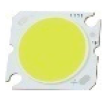
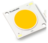
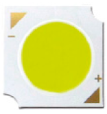
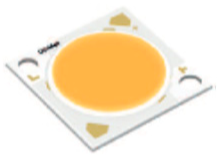
Another development was the introduction of COB LEDs at the end of the 20th century. Thanks to this, it was possible to place a few micro-LEDs (as many as a few dozen on 1 cm2 COB surface) on a small surface (up to a few cm2). Thanks to such a solution and ongoing improvements of micro-chip luminous efficiency, COB LEDs obtain a luminous flux exceeding 20,000 lm. This significantly contributed to the development of new possible applications of LEDs. However, as the number and density of high-efficiency micro-chips grows in COB LEDs, the power of such light sources increases. Currently, with maximum program parameters, COB LEDs with powers exceeding as much as 300 W can be found on the market. This causes construction problems connected with the need to dissipate heat from a small surface, which is a serious issue for thermal system producers and constructors [30,31]. Moreover, the size of COB LED results in the need to use special, dedicated optical system constructions [32,33]. According to the latest research, limiting the Tj junction temperature is of key importance to the life of light-emitting diodes [34]. Exceeding the maximum Tj junction temperature set by producers can irreversibly damage a LED [35,36].
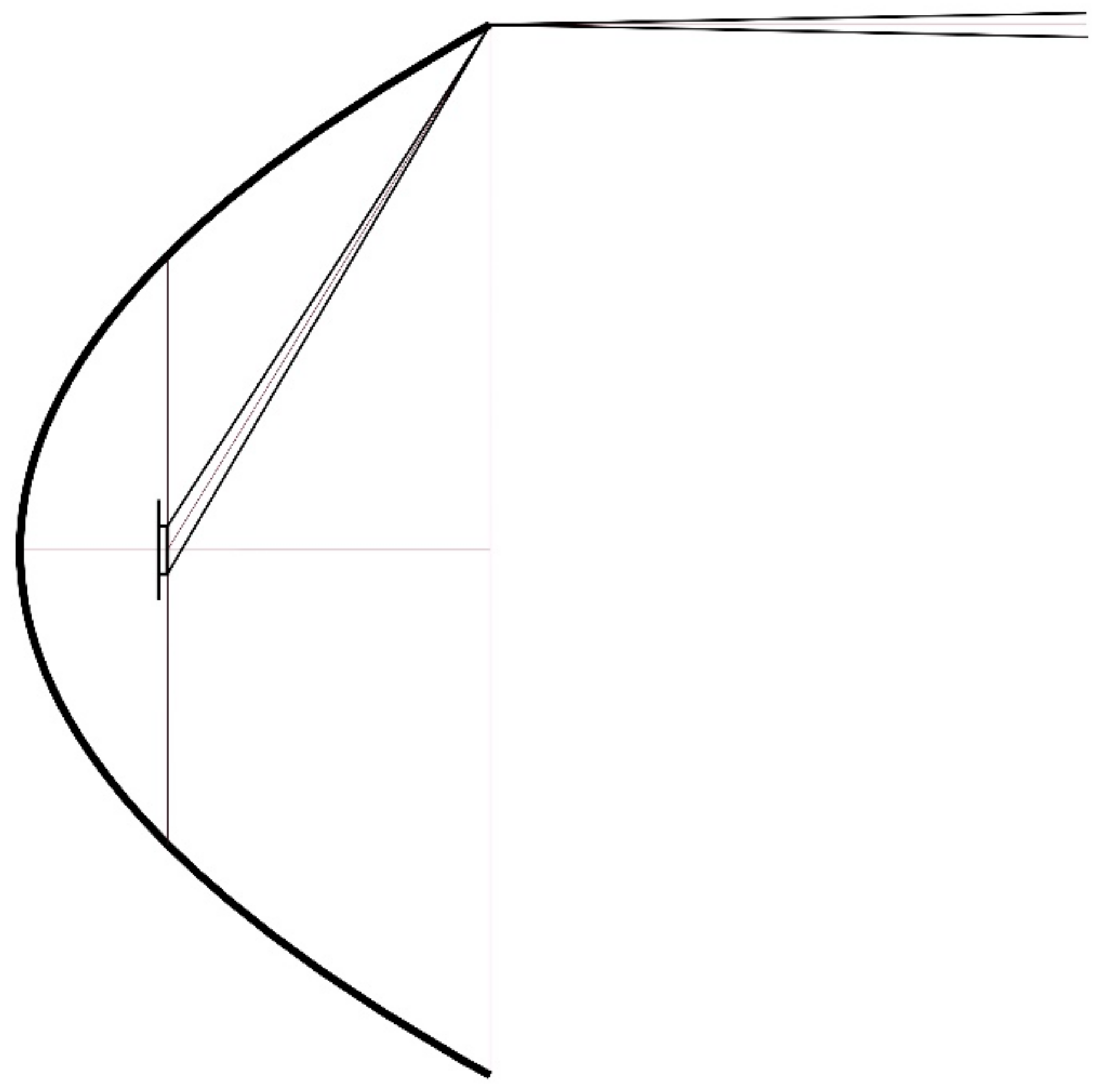
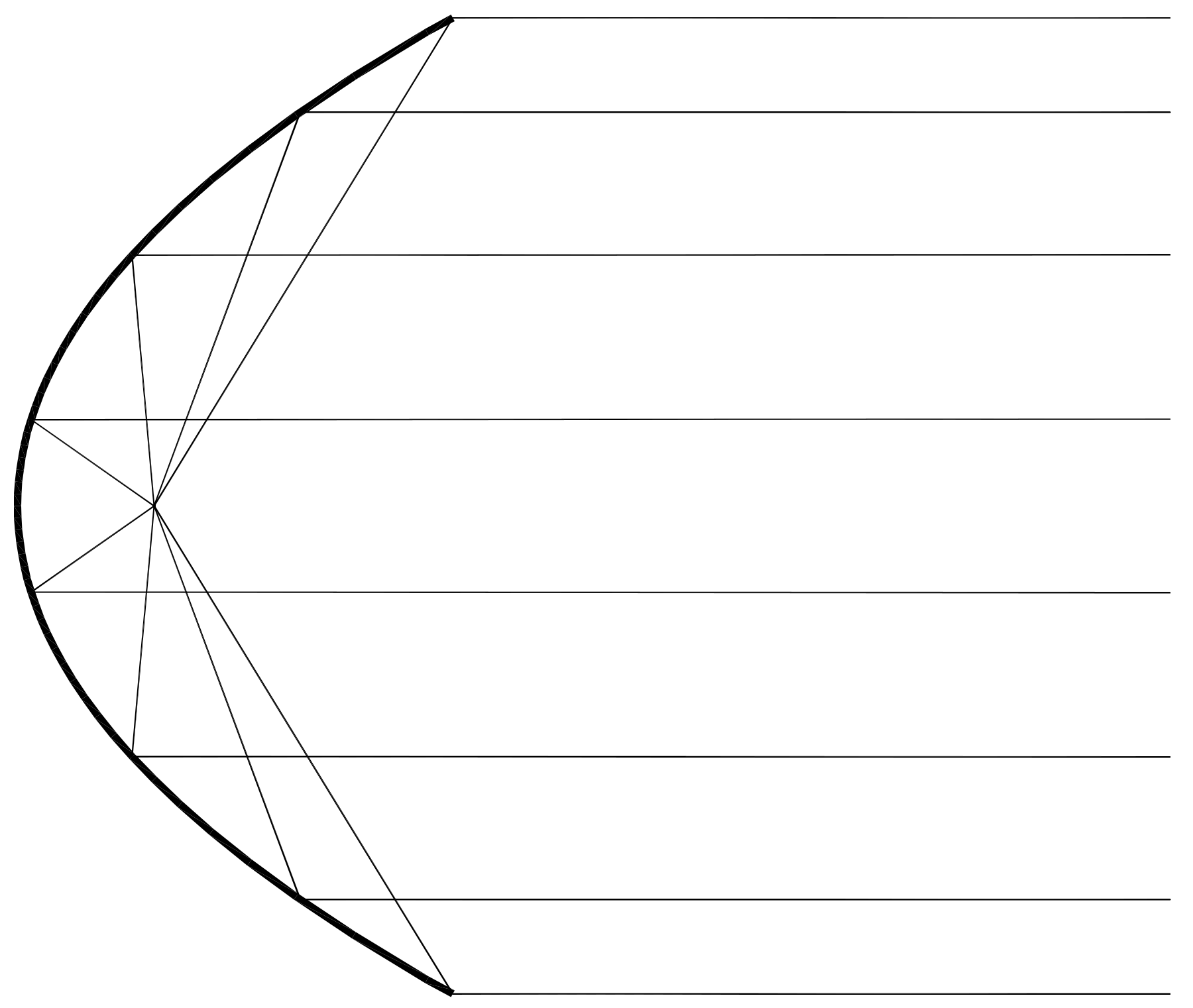
For each optical system designer, knowing the luminance level and luminance distribution (including its gradient) on the light source surface is critical regardless of the type of light source used. In order to obtain high optical system amplification, it is best when the shape of the light source is similar to the light point and has high luminance. For paraboloidal systems, luminous flux angular density is the greatest (Figure 1) with minimal divergence of luminous flux.
When the light source is not a point one, as in the case of COB LEDs, there is a divergence of the luminous flux reflected off the optical systems (e.g. paraboloidal reflector). The bigger the light source, the greater the divergence (Figure 2). In this case, luminance distribution on the light source surface has a significant influence on the lighting manner. Other complex optical constructions influencing lighting uniformity in a positive manner have been documented in the literature [37,38].
It is worth mentioning that a small number of publications on lighting technology have been devoted to examining luminance distributions on LED surfaces [8,39,40,41,42,43] or LED luminance models [44,45], and even fewer have been devoted to research on COB LED luminance [46].
The main objectives of the research were to establish luminance distribution on the surface of selected COB LEDs, to establish the luminance gradient, and to observe the dependence of luminance distribution on changing the observation direction. The additional goal was to determine the place where the maximum luminance occurs on the surface of examined light-emitting diodes.

2. Materials and Methods

2.1. Selection and Description of COB LEDs Used in the Research

Six COB LEDs of various producers, whose names will not be provided, were selected to present the research results from among many examined light sources. The main criteria of the light sources’ selection were their popularity and wide availability. The chosen light-emitting diodes varied in terms of their photometric and electric parameters (luminous flux, rated current, rated voltage, power). The solid of the luminous intensity distribution of all COB LEDs selected for the tests was similar to Lambert’s distribution. During COB LED selection for the research, a special attention was paid to photometric parameters remaining stable during the measurements.
The most important technical parameters of COB LEDs selected for research are presented in Table 1 and ordered in terms of luminous surface size.
Table 2 presents the values of total heat transfer resistance. For the surrounding temperature of 20 °C and LED-rated load, the expected mean connector temperatures were also determined. Moreover, Table 2 specifies luminous efficacy for the examined COB LEDs.

2.2. The Description of the Measurement Stand

The tests were conducted in a photometric darkroom of the photometry and colorimetry laboratory of the Lighting Technology Division at Warsaw University of Technology. A measurement stand, presented in Figure 3, was put together for the tests. A specially designed goniophotometer (1) was the main element of the setup. This goniophotometer made mounting of both a radiator (a specially designed cooling system (2)) and the examined COB LEDs (3) possible. The mentioned above system allowed the light-emitting diodes to be examined in a (C, γ) system. Prior to measurements, the light-emitting diodes were positioned using two lasers (4) and two micrometric screws (5) located on the measurement table (6). The thermal conditions of LEDs were controlled using Tes 1311A temperature meter (TES Electrical Electronic Corp., Taipei, Taiwan) (7) with 0.1 K resolution. The meter was coupled with a K-type blanket thermocouple TP 201 (Czaki Thermo-Product, Raszyn-Rybie, Poland). The diodes were powered with Stabilized DC power supply (Unitra, Warsaw, Poland) (10). Direct luminance measurements were conducted using luminance and color measuring camera LMK98-3 Color (TechnoTeam Bildverarbeitung GmbH, Ilmenau, Germany) (8), which was mounted on the goniophotometer. The correct measurement lens (TechnoTeam Bildverarbeitung GmbH, Ilmenau, Germany) (9) was selected for the luminance measuring device, and then a correct measurement distance was determined for the COB LED image to be projected on the biggest possible CCD matrix surface. The luminance measuring device lens was equipped with gray filters that allowed COS LED luminance to be decreased to a level that could be registered directly by the luminance measuring device. The electric parameters were controlled using laboratory multimeters (11). The goniometer was operated using dedicated software (Spektrokolor, Lodz, Poland) installed on a laptop (12), and the results from the LMK camera were also registered using dedicated software installed on the laptop (12).
The measurements were made in predefined conditions. The temperature of the examined COB LEDs was similar thanks to the application of large-sized heat sinks. It was assumed in the tests that the relatively small differences between the expected connectors’ temperatures should not cause significant differences in the catalogue data regarding radiation emission and temperature distribution.

3. Results

The first stage of the research was to determine and analyze luminance distribution from the optic axis direction. Moreover, changes in mean and maximum luminance were established for different areas marked on the examined COB LEDs. The areas marked for analysis were compliant with the COB LED shape and occupied respectively: 0.5%, 1%, 5%, 10%, 25%, 50%, 75% and 100% of the COB LED luminous surface, as shown in Figure 4. The center of the marked areas was in the COB LED geometric center. Thanks to this analysis, it was possible to determine which area the maximum COB LED luminance was in. At the same time, it was determined whether this area was the smallest (among the analyzed ones) and closest to the diode’s geometric center, which is the most significant in terms of designing optical systems.
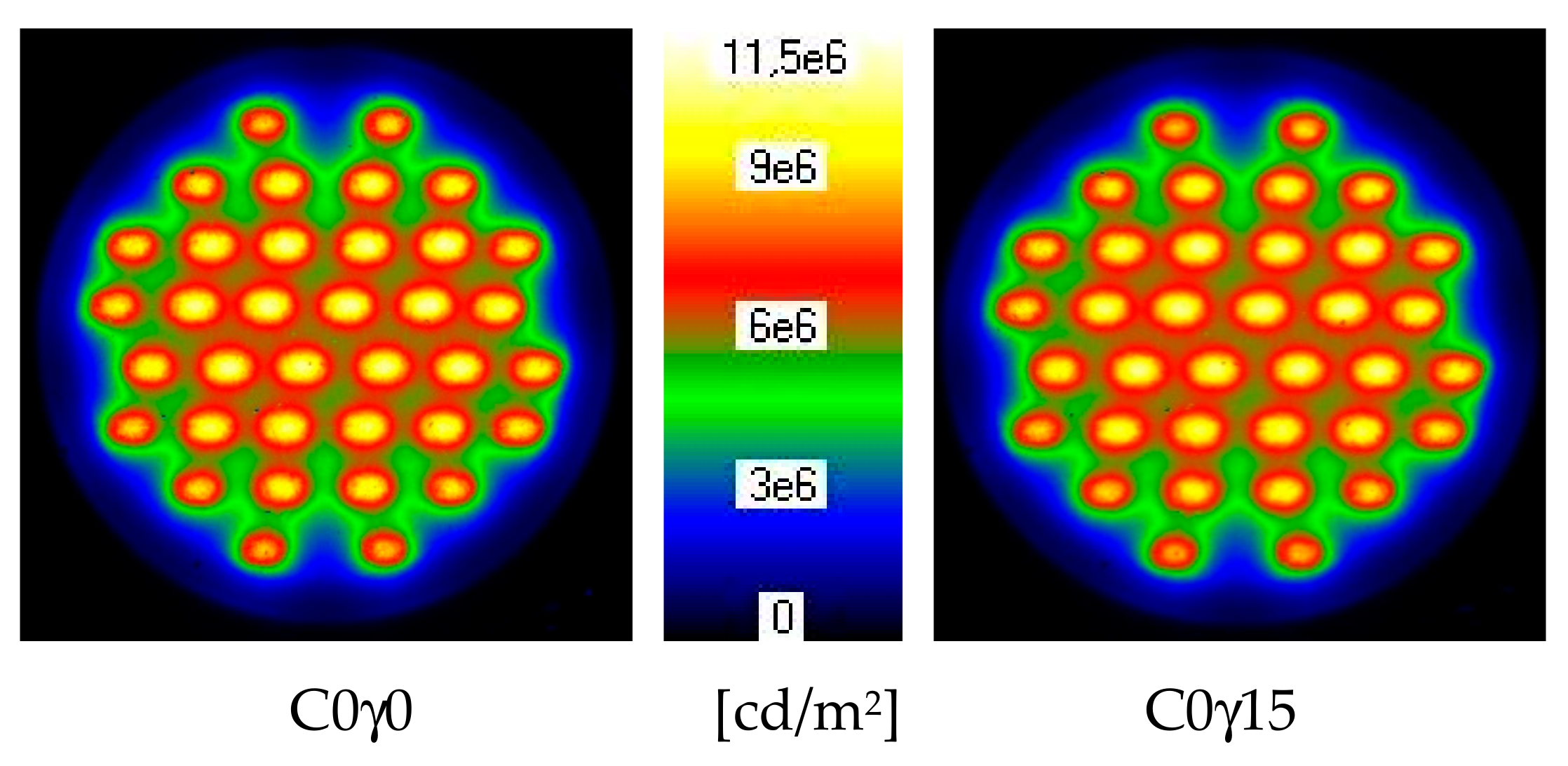
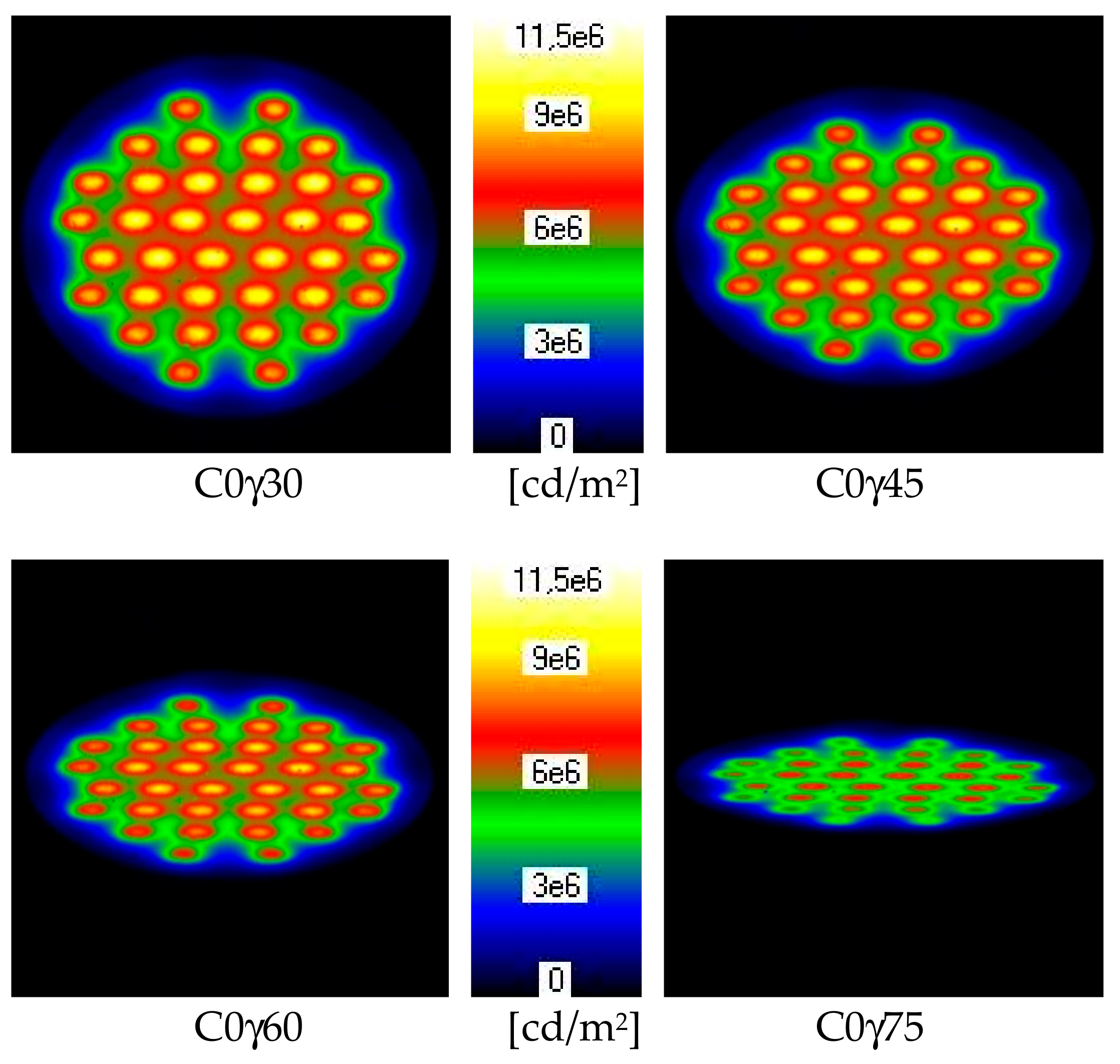
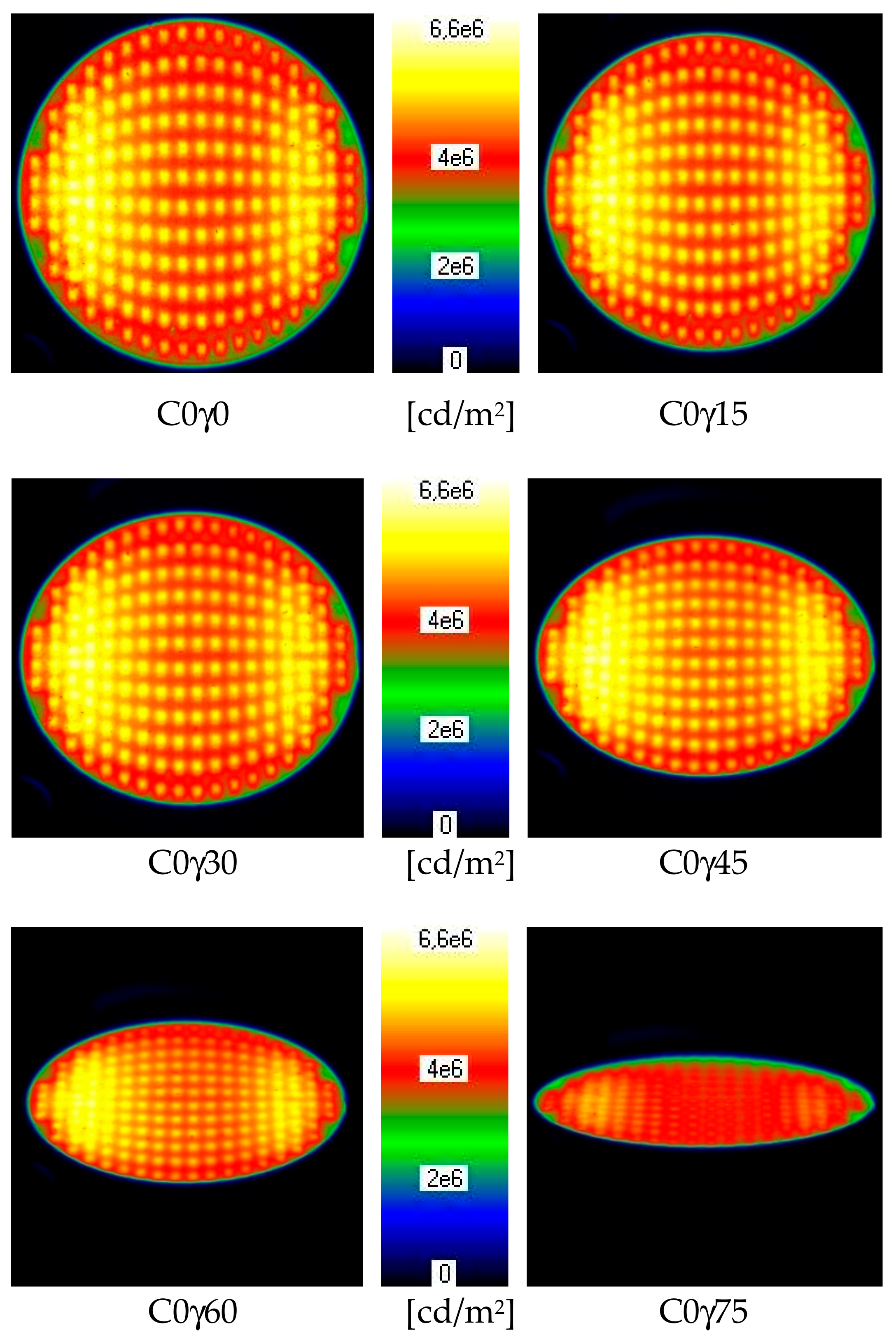
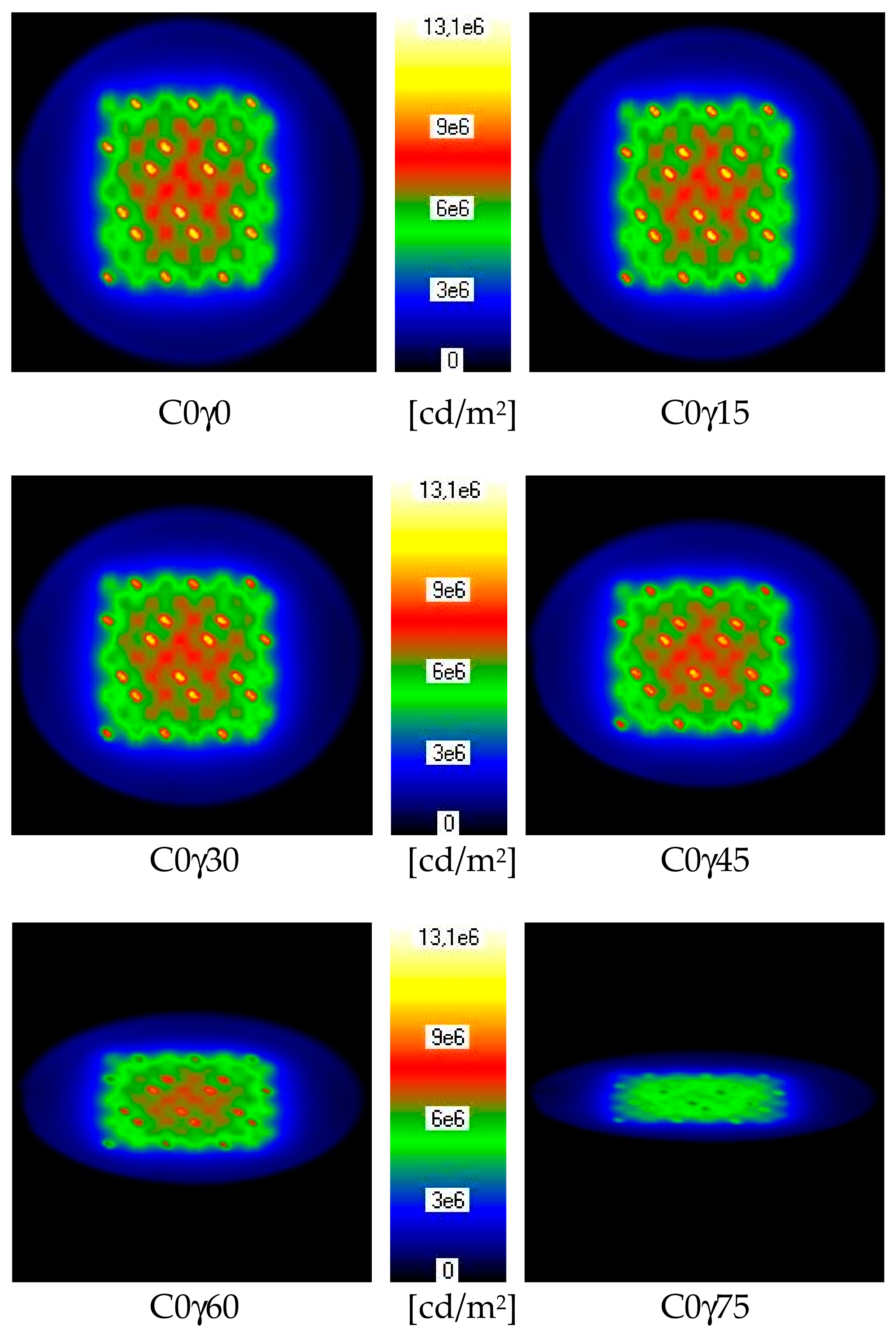
The next stage of the research was to examine luminance distributions on the COB LED surface for different observation directions in the (C,γ) system. C semi-planes were changed every 15° and γ angles every 5°.The results for C0 semi-plane and γ angles changed every 15° and were selected in order to present the research results clearly. The presentation of results for C0γ90 was abandoned, as for each angle, the light-emitting diodes did not shine (black image). For this reason, subsequent images present luminance distributions of specific COB LEDs (COB1, COB3 and COB6 were selected for presentation) for six observation directions: C0γ0, C0γ15, C030, C0γ45, C0γ60, and C0γ75.
Figure 5 presents luminance distributions on COB1 surface (350mA current) for different observation directions.
Figure 6 presents luminance distributions on the COB4 surface (720 mA current) for different observation directions.
Figure 7 presents luminance distributions on the COB6 surface (1280 mA current) for different observation directions.

4. Discussion

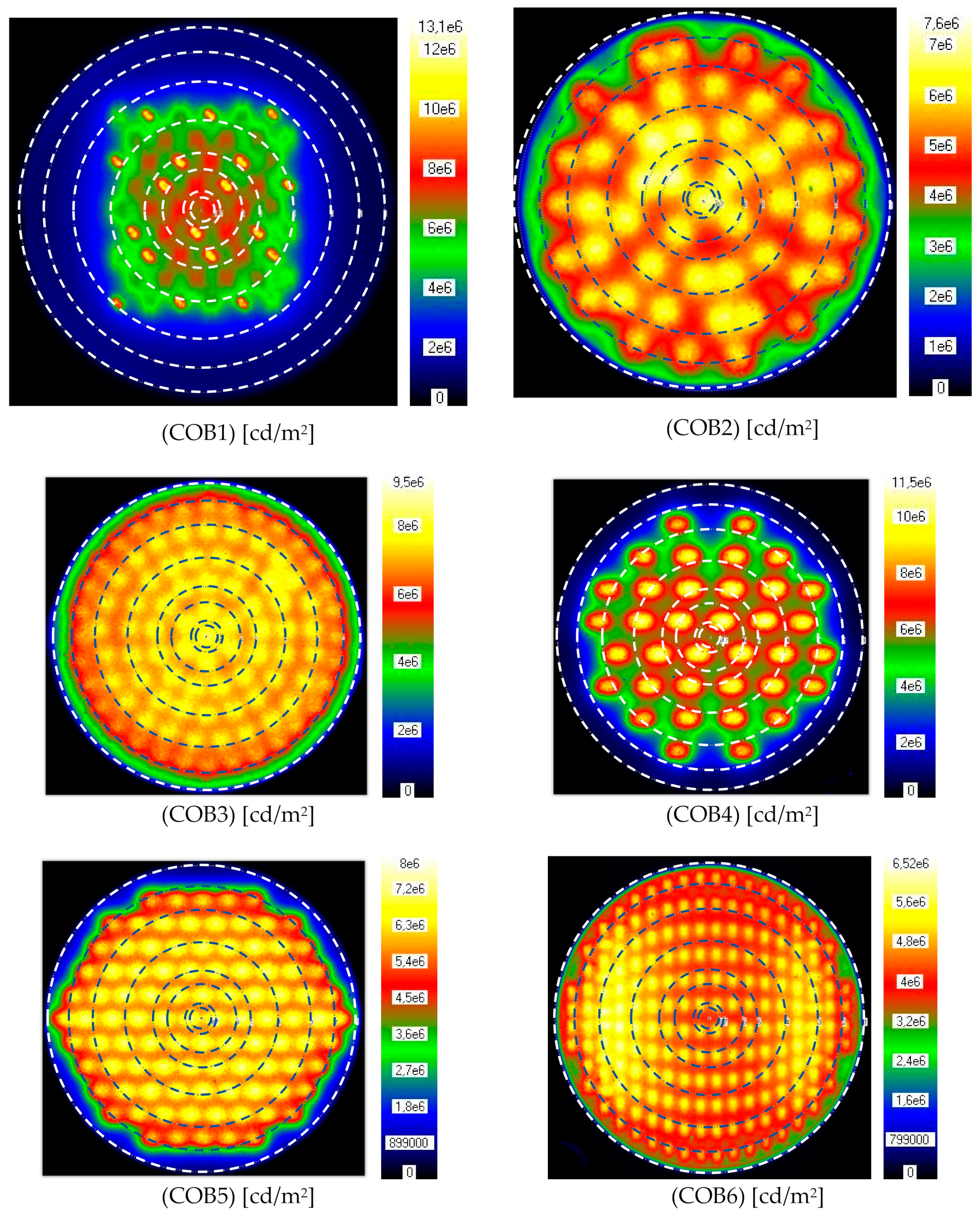
The first analyzed parameter was the way in which the micro-chip LED (micro-LED) was located on the COB LED surface. It was noted that on all examined COB LEDs, the arrangement of micro-LEDs was different. So, no standard in this respect was clearly visible. Moreover, it was observed that micro-LEDs were evenly placed in the cases of COB3, COB5 and COB6, while a certain irregularity was noted in the case of COB1 (Figure 4). It was also noted that the manner in which micro-LEDs are arranged determines the luminance distribution on the COB LED surface. All the presented COB LEDs were circular in shape. However, the arrangement of micro-LEDs resulted in the dominant luminance, for example, COB5 were contained in the shape of a regular hexagon or in the case of COB1, in a square shape (Figure 4). It was also noticed that the micro-LEDs create local luminance. This influences temperature distribution on COB LED surfaces. For example, in the case of COB3, the maximum luminance of one of the micro-LEDs in the COB center was 9.39 × 10⁶ cd/m2, and in the area on the COB edge on one of the micro-LEDs it dropped to 8.05 × 10⁶ cd/m2. The situation was similar with the remaining COB LEDs, with the exception of COB1 and COB6. In COB1, the micro-LEDs were arranged in the shape of a rectangle, and the maximum luminance in local maximums on the edge of the shape fluctuated from 5.25 × 10⁶ cd/m2 to 12.68 × 10⁶ cd/m2, i.e. closest to the highest luminance on the COB LED surface (13.06 × 10⁶ cd/m2).
The next stage of the research was to establish and analyze luminance distribution from the optical axis direction. For this purpose, the areas of analysis were marked on the examined COB LEDs, which corresponded to the shape of COB LEDs and occupied respectively: 0.5%, 1%, 5%, 10%, 25%, 50%, 75% and 100% of the COB LED luminous surface, as shown in Figure 4. The results of the research for each area where the mean luminance, maximum luminance and minimum luminance were determined, are presented in Table 3 and Table 4.
On the basis of the conducted research, it can be concluded that the maximum luminance is not always located in the COB LED center or even in the area closest to the center (area no. 8). Only in the case of COB2 and COB3, the maximum luminance is located in the defined smallest area in the center of COB. In the remaining cases, the maximum luminance occurs outside the area closest to the center of the examined COB.
Moreover, it was concluded that the greater the test area, the smaller the mean luminance (for all COB LEDs (except COB6) for surfaces over 50%, areas no. 3, no. 2 and no. 1). This results from the previously mentioned method of micro-LED distribution and conditions of temperature distribution on COB LED surfaces. Due to the location of the local maximum luminance in the cases of COB4 and COB6, as the test area grows (from area no. 8 to area no. 1), the mean luminance at the beginning increases and then it decreases respectively for surfaces over 5% and 50% (respectively for COB4 and COB6).
The greatest disproportion between the maximum and mean luminance, measured for the entire COB LED surface (area no. 1), occurred for COB1, but it was also high for COB4. The maximum luminance was on COB1, which was over four times higher than the mean luminance (hence the greatest luminance gradient on COB1). The smallest luminance gradient was on COB3 and COB6 where the maximum luminance was 39% and 47% higher than the mean luminance (the smallest luminance gradient among the examined COB), as shown in Figure 4.
The next stage of the analysis was determining the influence of changes of COB LED observation angle and luminance distribution on its surface. Analyzing the luminance distribution, it was concluded that mean luminance level varies along with the observation angle, which does not adhere to Lambert’s law. Light distribution in accordance with Lambert’s law is often discussed in the literature [47,48]. Generally, the spatial distribution of light is in accordance with Lambert’s law if the light changes according to the cosine function, and the luminance is constant for each direction of observation (distribution). This was not the case here.
As the observation angle changes (in (C, γ) system gamma angles from 0° to 90°), the mean luminance, minimum luminance and maximum luminance all decrease. The influence of observation angle on mean luminance is depicted in Table 5, while the influence of the observation angle on maximum and minimum luminance is presented respectively in Table 6 and Table 7.
Analyzing the results of the conducted research, it was concluded that as the observation angle (γ) changes, the mean, maximum and minimum luminances also change. The mean luminance, for observation angle γ = 60° was on the level of over 90% of mean luminance obtained for angle γ = 0° (axial), where angle γ = 0° was treated as the point of reference. For angle γ = 75°, it was still on the level of 70% of the reference (axial) luminance. Moreover, it was observed that as the observation angle (γ) increases, the mean luminance usually decreases. However, for three COB LEDs, an increase in luminance was noted, i.e. the greatest value of mean luminance for COB 1 was for γ = 30° and γ = 45°, COB2 for γ = 15°, and COB6 for γ = 45°.
In the case of maximum luminance, the tendency of luminance to change as the observation angle increases is essentially similar to the mean luminance. For five COB LEDs, for angle γ = 45°, the maximum luminance was over 92% of the maximum luminance measured on the COB LED axis (for γ = 0°), except for COB1 where the maximum luminance was over 83% of the axial luminance. Practically, in all cases (except COB6), the maximum luminance decreased as the observation angle increased. For angle γ = 75°, the maximum luminance dropped to the level of approximately 70% of maximum luminance measured in the axis (except for COB1 where it dropped to 54%; the reason for this could have been a different construction and location of micro-LEDs). In the case of minimum luminance, a considerable influence of the measurement field marking precision on measurement results was noticed. However, the changes tendency, i.e. luminance dropped as the observation angle increased, was similar to mean and maximum luminance.
Moreover, as the observation angle increased, no considerable deformations of COB luminous surfaces were noticed. In earlier research, it was observed that deformation of the luminous surface occurs in the case of the LED with an additional (secondary) optical system, in particular in the case of Side Emitting (SE) LEDs.
As anticipated and following the theory, the size of the luminous surface changed in accordance with the cosinus function.

5. Conclusions

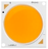
The increasingly bigger power of the produced COB LEDs, and as a result their bigger luminous flux, makes it possible for these light sources to be put to various uses. In practice, however, when buying COB LED, we only see a yellow surface, usually in the shape of a circle or a rectangle. Interestingly, circular COB was selected for the tests and only during the research it appeared that the micro-chips were not always arranged in a circle, but also in a hexagon (COB5) or a square (COB1). Moreover, no information about luminance distribution was found in light source catalogue data. It is the familiarity with the luminance distribution on COB LED surfaces that is a vital and essential piece of information in designing optical systems for such a light source.
In order to determine luminance distribution on COB surfaces, six COB LED pieces of a few well-known producers were chosen for the tests. Diodes of different sizes and micro-chip arrangements were selected for the tests. A great diversity in micro-chip arrangement and no standards in this respect were observed during the tests. A certain irregularity in micro-chip arrangement in one of the examined COB LEDs was noticed (COB1).
The following, among others, influence uniform luminance distribution on COB surfaces: the number of applied micro-LEDs, layout of micro-LEDs, micro-LEDs’ size, type and thickness of the used luminophore, and uniform distribution of the semiconductor’s structure temperature. Moreover, but to a lesser extent, in the case of COB LED, light emissions from micro LED’s side wall can also have some influence (however, luminophore partially limits this influence). On the basis of the conducted tests, it was concluded that one of the most uniform luminance distributions (the lowest gradient of change) occurred on COB6. The following factors contributed to this: A large number of used micro-LEDs and their uniform layout. The producer correctly selected the luminophore composition and provided uniform heat distribution in the semiconductor structures. It was noted that maximum luminance areas occurred in high micro-LED density areas or in places where heat transfer to the heat sink was the best and the local temperatures were the lowest (as in the case of COB6).
The conducted tests showed that all of the examined light sources have uneven luminance distribution. The greatest luminance gradient was on COB1 due to the rectangular arrangement of micro-chips on the circular surface. It was also observed that micro-LEDs create local luminance maximus. It was concluded that the greatest luminance occurs where the micro-chip density is the greatest and that the greatest luminance does not always occur in the COB LED center.
This is particularly important when designing optical systems as a designer needs to know where the maximum luminance occurs and take advantage of this fact.
If amplifying the system is crucial for the optical system designer, it will be desirable for the maximum luminance to be focused in the area of the light source center. If uniform lighting from the optical system is the designer’s priority, then COB LED should have the most uniform luminance distribution possible.
It was shown that as the COB LED observation angle changes, their mean and maximum luminance changes. The mean luminance for observation angle γ = 60° was on the level of over 90% of mean luminance for the axial angle. For even greater angles (up to γ = 75°), it remained on a high level (over 70% of axial luminance). It can therefore be concluded that COB LED, also for considerable observation angles, still remains a light source that can cause a discomfort glare. It was additionally concluded that there was no compliance of light emission from the COB LED surface with Lambert’s law.
The obtained results have led to the conclusion that designing optical systems for COB LED needs to consider irregular luminance distribution on their surface. The next stage of the research will be to determine the influence of unevenness of COB LED luminance distribution on the light distribution solid of the designed lighting fitting.

Funding

The author would like to express his gratitude to the Signify Poland for funding and the possibility of publishing the results of the conducted research.

Acknowledgments

The author would like to express his gratitude to the Signify Poland for funding the possibility of publishing the obtained results research.

Conflicts of Interest

The author declare no conflict of interest.

References

  1. Cree. Cree First to Break 300 Lumens-Per-Watt Barrier. Available online: http://www.cree.com/news-media/news/article/cree-first-to-break-300-lumens-per-watt-barrier (accessed on 3 July 2017).
  2. Bommel, W. Road Lighting. Fundamentals, Technology and Application; Springer International Publishing: Berlin/Heidelberg, Germany, 2015; pp. 1–334. [Google Scholar]
  3. Chunyun, X.; Haobo, C.; Yunpeng, F. Optical design of rectangular illumination with freeform lenses for the application of LED road lighting. Front. Optoelectron. 2017, 10, 353–362. [Google Scholar]
  4. Zalewski, S. Design of optical systems for LED road luminaires. Appl. Opt. 2015, 54, 163–170. [Google Scholar] [CrossRef] [Green Version]
  5. Hu, X.; Qian, K. Optimal design of optical system for LED road lighting with high illuminance and luminance uniformity. Appl. Opt. 2013, 52, 5888–5893. [Google Scholar] [CrossRef]
  6. Czyżewski, D. The street lighting luminaires with LEDs. Przegląd Elektrotechniczny 2009, 86, 276–279. [Google Scholar]
  7. Christensen, A.; Graham, S. Thermal Effects in Packaging High Power Light Emitting Diode Arrays. Appl. Therm. Eng. 2009, 29, 364–371. [Google Scholar] [CrossRef]
  8. Tyukhova, Y.; Waters, C.E. An assessment of high dynamic range luminance measurements with LED lighting. Leukos 2014, 10, 87–99. [Google Scholar] [CrossRef] [Green Version]
  9. Tashiro, T.; Kawanobe, S.; Kimura-Minoda, T.; Kohko, S.; Ishikawa, T.; Ayama, M. Discomfort glare for white LED light sources with different spatial arrangement. Lighting Res. Technol. 2015, 47, 316–337. [Google Scholar] [CrossRef]
  10. Yang, Y.; Ma, S.N.; Luo, M.R.; Liu, X.Y. Discomfort glare Caused by Non-uniform white LED Matrices. In Proceedings of the 28th CIE Session, Manchester, UK, 28 June–4 July 2015; pp. 393–399. [Google Scholar]
  11. Tashiro, T.; Kawanobe, S.; Kimura-Minoda, T.; Kohko, S.; Ishikawa, T.; Ayama, M. Discomfort glare for white LED light sources with different spatial arrangements. Light. Res. Technol. 2015, 47, 316–337. [Google Scholar] [CrossRef]
  12. Geerdinck, L.M.; Van Gheluwe, J.R.; Vissenberg, M.C.J.M. Discomfort glare perception of non-uniform light sources in an office setting. J. Environ. Psychol. 2014, 39, 5. [Google Scholar] [CrossRef]
  13. Pakkert, M.; Rosemann, A.L.P.; van Duijnhoven, J.; Donners, M. Glare quantification for indoor volleyball. Build. Environ. 2018, 143, 48–58. [Google Scholar] [CrossRef]
  14. Davis, W.; Ohno, Y. Approaches to color rendering measurement. J. Mod. Opt. 2009, 56, 1412–1419. [Google Scholar] [CrossRef]
  15. Method of Measuring and Specifying Colour Rendering Properties of Light Sources; Technical Report CIE 013.3–1995; CIE: Vienna, Austria, 1995.
  16. Houser, K.; Mossman, M.; Smet, K.; Whitehead, L. Tutorial: Color Rendering and Its Applications in Lighting. Leukos 2016, 12, 7–26. [Google Scholar] [CrossRef] [Green Version]
  17. Zukauskas, A.; Shur, M.S. Color Rendering Metrics: Status, Methods and Future Development. Handb. Adv. Light. Technol. 2017, 799–827. [Google Scholar]
  18. Colour Fidelity Index for Accurate Scientific Use; Technical Report CIE 224:2017; CIE: Vienna, Austria, 2017.
  19. Chen, Y.S.; Lin, C.Y.; Yeh, C.M.; Kuo, C.T.; Hsu, C.W.; Wang, H.C. Anti-glare LED lamps with adjustable illumination light field. Opt. Express 2014, 22, 5183–5195. [Google Scholar] [CrossRef] [PubMed]
  20. Rózanowska, M.; Jarvis-Evans, J.; Korytowski, W.; Boulton, M.E.; Burke, J.M.; Sarna, T. Blue light-induced reactivity of retinal age pigment in vitro generation of oxygen-reactive species. J. Biol. Chem. 1995, 35, 18825–18830. [Google Scholar] [CrossRef] [PubMed] [Green Version]
  21. Jakubowski, P.; Fryc, I. Metrological requirements for measurements of circadian radiation. Opt. Appl. 2018, 48, 697–704. [Google Scholar]
  22. Rea, M.S.; Figueiro, M.; Bullough, J.D. Circadian photobiology: An emerging framework for lighting practice and research. Light. Res. Technol. 2002, 34, 177–187. [Google Scholar] [CrossRef]
  23. Brainard, G.C.; Hanifin, J.P.; Greeson, J.M.; Byrne, B.; Glickman, G.; Gerner, E.; Rollag, M.D. Action Spectrum for Melatonin Regulation in Humans: Evidence for a Novel Circadian Photoreceptor. J. Neurosci. 2001, 21, 6405–6412. [Google Scholar] [CrossRef] [Green Version]
  24. Fryc, I.; Tabaka, P. Outdoor Areas Lighting with LEDs-the Competition Between Scotopic Efficacy and Light Pollution. Photon. Lett. Pol. 2019, 11, 75–77. [Google Scholar] [CrossRef]
  25. Brons, J.A.; Bullough, J.D.; Rea, M.S. Outdoor site-lighting performance: A comprehensive and quantitative framework for assessing light pollution. Light. Res. Technol. 2008, 40, 201–224. [Google Scholar] [CrossRef]
  26. Gou, F.; Hsiang, E.L.; Tan, G.; Chou, P.T.; Li, Y.L.; Lan, Y.F.; Wu, S.T. Angular color shift of micro-LED displays. Opt. Express. 2019, 27, 746. [Google Scholar] [CrossRef] [PubMed]
  27. Bai, S.; Yuan, Z.; Gao, F. Colloidal metal halide perovskite nanocrystals: Synthesis, characterization, and applications. J. Mater. Chem. C 2016, 4, 3898–3904. [Google Scholar] [CrossRef] [Green Version]
  28. He, Z.; Zhang, C.; Dong, Y.; Wu, S.T. Emerging Perovskite Nanocrystals-Enhanced Solid-State Lighting and Liquid-Crystal Displays. Crystals 2019, 9, 59. [Google Scholar] [CrossRef] [Green Version]
  29. He, Z.; Zhang, C.; Chen, H.; Dong, Y.; Wu, S.-T. Perovskite Downconverters for Efficient, Excellent Color-Rendering, and Circadian Solid-State Lighting. Nanomaterials 2019, 9, 176. [Google Scholar] [CrossRef] [PubMed] [Green Version]
  30. Seher, A.; Yurtseven, M.B.; Onaygil, S. Design of a chip on board (cob) led based industrial luminaire with thermal simulations. Light Eng. 2019, 27, 78–87. [Google Scholar]
  31. Ha, M.; Graham, S. Development of a thermal resistance model for chip-on-board packaging of high power LED arrays. Microelectron. Reliab. 2012, 52, 836–844. [Google Scholar] [CrossRef]
  32. Ge, A.; Shu, H.; Chen, D.; Cai, J.L.; Chen, J.Y.; Zhu, L. Optical design of a road lighting luminaire using a chip-on-board LED array. Light. Res. Technol. 2017, 49, 651–657. [Google Scholar] [CrossRef]
  33. Hao, R.; Ge, A.; Tao, X.; Liu, Y.; Zhao, B.; Yang, E. Optical design of a high-mast luminaire based on four COB LED light source modules. Light. Res. Technol. 2019, 51, 447–456. [Google Scholar] [CrossRef]
  34. Baran, K.; Różowicz, A.; Wachta, H.; Różowicz, S.; Mazur, D. Thermal Analysis of the Factors Influencing Junction Temperature of LED Panel Sources. Energies 2019, 12, 3941. [Google Scholar] [CrossRef] [Green Version]
  35. Poppe, A.; Farkas, G.; Gaal, L.; Hantos, G.; Hegedus, J.; Rencz, M. Multi-Domain Modelling of LEDs for Supporting Virtual Prototyping of Luminaires. Energies 2019, 12, 1909. [Google Scholar] [CrossRef] [Green Version]
  36. Ahn, B.; Park, J.; Yoo, S.; Kim, J.; Jeong, H.; Leigh, S.; Jang, C. Synergetic Effect between Lighting Efficiency Enhancement and Building Energy Reduction Using Alternative Thermal Operating System of Indoor LED Lighting. Energies 2015, 8, 8736–8748. [Google Scholar] [CrossRef] [Green Version]
  37. Zhu, R.; Hong, Q.; Zhang, H.; Wu, S.T. Freeform reflectors for architectural lighting. Opt. Express 2015, 23, 31828–31837. [Google Scholar] [CrossRef] [PubMed]
  38. Sun, C.C.; Lee, X.H.; Moreno, I.; Lee, C.H.; Yu, Y.W.; Yang, T.H.; Chung, T.Y. Design of LED Street Lighting Adapted for Free-Form Roads. IEEE Photon. J. 2017, 9, 1–13. [Google Scholar] [CrossRef]
  39. Jongewaard, M. Guide to selecting the appropriate type of light source model. In Proceedings of the SPIE 47th Annual Meeting 2002, Seattle, WA, USA, 7–11 July 2002. [Google Scholar]
  40. Czyżewski, D. Luminance distribution of LED luminous sufface. Przegląd Elektrotechniczny 2010, 86, 166–169. [Google Scholar]
  41. Słomiński, S. Selected Problems in Modern Methods of Luminance Measurement of Multisource LED Luminaires. Light Eng. 2016, 24, 45–50. [Google Scholar]
  42. Zheng, L.; Guo, Z.; Yan, W.; Lin, Y.; Lu, Y.; Kuo, H.C.; Chen, Z.; Zhu, L.; Wu, T.; Gao, Y. Research on a Camera-Based Microscopic Imaging System to Inspect the Surface Luminance of the Micro-LED Array. IEEE Access 2018, 6, 51329–51336. [Google Scholar] [CrossRef]
  43. Czyżewski, D. Selected problems of defining the luminous area of electroluminescent diodes. Przegląd Elektrotechniczny 2008, 84, 125–128. [Google Scholar]
  44. Jongewaard, M.; Wilcox, K. LED source models. LED J. 2009, 64–72. [Google Scholar]
  45. Słomiński, S. Luminance mapping to the light source model-possibilities to use a MML in the lighting technology field. Przeglad Elektrotechniczny 2011, 4, 87–89. [Google Scholar]
  46. Czyżewski, D. Investigation of COB LED luminance distribution. In Proceedings of the 2016 IEEE Lighting Conference of the Visegrad Countries (Lumen V4), Karpacz, Poland, 13–16 September 2016. [Google Scholar]
  47. Gall, D. Grundlagen der Lichttechnik: Kompendium, 2nd ed.; Richard Pflaum Verlag GmbH & Co. KG: München, Germany, 2007; pp. 1–217. [Google Scholar]
  48. Schubert, E.F. Light-Emitting Diodes, 3rd ed.; Cambridge University Press: Cambridge, UK, 2018; pp. 1–672. [Google Scholar]
Figure 1. Theoretic light system: point light sources and paraboloidal mirror reflector.
Crystals 09 00645 g001
Figure 2. Luminous flux divergence in non-point light source (mirror paraboloidal system).
Crystals 09 00645 g002
Figure 3. Measurement stand diagram.
Crystals 09 00645 g003
Figure 4. COB1, COB2, COB3, COB4, COB5, and COB6 with six plotted measurement areas on luminance distributions from the optic axis direction (C0γ0).
Crystals 09 00645 g004
Figure 5. COB1—luminance distribution for different observation directions (C0γ0 ÷ 75).
Crystals 09 00645 g005
Figure 6. COB4—luminance distribution for different observation directions (C0γ0 ÷ 75).
Crystals 09 00645 g006aCrystals 09 00645 g006b
Figure 7. COB6—luminance distribution for different observation directions (C0γ0 ÷ 75).
Crystals 09 00645 g007
Table 1. Technical parameters selected for COB LED presentation.
Basic Technical ParametersCOB1COB2COB3COB4COB5COB6
COB LED View 1 Crystals 09 00645 i001 Crystals 09 00645 i002 Crystals 09 00645 i003 Crystals 09 00645 i004 Crystals 09 00645 i005 Crystals 09 00645 i006
Maximum dimension9.3 mm13 mm15 mm17 mm17.5 mm22 mm
Typical luminous flux (85 °C)810 lm1825 lm3650 lm2325 lm4080 lm5905 lm
Color rendering index (CRI)858080809080
Correlated color temperatures (CCT)3200 K3000 K3000 K3200 K3000 K5000 K
Typical forward Current0.350 A0.450 A0.900 A0.720 A1.040 A1.280 A
Wattage9W16 W32 W24W48 W45W
Maximum junction temperature150 °C125 °C125 °C150 °C125 °C140 °C
Thermal resistance0.6 °C/W0.55 °C/W0.29 °C/W1.4 °C/W0.5 °C/W0.37 °C/W
1 COB LED photos were taken from catalogues of the light-source producers.
Table 2. Designated technical parameters for specific COB LEDs.
Designated Technical ParametersCOB1COB2COB3COB4COB5COB6
Thermal resistance, (°C/W)2.001.951.692.201.301.17
Junction temperature (°C)38.051.274.172.882.472.65
light efficiency (lm/W)901141149785131
Table 3. Mean luminance, maximum luminance and minimum luminance for different areas of examined COB LED surfaces (COB1, COB2, COB3).
Analyzed Area on COB LED SurfaceLuminance (Mcd/m2) on COB LED Surface for Each (C0g0) Direction
COB1COB2COB3
LavrLmaxLminLavrLmaxLminLavrLmaxLmin
Area no. 87.247.906.626.507.535.758.599.398.00
Area no. 77.157.906.446.287.535.428.409.397.90
Area no. 67.1213.065.355.927.534.448.219.397.13
Area no. 57.0013.065.355.757.534.408.059.397.06
Area no. 46.4213.063.225.777.534.368.029.397.06
Area no. 35.0113.061.345.637.532.747.929.396.63
Area no. 23.8513.060.865.357.532.717.669.395.30
Area no. 13.1513.060.374.697.530.216.759.390.26
Table 4. Mean luminance, maximum luminance and minimum luminance for different areas of examined COB LED surfaces (COB4, COB5, COB6).
Analysed Area on COB LED SurfaceLuminance (Mcd/m2) on COB LED Surface for Each (C0g0) Direction
COB4COB5COB6
LavrLmaxLminLavrLmaxLminLavrLmaxLmin
Area no. 86.348.464.826.467.495.664.365.283.59
Area no. 76.7410.114.826.427.615.664.525.533.59
Area no. 67.2411.374.826.417.615.524.535.643.59
Area no. 57.1211.374.826.387.785.524.605.772.21
Area no. 47.0611.41.276.417.783.434.676.202.21
Area no. 36.6711.41.276.347.783.434.756.522.21
Area no. 25.8811.41.275.987.781.974.686.521.87
Area no. 14.6311.40.354.997.780.194.456.521.59
Table 5. Mean luminance on the examined COB LEDs surface for different observation angles.
For C0 Semi-Plane γ Observation AnglesMean Luminance (Mcd/m2) on COB LED Surface
COB1COB2COB3COB4COB5COB6
LavrLavrLavrLavrLavrLavr
γ90000000
γ453.174.566.514.514.754.59
γ303.174.686.654.564.894.49
γ153.134.736.734.614.944.42
γ03.154.696.754.704.994.45
Table 6. Maximum luminance on the examined COB LEDs surface for different observation angles.
For C0 Semi-Plane γ Observation AnglesMaximum Luminance (Mcd/m2) on COB LED Surface
COB1COB2COB3COB4COB5COB6
LmaxLmaxLmaxLmaxLmaxLmax
γ90000000
γ4510.897.048.9210.557.396.55
γ3012.017.249.2211.087.726.52
γ1512.477.479.2811.37.826.57
γ013.067.539.3911.47.786.52
Table 7. Minimum luminance on the examined COB LEDs surface for different observation angles.
For C0 Semi-Plane γ Observation AnglesMinimum Luminance (Mcd/m2) on COB LED Surface
COB1COB2COB3COB4COB5COB6
LminLminLminLminLminLmin
γ90000000
γ450.220.120.170.240.130.49
γ300.280.140.180.280.161.13
γ150.300.180.210.310.181.31
γ00.370.210.260.350.191.59

