Article

Control of Organic Superconducting Field-Effect Transistor by Cooling Rate

by
Genta Kawaguchi
1,* and
Hiroshi M. Yamamoto
1,2,*
1
Research Center of Integrative Molecular Systems (CIMoS), Institute for Molecular Science, Okazaki, Aichi 444-8585, Japan
2
RIKEN, Wako, Saitama 351-0198, Japan
*
Authors to whom correspondence should be addressed.
Crystals 2019, 9(11), 605; https://doi.org/10.3390/cryst9110605
Submission received: 12 October 2019 / Revised: 6 November 2019 / Accepted: 13 November 2019 / Published: 19 November 2019
(This article belongs to the Section Inorganic Crystalline Materials)

Abstract

:
A new superconducting field-effect transistor (FET) in the vicinity of bandwidth-controlled Mott transition was developed using molecular strongly correlated system κ-(BEDT-TTF)2Cu[N(CN)2]Br [BEDT-TTF = bis(ethylenedithio)tetrathiafulvalene] laminated on CaF2 substrate. This device exhibited significant cooling-rate dependence of resistance below about 80 K, associated with glass transition of terminal ethylene group of BEDT-TTF molecule, where more rapid cooling through glass transition temperature leads to the decrease in bandwidth. We demonstrated that the FET properties such as ON/OFF ratio and polarity can be controlled by utilizing cooling rate. Our result may give a novel insight into the design of molecule-based functional devices.

1. Introduction

Molecular conductors κ-type (BEDT-TTF)2X [BEDT-TTF = bis(ethylenedithio)tetrathiafulvalene (Figure 1a), X = anion] are interesting materials in terms of unconventional superconductivity neighboring Mott insulating state, which is similar to high critical temperature (TC) cuprate superconductors [1,2]. They have two-dimensional (2D) conducting layers with strongly dimerized BEDT-TTF molecules (Figure 1b,c) to form an effectively half-filled band structure, affording strong electron correlation. Due to their flexible molecule-based crystal lattices, slight physical pressure or anion variation can control transfer integrals, thus, bandwidth (that is anti-proportional to the electron correlation), to induce superconductivity. For example, κ-(BEDT-TTF)2Cu[N(CN)2]Cl (abbreviated as κ-Cl hereafter), which is one of the most typical Mott insulators in this series of compounds, shows superconductivity under pressure of ca. 40 MPa [3]. The compound formed by replacing Cl with Br in κ-Cl, namely κ-(BEDT-TTF)2Cu[N(CN)2]Br (abbreviated as κ-Br hereafter) is also superconductor at ambient pressure [4]. Therefore, κ-type BEDT-TTF system has been typically studied as bandwidth-controlled superconductor.
Recently, it has also become possible to induce band-filling controlled Mott transition [5,6,7,8,9] or superconducting (SC) transition [10,11,12,13,14,15] in κ-BEDT-TTF salts, since our research group has developed field-effect transistors (FETs) utilizing the thin (~100 nm) single crystals [16,17]. Furthermore, flexible FETs [11] and electric-double-layer transistors (EDLTs) [15] enabled simultaneous control of band-filling and bandwidth in κ-BEDT-TTF salts. Based on the experimental results, we constructed a ground state phase diagram of strongly correlated system against band-filling and electron correlation [10,15]. However, an unexplored room still remains, particularly in the vicinity of bandwidth-driven Mott transition, where SC and Mott-insulating phases coexist [18]. Such a situation might allow one to find a novel physical phenomenon or device property.
In this paper, we describe a band-filling-controlled conductivity measurement near the bandwidth-controlled SC phase in a novel FET. This FET is using thin κ-Br crystal laminated on Al2O3/Au/CaF2 substrate (Figure 1d, see Materials and Methods), where one can fine-tune the bandwidth by cooling rate across a glass transition [19,20,21,22] and can control band-filling by gate voltage simultaneously in a single device. In the present κ-Br FET, we found a remarkable cooling-rate dependence of FET properties such as ON/OFF ratio and field-effect polarity, which was not observed in previous FETs based on κ-BEDT-TTF salts.

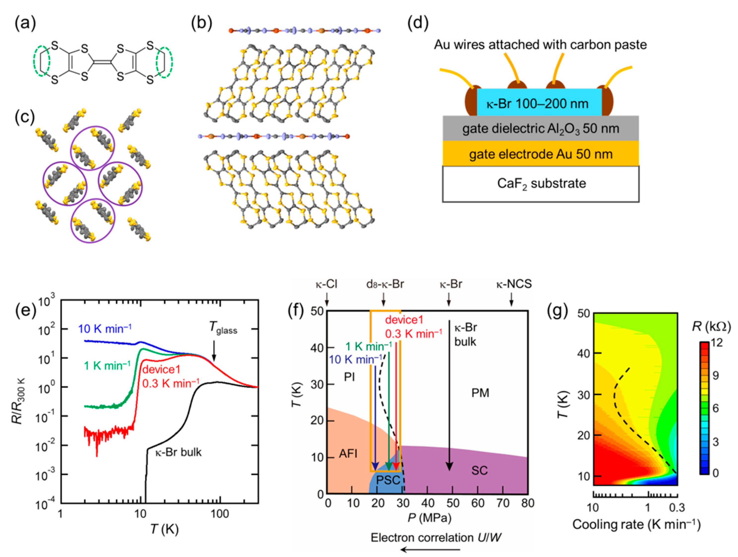
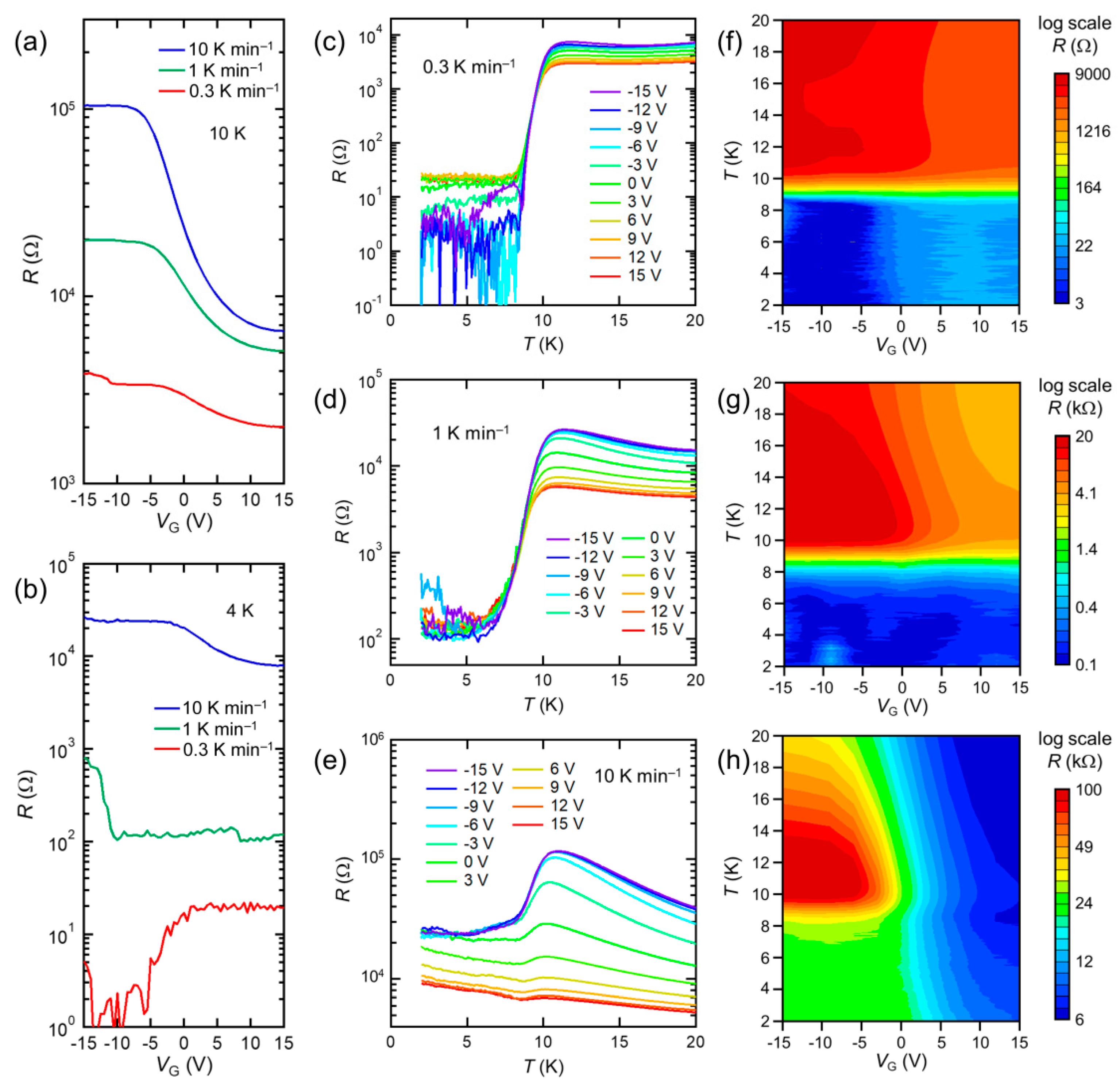
2. Results and Discussion

We laminated a κ-Br thin crystal on an Al2O3/Au/CaF2 substrate to fine-tune its bandwidth in the vicinity of insulator-to-superconductor transition by considering the thermal expansion coefficients α for κ-Br [23] and CaF2. Because the thin (~ 100–200 nm) κ-Br crystal is tightly bound on the substrate by van der Waals or dipole–dipole interactions, its lattice contraction is governed by that of the substrate. When the α value of the substrate is smaller than that of κ-Br, 2D negative pressure is effectively applied to the κ-Br during the cooling process [5]. In order to make moderate negative pressure, we utilized a CaF2 substrate which has larger α value compared to the substrates previously used to obtain the Mott insulating ground state of κ-Br (Table S1) [5,6,7,10,12,13].
The temperature dependence of resistance for a FET using thin κ-Br crystal on Al2O3/Au/CaF2 substrate (only that of device1) is shown in Figure 1e, where the data for both bulk κ-Br and device1 with various cooling rates are indicated. Though κ-Br is an organic superconductor with TC = 12 K [4], the thin crystal laminated onto the inorganic substrate becomes an insulator at low temperature by tensile strain from the substrate. Insulating nature becomes prominent with faster cooling rate. However, device1 did not show monotonic insulating behavior but showed incomplete SC transition with non-zero residual resistance below TC ~ 9 K. It suggests the percolative SC (PSC) state, where phase-separated SC and Mott insulating domains coexist in the vicinity of first-order pressure-induced Mott transition [18].
To consider the low-temperature state of device1 more carefully, a pressure–temperature (PT) phase diagram of κ-BEDT-TTF salts is presented in Figure 1f [3,24,25]. It is believed that κ-Br, κ-Cl, and κ-(BEDT-TTF)2Cu(NCS)2 (κ-NCS) can be mapped in an identical PT diagram with chemical pressure difference. The cooling trajectories of device1 with 0.3 K min−1, 1 K min−1, and 10 K min−1 cooling rates can be speculated (Figure 1e) as indicated by red, green, and blue arrows, respectively. The metal–insulator transition (or upturn of the resistance) around 15 K suggests that device1 has the electronic state on the border of Mott transition. We also note that magnetic field suppressed the partial SC transition, and an insulating nature of normal state became apparent (Figure S1).
The resistance difference due to the cooling rate control is seen below ca. 80 K, which is confirmed to be reproducible using different samples (device2, device3 in Figure S2). Similar significant cooling-rate dependence of resistivity has been reported in the partially deuterated κ-Br on the border of bandwidth-driven Mott transition, attributed to the glass transition of terminal ethylene group of BEDT-TTF molecule at ~80 K (Figure 1a) [26,27,28]. The glass transition refers to the freezing of vibration modes of BEDT-TTF terminal ethylene group, where the configuration of two ethylene end groups in BEDT-TTF aligns parallel (eclipsed) or canted (staggered) [22]. In κ-Br, the eclipsed configuration is energetically preferred, but more rapid cooling is considered to increase the population of the staggered configuration [29]. This conformational disorder is suggested to narrow the bandwidth by a theoretical study [30], providing one possible explanation for negative pressure effect by rapid cooling. In addition, the anisotropic changes of lattice parameters at glass transition are affected by cooling rate [22], which might play a role in the narrowing of the bandwidth upon rapid cooling [18]. In order to clarify the negative pressure effect by varying cooling rate, we display a color plot of resistance of device1 against cooling rate and temperature, and it is compared with PT phase diagram near the Mott transition (orange frame in Figure 1g). Although the low-temperature region below 8 K is difficult to describe due to limited data points, the insulator–metal phase boundary and PSC phase in the PT phase diagram are well reproduced in the color plot. It demonstrates that increasing cooling rate effectively produces negative pressure in device1.
We also note that disorder introduction into strongly correlated system can often induce Anderson localization [31]. It has been reported that continuous X-ray irradiation into κ-type BEDT-TTF salt causes structural defects in anion layers, leading to dramatic conductivity changes attributed to Anderson localization [32]. X-ray irradiation onto Mott-insulator such as κ-Cl decreases resistance because of softening of Coulomb gap. In the present result, however, we found only increase of resistance by rapid cooling (device3 in Figure S2b, for example). Therefore, a disorder effect or Anderson localization is not likely to be a primary cause for the resistance changes in our device.
Now we show the results of field-effect measurements in device1. Figure 2a is a summary of the gate voltage VG dependence of resistance at 10 K, just above TC, at different cooling rates. The resistance was decreased with increasing VG, indicating n-type FET operations. The monotonic n-type behavior in device1 suggests that the initial state (VG = 0 V) is slightly negatively charged compared to the half-filled state. Such a situation is often the case with κ-Br FET, the Fermi level of which interface seems to be located just below the upper Hubbard band [5,6,7]. The ON/OFF ratio remarkably increased by rapid cooling, which can be attributed to the enhancement of Mott insulating nature. Furthermore, we found strong influence of cooling rate on the field effect below TC in device1. Figure 2b shows the VG dependence of resistance at 4 K with different cooling rates, indicating a clear polarity change from n-type to p-type with decreasing cooling rate. The reproducibility of the results was confirmed with different samples (device3 in Figure S3, device4 in Figure S4).
In order to interpret this strange field effect below TC, the temperature dependence of logarithmic resistance below 20 K at fixed VG with the cooling rates of 0.3, 1, and 10 K min−1 are plotted in Figure 2c–e, respectively. It is found that the p-type field effect was only observed below TC at cooling rate of 0.3 K min−1 (Figure 2c). At 1 K min−1, VG dependence of the resistance was not large below TC (Figure 2d), and only n-type behavior was observed in whole temperature range at 10 K min−1 (Figure 2e).
For further discussion, contour maps were depicted in Figure 2f–h, which corresponds to the datasets of Figure 2c–e, respectively. In Figure 2f, very low resistance state was observed in the region with VG < 0 V and T < 8 K, as indicated by deep blue color. Because this deep blue region shrunk under magnetic field (Figure S5), the p-type behavior is considered to be derived from the enhancement of superconductivity at negative VG range. In the similar VGT region (VG < 0 V and T < 8 K), high resistance derived from Mott insulating state was observed in Figure 2h, as shown in the green region. These results indicate the enhancement of superconductivity in Figure 2f is observed at exactly half-filled state.
We display the schematic electronic phase diagram of κ-BEDT-TTF-based FET against electron correlation and band-filling at fixed temperature well below TC (Figure 3a), constructed from our previous experiments [10,15]. Considering the present field-effect measurements in device1 at different cooling rates, we present a revised version of this FET phase diagram in the vicinity of bandwidth-controlled Mott transition, as shown in Figure 3b. A novel finding is the particular enhancement of superconductivity at half filling observed at cooling rate of 0.3 K min−1, which is indicated by reddish violet region. Taking into account that the carrier doping here is very small (~a few % of band-filling) and takes place only at the first monolayer at FET interface [15], the current superconductivity enhancement should be difficult to understand in terms of the electron–phonon scattering [33] or the peculiar charge ordered state observed in cuprates [34]. At this stage, the mechanism behind this strange SC transition is an open question owing to the lack of appropriate experimental methods or theories.

3. Materials and Methods

Device Fabrication. Gold layer (50 nm) was deposited onto CaF2 substrate (Pure Optics, Tatebayashi, Japan) by DC magnetron sputtering (Quorum technologies, East Sussex, U.K.) for gate electrode. Alumina gate dielectric layer (50 nm) was fabricated by RF magnetron sputtering (Cryovac, Osaka, Japan) and/or atomic layer deposition (ALD; Picosun, Espoo, Finland). When using the sputtered (non-ALD) alumina layer, self-assembled monolayer (SAM) modification of the alumina surface using octadecylphosphonic acid (ODPA) was performed in order to reduce gate leakage current [35]. We synthesized a thin (~100–200 nm) κ-Br single crystal and laminated it onto the freshly prepared substrate as previously reported [10].
Measurements. Gold wires were attached to the κ-Br channel by carbon paste for conductivity measurement. Resistance was measured by conventional DC four-probe method (Keithley instruments, Solon, U.S.A.) under helium atmosphere in PPMS (Physical Property Measurement System; Quantum Design, San Diego, U.S.A.). Cooling rate was changed below 100 K, which is well above the glass transition temperature (~80 K) of terminal ethylene group of BEDT-TTF in κ-Br [22]. Magnetic field was applied perpendicular to the conducting plane.

4. Conclusions

A novel organic SC FET in the vicinity of bandwidth-controlled Mott transition has been developed using strongly correlated electron system κ-Br. We used CaF2 substrate for the first time, which has a slightly smaller thermal expansion coefficient than κ-Br, in order to fine-tune the bandwidth of κ-Br in FET structure. We succeeded in controlling the FET characteristics such as ON/OFF ratio and field-effect polarity by fine-tuning the bandwidth via cooling rate at glass transition of ethylene end groups of BEDT-TTF molecule. We found that the superconductivity is particularly stabilized at exactly half-filled state, which had not been known in κ-BEDT-TTF-based FET.

Supplementary Materials

The following are available online at https://www.mdpi.com/2073-4352/9/11/605/s1, Table S1: Thermal expansion coefficients α of substrate materials and κ-Br at room temperature, Figure S1: Low-temperature resistance of device1 under magnetic field, Figure S2: Temperature dependence of resistance in device2 (a) and device3 (b) at different cooling rate, Figure S3: Cooling-rate dependence of low-temperature resistance (a) and FET properties above TC (b) and below TC (c) in device3, Figure S4: Cooling-rate dependence of low-temperature resistance (a) and FET properties above TC (b) and below TC (c)–(e) in device4, Figure S5: Color plots of resistance of device1 below 12 K against VG and temperature at cooling rates of 0.3 K min−1 at 0 T (left) and 1 T (right).

Author Contributions

H.M.Y. designed the project. G.K. prepared the samples and performed the measurements. G.K. and H.M.Y. interpreted the data and wrote the manuscript.

Funding

This work was partly funded by Grant-in-Aid for Early-Career Scientists (No. 19K15526), Grant-in-Aid for Scientific Research (A) (No. 19H00891), (B) (No. 16H04140), (S) (No. 16H06346) from the Japan Society for the Promotion of Science (JSPS) and by JST ERATO Grant No. JPMJER1301, Japan.

Acknowledgments

A part of this work was conducted in Equipment Development Center (Institute for Molecular Science) and Hokkaido University, supported by Nanotechnology Platform Program of the Ministry of Education, Culture, Sport, Science and Technology (MEXT), Japan.

Conflicts of Interest

The authors declare no conflict of interest.

References

  1. Kanoda, K. Recent progress in NMR studies on organic conductors. Hyperfine Interact. 1997, 104, 235–249. [Google Scholar] [CrossRef]
  2. McKenzie, R.H. Similarities between organic and cuprate superconductors. Science 1997, 278, 820–821. [Google Scholar] [CrossRef]
  3. Ito, H.; Ishiguro, T.; Kubota, M.; Saito, G. Metal-nonmetal transition and superconductivity localization in the two-dimensional conductor κ-(BEDT-TTF)2Cu[N(CN)2]Cl under pressure. J. Phys. Soc. Jpn. 1996, 65, 2987. [Google Scholar] [CrossRef]
  4. Kini, A.M.; Geiser, U.; Wang, H.H.; Carlson, K.D.; Williams, J.M.; Kwok, W.K.; Vandervoort, K.G.; Thompson, J.E.; Stupka, D.L.; Jung, D.; et al. A new ambient-pressure organic superconductor, κ-(ET)2Cu[N(CN)2]Br, with the highest transition temperature yet observed (inductive onset TC = 11.6 K, resistive onset = 12.5 K). Inorg. Chem. 1990, 29, 2555–2557. [Google Scholar] [CrossRef]
  5. Kawasugi, Y.; Yamamoto, H.M.; Hosoda, M.; Tajima, N.; Fukunaga, T.; Tsukagoshi, K.; Kato, R. Strain-induced superconductor/insulator transition and field effect in a thin single crystal of molecular conductor. Appl. Phys. Lett. 2008, 92, 243508. [Google Scholar] [CrossRef]
  6. Kawasugi, Y.; Yamamoto, H.M.; Tajima, N.; Fukunaga, T.; Tsukagoshi, K.; Kato, R. Field-induced carrier delocalization in the strain-induced Mott insulating state of an organic superconductor. Phys. Rev. Lett. 2009, 103, 116801. [Google Scholar] [CrossRef]
  7. Kawasugi, Y.; Yamamoto, H.M.; Tajima, N.; Fukunaga, T.; Tsukagoshi, K.; Kato, R. Electric-field-induced Mott transition in an organic molecular crystal. Phys. Rev. B 2011, 84, 125129. [Google Scholar] [CrossRef]
  8. Kawasugi, Y.; Seki, K.; Edagawa, Y.; Sato, Y.; Pu, J.; Takenobu, T.; Yunoki, S.; Yamamoto, H.M.; Kato, R. Electron–hole doping asymmetry of Fermi surface reconstructed in a simple Mott insulator. Nat. Commun. 2016, 7, 12356. [Google Scholar] [CrossRef]
  9. Sato, Y.; Kawasugi, Y.; Suda, M.; Yamamoto, H.M.; Kato, R. Critical behavior in doping-driven metal–insulator transition on single-crystalline organic Mott-FET. Nano Lett. 2017, 17, 708–714. [Google Scholar] [CrossRef]
  10. Yamamoto, H.M.; Nakano, M.; Suda, M.; Iwasa, Y.; Kawasaki, M.; Kato, R. A strained organic field-effect transistor with a gate-tunable superconducting channel. Nat. Commun. 2013, 4, 2379. [Google Scholar] [CrossRef]
  11. Suda, M.; Kawasugi, Y.; Minari, T.; Tsukagoshi, K.; Kato, R.; Yamamoto, H.M. Strain-tunable superconducting field-effect transistor with an organic strongly-correlated electron system. Adv. Mater. 2014, 26, 3490–3495. [Google Scholar] [CrossRef] [PubMed]
  12. Suda, M.; Kato, R.; Yamamoto, H.M. Light-induced superconductivity using a photoactive electric double layer. Science 2015, 347, 743–746. [Google Scholar] [CrossRef] [PubMed]
  13. Suda, M.; Takashina, N.; Namuangruk, S.; Kungwan, N.; Sakurai, H.; Yamamoto, H.M. N-type superconductivity in an organic Mott insulator induced by light-driven electron-doping. Adv. Mater. 2017, 29, 1606833. [Google Scholar] [CrossRef] [PubMed]
  14. Kawaguchi, G.; Bardin, A.A.; Suda, M.; Uruichi, M.; Yamamoto, H.M. An Ambipolar Superconducting Field-Effect Transistor Operating above Liquid Helium Temperature. Adv. Mater. 2019, 31, 01805715. [Google Scholar] [CrossRef] [PubMed]
  15. Kawasugi, Y.; Seki, K.; Tajima, S.; Pu, J.; Takenobu, T.; Yunoki, S.; Yamamoto, H.M.; Kato, R. Two-dimensional ground-state mapping of a Mott–Hubbard system in a flexible field-effect device. Sci. Adv. 2019, 5, eaav7282. [Google Scholar] [CrossRef]
  16. Suda, M.; Yamamoto, H.M. Field-, strain- and light-induced superconductivity in organic strongly correlated electron systems. Phys. Chem. Chem. Phys. 2018, 20, 1321–1331. [Google Scholar] [CrossRef]
  17. Yamamoto, H.M.; Suda, M.; Kawasugi, Y. Organic phase-transition transistor with strongly correlated electrons. Jpn. J. Appl. Phys. 2018, 57, 03EA02. [Google Scholar] [CrossRef]
  18. Sasaki, T.; Yoneyama, N.; Suzuki, A.; Kobayashi, N.; Ikemoto, Y.; Kimura, H. Real space imaging of the metal–insulator phase separation in the band width controlled organic Mott system κ-(BEDT-TTF)2Cu[N(CN)2]Br. J. Phys. Soc. Jpn. 2005, 74, 2351–2360. [Google Scholar] [CrossRef]
  19. Kawamoto, A.; Miyagawa, K.; Kanoda, K. Deuterated κ-(BEDT-TTF)2Cu[N(CN)2]Br: A system on the border of the superconductor–magnetic-insulator transition. Phys. Rev. B 1997, 55, 14140. [Google Scholar] [CrossRef]
  20. Su, X.; Zuo, F.; Schlueter, J.A.; Kelly, M.E.; Williams, J.M. Structural disorder and its effect on the superconducting transition temperature in the organic superconductor κ-(BEDT-TTF)2Cu[N(CN)2]Br. Phys. Rev. B 1998, 57, R14056. [Google Scholar] [CrossRef]
  21. Su, X.; Zuo, F.; Schlueter, J.A.; Kini, A.M.; Williams, J.M. 80 K anomaly and its effect on the superconducting and magnetic transition in deuterated κ-(BEDT-TTF)2Cu[N(CN)2]Br. Phys. Rev. B 1998, 58, R2944. [Google Scholar] [CrossRef]
  22. Müller, J.; Lang, M.; Steglich, F.; Schlueter, J.A.; Kini, A.M.; Sasaki, T. Evidence for structural and electronic instabilities at intermediate temperatures in κ-(BEDT-TTF)2X for X=Cu[N(CN)2]Cl, Cu[N(CN)2]Br and Cu(NCS)2: Implications for the phase diagram of these quasi-two-dimensional organic superconductors. Phys. Rev. B 2002, 65, 144521. [Google Scholar] [CrossRef]
  23. Kund, M.; Muller, H.; Biberacher, W.; Andres, K.; Saito, G. Anomalous thermal expansion of the organic superconductor κ-(BEDT-TTF)2Cu[N(CN)2]Br. Phys. B Condens. Matter 1993, 191, 274–280. [Google Scholar] [CrossRef]
  24. Kagawa, F.; Itou, T.; Miyagawa, K.; Kanoda, K. Transport criticality of the first-order Mott transition in the quasi-two-dimensional organic conductor κ-(BEDT-TTF)2Cu[N(CN)2]Cl. Phys. Rev. B 2004, 69, 064511. [Google Scholar] [CrossRef]
  25. Powell, B.J.; McKenzie, R.H. Half-filled layered organic superconductors and the resonating-valence-bond theory of the Hubbard-Heisenberg model. Phys. Rev. Lett. 2005, 94, 047004. [Google Scholar] [CrossRef] [PubMed]
  26. Taniguchi, H.; Kawamoto, A.; Kanoda, K. Superconductor-insulator phase transformation of partially deuterated κ-(BEDT-TTF)2Cu[N(CN)2]Br by control of the cooling rate. Phys. Rev. B 1999, 59, 8424. [Google Scholar] [CrossRef]
  27. Taniguchi, H.; Kanoda, K.; Kawamoto, A. Field switching of superconductor-insulator bistability in artificially tuned organics. Phys. Rev. B 2003, 67, 014510. [Google Scholar] [CrossRef]
  28. Hartmann, B.; Müller, J.; Sasaki, T. Mott metal-insulator transition induced by utilizing a glasslike structural ordering in low-dimensional molecular conductors. Phys. Rev. B 2014, 90, 195150. [Google Scholar] [CrossRef]
  29. Ishiguro, T.; Yamaji, K.; Saito, G. Organic Superconductors, 2nd ed.; Springer: Berlin/Heidelberg, Germany, 1998. [Google Scholar]
  30. Guterding, D.; Valentí, R.; Jeschke, H.O. Influence of molecular conformations on the electronic structure of organic charge transfer salts. Phys. Rev. B 2015, 92, 081109. [Google Scholar] [CrossRef]
  31. Anderson, P.W. Absence of diffusion in certain random lattices. Phys. Rev. 1958, 109, 1492–1505. [Google Scholar] [CrossRef]
  32. Sasaki, T. Mott-Anderson Transition in Molecular Conductors: Influence of Randomness on Strongly Correlated Electrons in the κ-(BEDT-TTF)2X System. Crystals 2012, 2, 374–392. [Google Scholar] [CrossRef]
  33. Abdel-Jawad, M.; Kennett, M.P.; Balicas, L.; Carrington, A.; Mackenzie, A.P.; McKenzie, R.H.; Hussy, N.E. Anisotropic scattering and anomalous normal-state transport in a high-temperature superconductor. Nat. Phys. 2006, 2, 821–825. [Google Scholar] [CrossRef] [Green Version]
  34. da Silva Neto, E.H.; Aynajian, P.; Frano, A.; Comin, R.; Schierle, E.; Weschke, E.; Gyenis, A.; Wen, J.; Schneeloch, J.; Xu, Z.; et al. Ubiquitous interplay between charge ordering and high-temperature superconductivity in cuprates. Science 2014, 343, 393–396. [Google Scholar] [CrossRef] [PubMed] [Green Version]
  35. Klauk, H.; Zschieschang, U.; Pflaum, J.; Halik, M. Ultralow-power organic complementary circuits. Nature 2007, 445, 745. [Google Scholar] [CrossRef] [PubMed]
Figure 1. (a) BEDT-TTF molecule. The part surrounded by dotted line is terminal ethylene group. (b) Side view of crystal structure of κ-Br. Two-dimensional BEDT-TTF layer and insulating anion layer are alternating. (c) BEDT-TTF layer viewed along the long axis of BEDT-TTF molecule. Purple circle shows the dimer. (d) Device structure of a novel FET using κ-Br. (e) Temperature dependence of resistance of device1 at cooling rate of 0.3, 1, and 10 K min−1 and bulk κ-Br. Resistance is normalized by the resistance value at 300 K for clarity. Glass transition temperature of terminal ethylene groups is shown by Tglass. (f) PT phase diagram of κ-BEDT-TTF salts, constructed by previous reports [3,24,25]. Bottom and top axes indicate physical pressure relative to ambient-pressure state of κ-Cl and chemical pressure by anion variation, respectively. Decreasing pressure P strengthens the electron correlation U/W, where U and W represent on-site Coulomb repulsion and bandwidth, respectively. d8-κ-Br represents fully deuterated κ-Br. PI, PM, AFI, SC, and PSC denote paramagnetic insulator, paramagnetic metal, antiferromagnetic insulator, superconductor, and percolative superconductor, respectively. Red, green, blue, and black arrows indicate the cooling trajectories of device1 at the cooling rate of 0.3, 1, 10 K min−1, and κ-Br bulk, respectively, expected from the data in Figure 1e. Orange box indicates the parameter region measured in 1e. (g) Color plot of resistance against cooling rate and temperature of device1, which is comparable to the region surrounded by orange frame in Figure 1f. The S-shaped phase boundary between PI and PM seems to be reproduced as shown by broken curve.
Crystals 09 00605 g001
Figure 2. Gate voltage VG dependence of resistance of device1 at 10 K (a) and 4 K (b) with different cooling rates. Temperature dependence of resistance of device1 below 20 K under various VG at cooling rates of 0.3 K min−1 (c), 1 K min−1 (d), and 10 K min−1 (e). Color plots of resistance below 20 K against VG and temperature at cooling rates of 0.3 K min−1 (f), 1 K min−1 (g), and 10 K min−1 (h).
Crystals 09 00605 g002
Figure 3. (a) Schematic phase diagram of κ-BEDT-TTF salts around Mott insulator against electron correlation and band-filling at fixed temperature well below TC [10,15]. Half-filled state is emphasized with highlight. Here PSC phase is omitted for simplicity. (b) Expanded figure of the region surrounded by broken line in Figure 3a and the field effects in device1 at different cooling rates. Double-headed arrows indicate observed ranges. Reddish violet region indicates SC state stabilized at half filling that we newly found here.
Crystals 09 00605 g003

