Commentary

A Fundamental Reason for the Need of Two Different Semiconductor Technologies for Complementary Thin-Film Transistor Operations

Department of Electronics, Pusan National University, Pusan 46241, Korea
*
Author to whom correspondence should be addressed.
Crystals 2019, 9(11), 603; https://doi.org/10.3390/cryst9110603
Submission received: 8 November 2019 / Revised: 14 November 2019 / Accepted: 15 November 2019 / Published: 17 November 2019
(This article belongs to the Special Issue Advances in Thin Film Materials and Devices)

Abstract

:
In this short commentary, we discuss a fundamental reason why two different semiconductor technologies are needed for complementary thin-film transistor (TFT) operations. It is mainly related to an energy-level matching between the band edge of the semiconductor and the work-function energy of the metal, which is used for the source and drain electrodes. The reference energy level is determined by the energy range of work-functions of typical metals for the source and drain electrodes. With the exception of silicon, both the conduction band edge (EC) and valence band edge (EV) of a single organic or inorganic material are unlikely to match the metal work-function energy whose range is typically from −4 to −6 eV. For example, typical inorganic materials, e.g., Zn–O, have the EC of around −4.5 eV (i.e., electron affinity), so the conduction band edge is within the range of the metal work-function energy, suggesting its suitability for n-channel TFTs. On the other hand, p-type inorganic materials, such as Cu–O, have an EV of around −5.5 eV, so the valence band edge is aligned with metal work-function energy, thus the usage for p-channel TFTs. In the case of p-type and n-type organic materials, their highest occupied molecular orbital (HOMO) and lowest occupied molecular orbital (LUMO) should be aligned with metal work-function energy. For example, p-type organic material, e.g., pentacene, has a HOMO level around −5 eV, which is within the range of the metal work-function energy, implying usage for p-channel TFTs. However, its LUMO level is around −3 eV, not being aligned with the metals’ work-function energy. So it is hard to use pentacene for n-channel TFTs. Along with this, n-type organic materials (e.g., C60) should have HOMO levels within the typical metals’ work-function energy for the usage of n-channel TFT. To support this, we provide a qualitative and comparative study on electronic material properties, such as the electron affinity and band-gap of representative organic and inorganic materials, and the work-function energy of typical metals.

1. Introduction

Complementary metal-oxide-semiconductor (CMOS) technology is a mature and traditional device technology, especially for non-display applications [1]. Here, the single type of the semiconductor, which is silicon, can be employed for both n-channel and p-channel metal-oxide-semiconductor field-effect transistors (MOSFETs), and thus the CMOS operation. This is possible because silicon has proper energy-band properties in terms of a band-gap (~1.1 eV) and conduction band minimum energy (i.e., an electron affinity of −4.05 eV), and thus a valence band maximum energy of 5.15 eV [2]. Additionally, these unique properties allow both electron conduction for n-channel devices and hole conduction for p-channel devices through the metal electrodes where these carriers are collected by minimizing rectification and interference. In other words, it can fit various metals with different work-function energies whose range are typically form −4 to −6 eV [3]. Essentially, the conduction band minimum (EC) and valence band maximum (EV) of silicon are within this work-function energy range of typically available metals.
However, CMOS technology has shortcomings when it comes to flexible/transparent electronics. Due to the necessity of a high-temperature process for CMOS technology, using flexible/transparent substrate (e.g., plastic) with low melting-points is almost impossible. So, to build electronic circuits on those substrates for transparent electronic systems or wearable devices, thin-film transistors (TFTs) based on room-temperature-processable or solution-processable non-silicon semiconductors (such as organic semiconductors and inorganic semiconductors represented by metal oxides) have been studied [4,5,6,7,8]. Different from display applications, both n-type and p-type transistors are necessary for performing complex functions and constitute circuit blocks. Unfortunately, unlike silicon, neither organic materials or inorganic materials are solely usable for both n-channel and p-channel thin-film transistors (TFTs) [9]. For instance, it is known that n-type inorganic and organic semiconductors, e.g., Zn-O and C60 are more favorable for electron transport, suggesting it for the n-channel TFTs. In contrast, p-type inorganic and organic materials, such as Cu-O and pentacene, better for the hole transport, are employed for p-channel TFTs. This implies that the conduction band of these n-type materials is only used for electrons while the valence band of p-type materials is only available for holes. Since the carrier transport within the semiconductor starts and ends at the metal electrodes at the source and drain, respectively, the metal property, e.g., work-function energy, should be associated with the TFT operation in terms of the type of main transport carrier. This technological issue of non-silicon-based TFTs is to be explained from a more fundamental point of view. In this paper, we present a theoretical discussion on a fundamental reason why two different semiconductor technologies should be employed for complementary TFT operations. It is mainly associated with an energy-level alignment between the band edge of the semiconductor and work-function energy of the metal incorporated as the source or drain electrode where the main transport carrier (e.g., electrons or holes) is supplied or collected. This suggests that both the conduction band minimum and valence band maximum of a single organic or inorganic material are unlikely to fit the work-function energy of typical metals. As the electron conduction material, n-type inorganic materials, e.g. Zn-O, have a high EC and a very low EV due to the wide band-gap. Here, EC is only within the range of the available metal’s work-function energy, so the conduction band edge can only be aligned with the metal electrode, suggesting its suitability as n-channel TFTs. Additionally, for n-type organic materials, e.g., C60, its EC (i.e., lowest occupied molecular orbital, LUMO) is aligned with the metal work-function energy level, having n-rich material property. So this can be used for n-channel TFTs. In contrast to this, p-type organic semiconductors have a high EV (i.e., highest occupied molecular orbital, HOMO), which is within the range of the metal work-function energy, so they are suitable for p-channel TFTs. Along with this, p-type inorganic materials, such as Sn-O, have an energy band whose EV is only matched with a metal’s work-function energy, thus a possibility of p-channel material. These imply that a complementary TFT operation is possible from a combination of these two different material families. Regarding these theoretical insights, we show a qualitative and comparative study on electronic material properties of some organic and inorganic materials and the work-function energy of some of the metals typically used in TFTs.

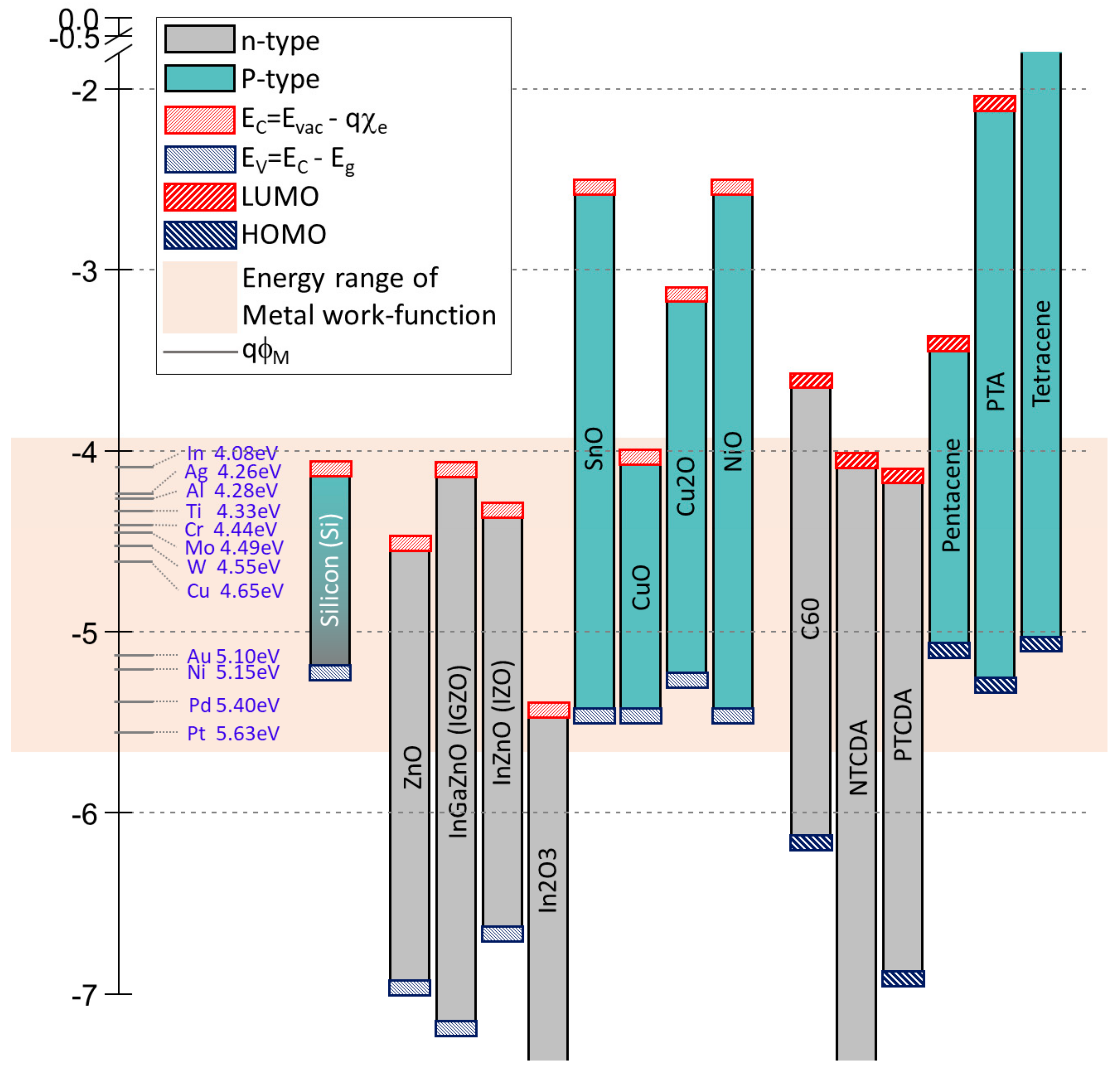
2. Comparative Table of Electronic Material Properties

Figure 1 shows a comparative table of basic electronic properties of inorganic materials, organic materials, and metals, While the inorganic or organic semiconductor materials are used as the channel layer in TFT structures, metals are used as the electrode at the source and drain terminals where the conduction path starts or ends through the semiconductor channel layer, providing the terminal current modulated with the insulated gate capacitor structure [10]. This section mainly focuses on these channel materials and metals in the TFT structure.

2.1. n-Type Inorganic Materials

As can be seen in Figure 1, firstly, n-type inorganic materials, represented by conducting oxides (e.g., Zn-O [11]), have a high electron affinity (χe) around −4.5 eV [12]. This determines the energy level of the conduction band minimum. Besides, due to the wide band-gap (Eg) of more than 3 eV [13], the valence band maximum is very low at around −7 eV measured from the vacuum energy (Evac). Since the work-function energy of typical metals is within the range from −4 to −6 eV, only the conduction band edge of n-type inorganic materials is aligned with the metal which is used for an electrode in TFT structures.

2.2. p-Type Inorganic Materials

P-type inorganic materials, such as Ni-O and Sn-O, have an EV of around −5.5 eV and an EC of around −2.5 eV [14,15], as shown in Figure 1. Since their EV are within the range from −4 to −6 eV and their EC are out of the range of typical metal, the valence band edge of p-type inorganic materials is only aligned with typical metals.
As can be seen in Figure 1, Cu-O has an EV of around −5.5 eV, and an EC of around −4 eV [16]. In this case, both EC and EV are within the range of typical metal’s work-function energy, so it seems that it can be used for both n-channel and p-channel TFTs’ channel material. However, due to its material nature (e.g., high vacancy formation enthalpy, high degree of disorder near EC), oxygen interstitials and copper vacancies contribute to a p-type conductivity, thus making it a p-type material [17,18].

2.3. p-Type Organic Materials

As shown in Figure 1, the HOMO level, equivalent to EV, of typical p-type organic materials (e.g., pentacene) are around −5 eV from Evac. However, the LUMO as EC is located at around −3 eV, which is closer to Evac by the amount of energy of Eg [19]. So, these properties make the HOMO level only aligned with the work-function energy of typical metals (i.e., ϕm from 4 to 6 eV).

2.4. n-Type Organic Materials

In contrast to the p-type organic materials, n-type organic materials’ EV (i.e., LUMO) is aligned with the work-function of the typical metals. As can be seen in Figure 1, n-type organic material C60 has LUMO level of −3.5 eV and HOMO level of −6.2 eV [20]. Besides, though both LUMO and HOMO can be aligned with each metal, p-type doping of C60 is difficult because of its high ionization energy [21]. So it can be used only for n-channel TFTs with proper doping.

2.5. Metals

As another key element in TFTs, metals are used as the source and drain electrodes where the carriers, e.g., electrons and holes, are collected forming the terminal current between the drain and source. As seen in Figure 1, the work-function energy of typical metals (e.g., In, Ag, Al, Ti, Cr, Mo, W, Cu, Au, Ni, Pd, Pt) are largely within the range of −4 to −6 eV. These metals have relatively high electrical strength and electronic stability in terms of bonding across the metal molecules, thus a low reactivity with an ambient condition. This suggests that these metals are stable enough to be used as the terminal electrodes. Note that there is an exception, i.e., sodium (Na), with work-function energy around −2.3 eV, which is too unstable and reactive to be used as the transistor’s terminal electrode.

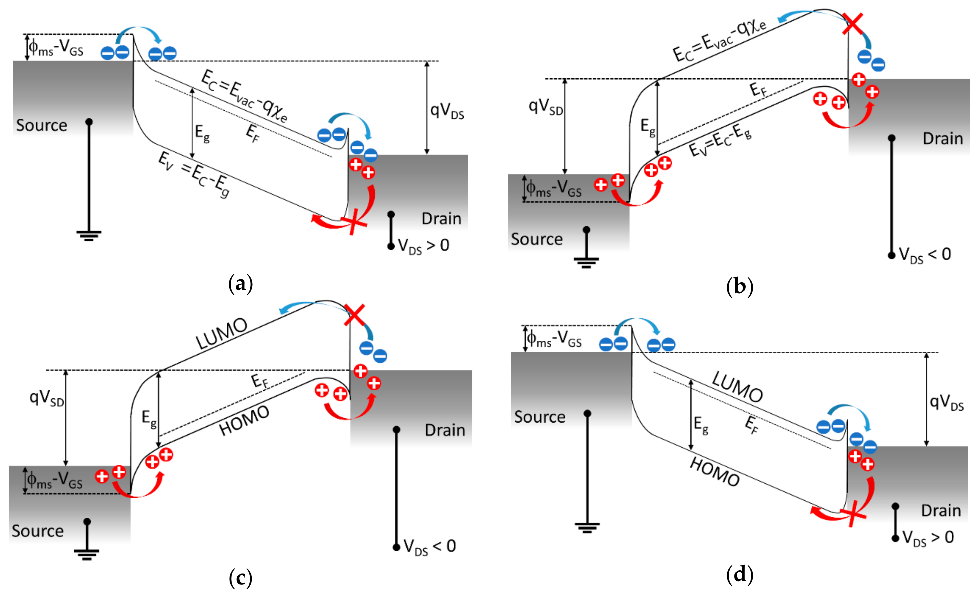
3. Carrier Transport through Semiconductors and Metals in TFTs

3.1. Electron Transport and n-Type Inorganic Materials with Metals

As discussed in the previous Section 2.1, the conduction band edge of n-type inorganic semiconductors is well aligned with the work-function energy of typical metals. This means that electron transport can be well established, especially with a n-type inorganic material. Figure 2a shows a horizontal band diagram along the channel length from the source to the drain. As seen here, electrons are supplied from the source metal, and travel through an inorganic material. Finally, they are collected at the drain metal, forming the terminal current. Here, it is noticed that the barrier height between the work-function energy level of the drain metal and EV of the channel layer is too high to get the hole transport. So, a very high Schottky barrier height for holes exists, making this kind of semiconductor materials not suitable for p-channel (i.e., hole conduction) TFTs.
Besides, a degree of disorder of the conduction band in inorganic semiconductors is very low; thus, a Fermi level can be easily modulated by the gate field in TFT structures [22], with no significant interference in the carrier transport [23]. In oxide-based inorganic materials, oxygen vacancies formed during the film deposition process play the role of the electron donner; thus, an n-type conducting oxide is controlled by the amount of oxygen vacancies [24,25].

3.2. Hole Transport and p-Type Inorganic Materials with Metals

For the usage for p-channel TFTs, p-type organic materials should have EV that is within the range of typical metal work-function energy, thus a hole transport. Figure 2b shows a horizontal band diagram of the source to the drain through the channel in the p-channel TFT. Holes supplied from the source are collected at the drain through the inorganic material. As we discussed in the previous section, Ni-O and Sn-O have a high Ev around −5.5 eV, matching the typical metal work-function energy range, thus a hole transport. Its low Ec around −2.5 eV, however, makes it hard for the electrons to travel, forming a high Schottky barrier. Here, it is clear that hole transport is well established through the pentacene, while electrons transport poorly.
Here, CuO has an EC and an EV that can both be aligned with typical metal work-function. From this point of view, it seems that both electron and hole conduction can be established. However, as discussed in the previous Section 2.2, due to its material nature, the number of free electrons is very small, thus a poor conductor for the electrons.
In this type of oxide semiconductors, sub-gap tail states near the conduction band, known to originate mainly from defects such as metal vacancy, contribute to the hole concentration. This also traps electrons, thus being a well-established hole transport and poor electron transport [26].

3.3. Hole Transport and p-Type Organic Materials with Metals

The valence band edge (i.e., HOMO) of p-type organic materials, e.g., typical polymers, is well-matched with the work-function energy of metals, as discussed in the previous Section 2.2. This suggests that the hole transport can be made. As seen in Figure 2c, the horizontal band diagram describes that holes are traveling from the source metal to the drain metal, and the intermediate medium is a p-type organic semiconductor. As can be seen, holes can overcome the barrier between the metal and EV (i.e., HOMO), while electrons face a high barrier height. Within the organic semiconductor, the number of holes are modulated by the position of the Fermi level externally controlled by the gate field. Note that the density of states for the valence band has a Gaussian profile where holes are hopping through [27].

3.4. Electron Transport and n-Type Organic Materials with Metals

In the n-type organic material case, the conduction band edge (i.e., LUMO) should be matched with the metal work-function energy. See Figure 2d for the horizontal band diagram of n-type organic channel TFT. Electrons are supplied from the source, traveling through the organic material, collected at the drain, thus forming terminal current. Along with other cases in this section, electrons easily overcome the barrier between the metal and semiconductor, while holes face high barriers, thus only the electrons transport. However, there are n-type organic materials whose HOMO and LUMO can both be matched with the metal work-function range, such as C60. Unfortunately, p-type doping of C60 film is difficult due to its high ionization energy.
Here, the main mechanism of electron transport in n-type organic material is hopping conduction [28]. Additionally, the charge-carrier states are disordered with a Gaussian profile. [29].

4. Summary

We have discussed a fundamental reason for the need of two different materials for a complementary operation of TFTs. There are several possible combinations, such as n-type and p-type organics [30], n-type and p-type inorganics [31], n-type inorganics and p-type organics [32,33], and n-type organics and p-type inorganics (even with the inefficient combination). Along with the limited range of metal work-functions, only one of the conduction band and valence band edges is aligned with the work-function energy level of typical metals. This essentially determines a suitability to be used as an n-channel or p-channel material regardless of whether it is an organic or inorganic material. Consequently, this work can be a good basis for the selection of materials and their combinations for an n-channel or p-channel TFT.

Author Contributions

S.L. did all the study and analysis provided here and J.J. and S.L. wrote the entire manuscript with an intensive discussion.

Acknowledgments

This research was supported by Basic Science Research Program through the National Research Foundation of Korea (NRF) funded by the Ministry of Science, ICT & Future Planning (NRF-2018R1C1B6001688).

Conflicts of Interest

The authors declare no conflict of interest.

References

  1. Weste, N.H.; Eshraghian, K. Principles of CMOS VLSI Design: A Systems Perspective; Addison-Wesley Publishing Company: Boston, MA, USA, 1993. [Google Scholar]
  2. Shur, M.S. Handbook Series on Semiconductor Parameters; World Scientific: Singapore, 1997. [Google Scholar]
  3. Robertson, J. Band offsets and work function control in field effect transistors. J. Vac. Sci. Technol. B 2009, 27, 277. [Google Scholar] [CrossRef]
  4. Zhang, L.; Xiao, W.; Wu, W.; Liu, B. Research progress on flexible oxide-based thin film transistors. Appl. Sci. 2019, 9, 773. [Google Scholar] [CrossRef]
  5. Nathan, A.; Ahnood, A.; Cole, M.T.; Lee, S.; Suzuki, Y.; Hiralal, P.; Bonaccorso, F.; Hasan, T.; Garcia-Gancedo, L.; Dyadyusha, A.; et al. Flexible electronics: The next ubiquitous platform. Proc. IEEE 2012, 100, 1486–1517. [Google Scholar] [CrossRef]
  6. Jang, J.; Kang, Y.; Cha, D.; Bae, J.; Lee, S. Thin-Film Optical Devices Based on Transparent Conducting Oxides: Physical Mechanisms and Applications. Crystals 2019, 9, 192. [Google Scholar] [CrossRef]
  7. Sun, B.; Sirringhaus, H. Solution-processed zinc oxide field-effect transistors based on self-assembly of colloidal nanorods. Nano Lett. 2005, 5, 2408–2413. [Google Scholar] [CrossRef] [PubMed]
  8. Xiao, P.; Huang, J.; Dong, T.; Xie, J.; Yuan, J.; Luo, D.; Liu, B. Room-temperature fabricated thin-film transistors based on compounds with lanthanum and main family element boron. Molecules 2018, 23, 1373. [Google Scholar] [CrossRef]
  9. Chen, H.; Cao, Y.; Zhang, J.; Zhou, C. Large-scale complementary macroelectronics using hybrid integration of carbon nanotubes and IGZO thin-film transistors. Nat. Commun. 2014, 5, 4097. [Google Scholar] [CrossRef]
  10. Weimer, P.K. The TFT a new thin-film transistor. Proc. IRE 1962, 50, 1462–1469. [Google Scholar] [CrossRef]
  11. Fortunato, E.M.C.; Barquinha, P.M.C.; Pimentel, A.C.M.B.G.; Gonçalves, A.M.F.; Marques, A.J.S.; Martins, R.F.P.; Pereira, L.M. Wide-bandgap high-mobility ZnO thin-film transistors produced at room temperature. Appl. Phys. Lett. 2004, 85, 2541. [Google Scholar] [CrossRef]
  12. Hussain, B.; Aslam, A.; Khan, T.M.; Creighton, M.; Zohuri, B. Electron affinity and bandgap optimization of zinc oxide for improved performance of ZnO/Si heterojunction solar cell using PC1D simulations. Electronics 2019, 8, 238. [Google Scholar] [CrossRef]
  13. Kohan, A.F.; Ceder, G.; Morgan, D.; Van De Walle, C.G. First-principles study of native point defects in ZnO. Phys. Rev. B 2000, 61, 15019–15027. [Google Scholar] [CrossRef]
  14. Afanas’Ev, V.V.; Badylevich, M.; Houssa, M.; Stesmans, A.; Aggrawal, G.; Campbell, S.A. Electron energy band alignment at the NiO/SiO2 interface. Appl. Phys. Lett. 2010, 96, 172105. [Google Scholar] [CrossRef]
  15. Scanlon, D.O.; Watson, G.W. On the possibility of p-type SnO2. J. Mater. Chem. 2012, 22, 25236–25245. [Google Scholar] [CrossRef]
  16. Koffyberg, F.P.; Benko, F.A. A photoelectrochemical determination of the position of the conduction and valence band edges ofp-type CuO. J. Appl. Phys. 1982, 53, 1173–1177. [Google Scholar] [CrossRef]
  17. Zhang, N.; Sun, J.; Gong, H. Transparent p-Type Semiconductors: Copper-Based Oxides and Oxychalcogenides. Coatings 2019, 9, 137. [Google Scholar] [CrossRef]
  18. Meyer, B.K.; Polity, A.; Reppin, D.; Becker, M.; Hering, P.; Klar, P.J.; Sander, T.; Reindl, C.; Benz, J.; Eickhoff, M.; et al. Binary copper oxide semiconductors: From materials towards devices. Phys. Status Solidi 2012, 249, 1487–1509. [Google Scholar] [CrossRef]
  19. Dong, H.; Wang, C.; Hu, W. High performance organic semiconductors for field-effect transistors. Chem. Commun. 2010, 46, 5211–5222. [Google Scholar] [CrossRef]
  20. Djurovich, P.I.; Mayo, E.I.; Forrest, S.R.; Thompson, M.E. Measurement of the lowest unoccupied molecular orbital energies of molecular organic semiconductors. Org. Electron. 2009, 10, 515–520. [Google Scholar] [CrossRef]
  21. Claves, D. Hole-doping of fullerenes and nanotubes by way of intercalation chemistry. J. Nanosci. Nanotechnol. 2007, 7, 1221–1238. [Google Scholar] [CrossRef]
  22. Lee, S.; Nathan, A. Conduction threshold in accumulation-mode InGaZnO thin film transistors. Sci. Rep. 2016, 6, 22567. [Google Scholar] [CrossRef]
  23. Lee, S.; Striakhilev, D.; Jeon, S.; Nathan, A. Unified analytic model for current–voltage behavior in amorphous oxide semiconductor TFTs. EEE Electron Device Lett. 2013, 35, 84–86. [Google Scholar] [CrossRef]
  24. Liu, H.; Zeng, F.; Lin, Y.; Wang, G.; Pan, F. Correlation of oxygen vacancy variations to band gap changes in epitaxial ZnO thin films. Appl. Phys. Lett. 2013, 102, 181908. [Google Scholar] [CrossRef]
  25. Chiu, C.; Pei, Z.; Chang, S.; Chang, S.; Chang, S. Effect of oxygen partial pressure on electrical characteristics of amorphous indium gallium zinc oxide thin-film transistors fabricated by thermal annealing. Vacuum 2011, 86, 246–249. [Google Scholar] [CrossRef]
  26. Isseroff, L.Y.; Carter, E.A. Electronic Structure of Pure and Doped Cuprous Oxide with Copper Vacancies: Suppression of Trap States. Chem. Mater. 2013, 25, 253–265. [Google Scholar] [CrossRef]
  27. Oehzelt, M.; Koch, N.; Heimel, G. Organic semiconductor density of states controls the energy level alignment at electrode interfaces. Nat. Commun. 2014, 5, 4174. [Google Scholar] [CrossRef]
  28. Kremer, R.K.; Rabenau, T.; Maser, W.K.; Kaiser, M.; Simon, A.; Haluska, M.; Kuzmany, H. High-temperature conductivity study on single-crystal C 60. Appl. Phys. A 1993, 56, 211–214. [Google Scholar] [CrossRef]
  29. Berkai, Z.; Daoudi, M.; Mendil, N.; Belghachi, A. Monte Carlo simulation of electric conductivity for pure and doping fullerene (C60). Phys. Lett. A 2019, 383, 2090–2092. [Google Scholar] [CrossRef]
  30. Gundlach, D.J.; Pernstich, K.P.; Wilckens, G.; Grüter, M.; Haas, S.; Batlogg, B. High mobility n-channel organic thin-film transistors and complementary inverters. J. Appl. Phys. 2005, 98, 064502. [Google Scholar] [CrossRef]
  31. Chiu, I.-C.; Li, Y.-S.; Tu, M.-S.; Cheng, I.-C. Complementary Oxide–Semiconductor-Based Circuits With n-Channel ZnO and p-Channel SnO Thin-Film Transistors. IEEE Electron. Device Lett. 2014, 35, 1263–1265. [Google Scholar] [CrossRef]
  32. Oh, M.S.; Hwang, D.K.; Lee, K.; Im, S.; Yi, S. Low voltage complementary thin-film transistor inverters with pentacene-ZnO hybrid channels on AlOx dielectric. Appl. Phys. Lett. 2007, 90. [Google Scholar] [CrossRef]
  33. Nomura, K.; Aoki, T.; Nakamura, K.; Kamiya, T.; Nakanishi, T.; Hasegawa, T.; Kimura, M.; Kawase, T.; Hirano, M.; Hosono, H. Three-dimensionally stacked flexible integrated circuit: Amorphous oxide/polymer hybrid complementary inverter using n-type a-In–Ga–Zn–O and p-type poly-(9,9-dioctylfluorene-co-bithiophene) thin-film transistors. Appl. Phys. Lett. 2010, 96. [Google Scholar] [CrossRef]
Figure 1. A graph compares energy band edge positions of n-type and p-type inorganic/organic semiconductor materials with a typical contact metal’s work-function energy.
Crystals 09 00603 g001
Figure 2. Energy band diagram along the channel from source to drain of the TFT, which is in on-state. (a) Inorganic n-channel TFT case with positive VGS and VDS. The electrons are traveling well while the holes are facing the high barrier. (b) Inorganic p-channel TFT case with negative VGS and VDS. The holes transport through the channel, but the electrons are blocked by the high barrier. (c) Organic p-channel TFT case with negative VGS and VDS. Only the hole conduction is established as well as the inorganic p-channel TFT case. (d) Organic n-channel TFT case with positive VGS and VDS. Only the electrons travel along the channel; likewise, the case of inorganic n-channel TFT.
Crystals 09 00603 g002

