Growth and Strain Engineering of Trigonal Te for Topological Quantum Phases in Non-Symmorphic Chiral Crystals

 ,
, 
Abstract
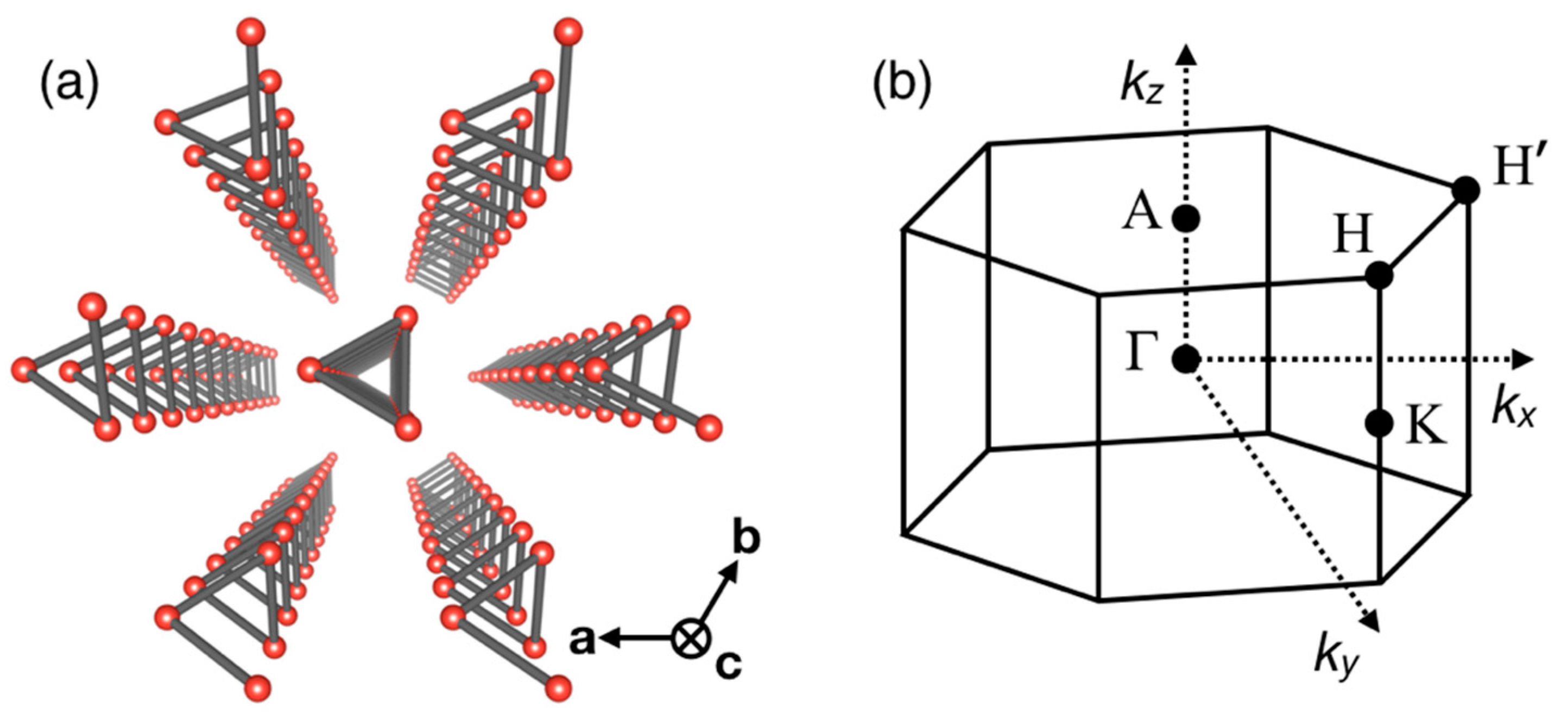
1. Introduction
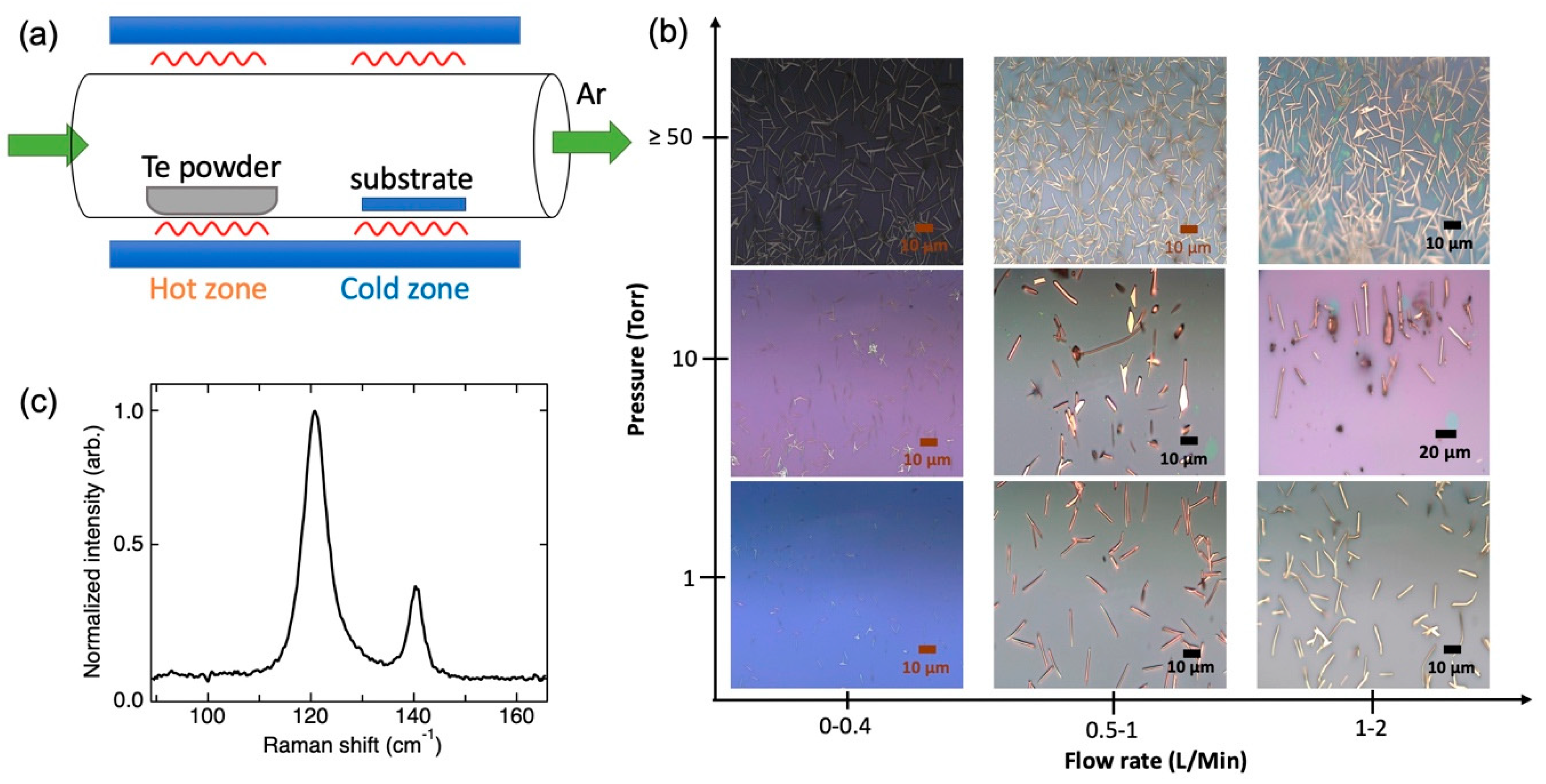
2. Materials and Methods
3. Results
3.1. Nanowire Synthesis
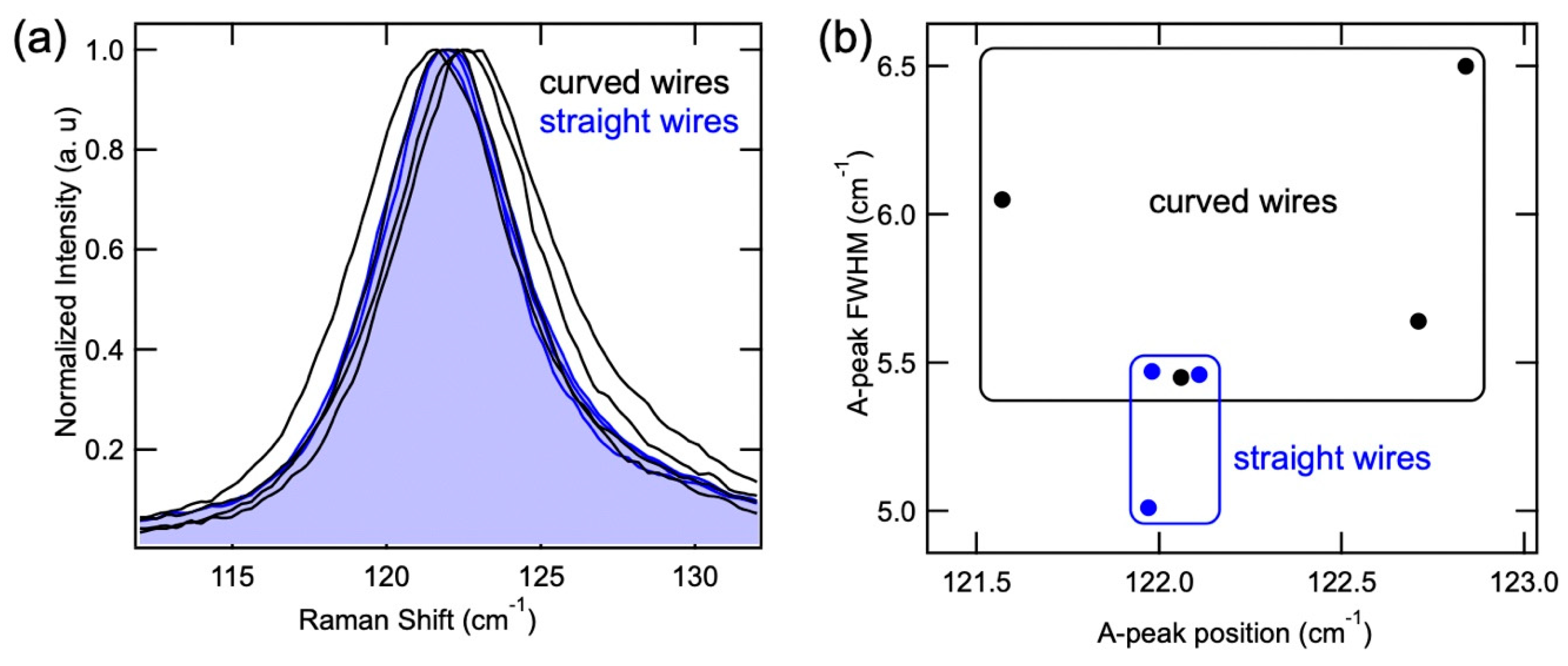
3.2. Characterizations of Te Nanowires
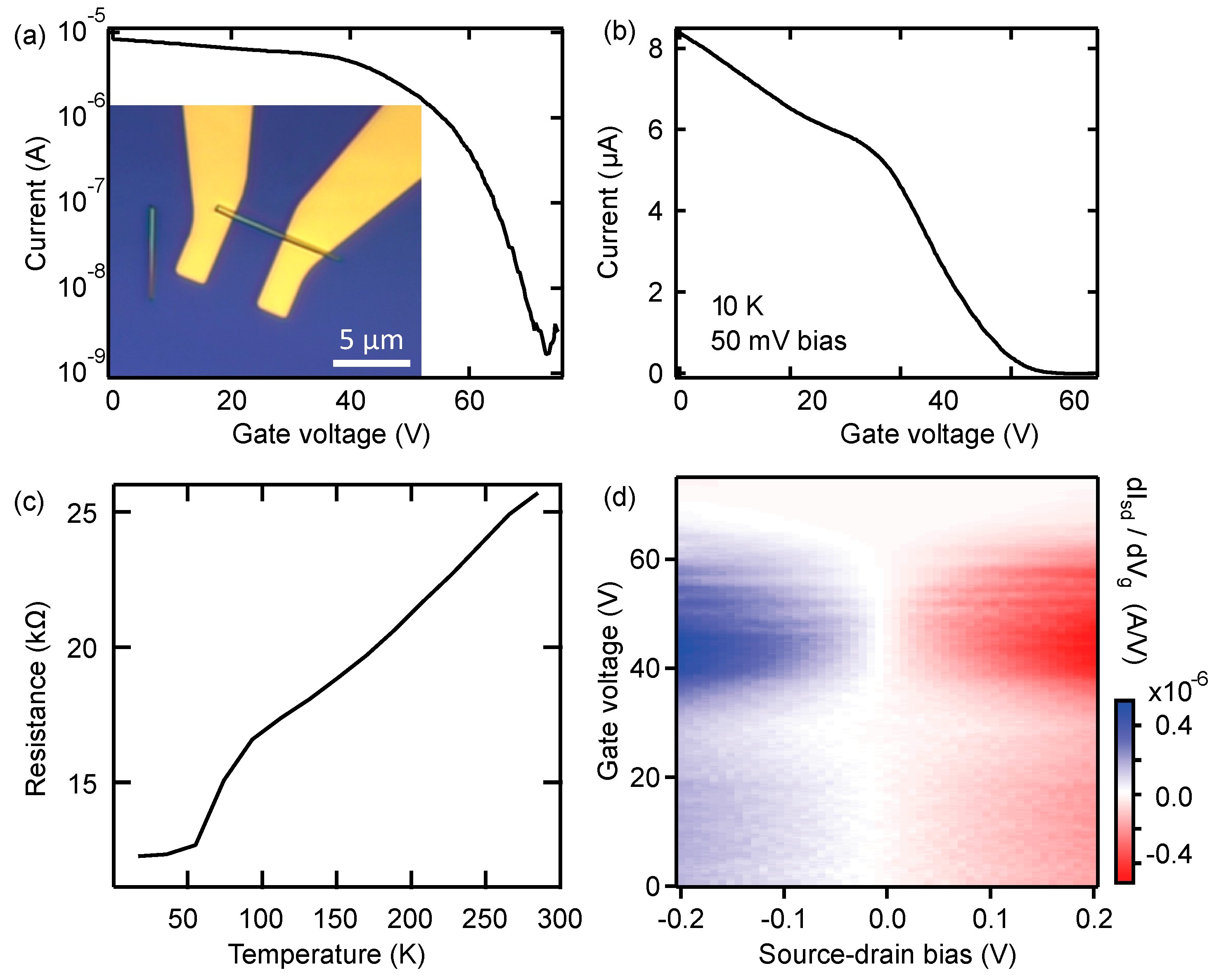
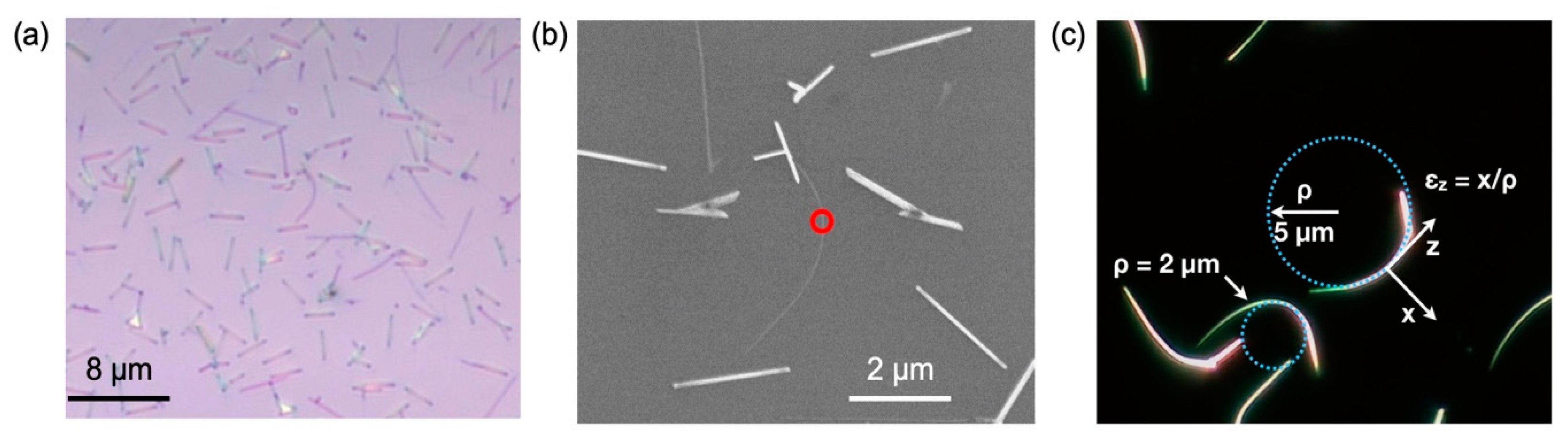
3.3. Strain Engineering of Te Nanowires
4. Discussion: Experimental Examination of the Weyl State in Strained Te Nanowires
Author Contributions
Funding
Conflicts of Interest
References
- Barron, L.D. Chirality and Life. Space Sci Rev 2008, 135, 187. [Google Scholar] [CrossRef]
- Wagniere, G.H. On Chirality and the Universal Asymmetry; Wiley-VCH: New York, NY, USA, 2007. [Google Scholar] [CrossRef]
- Bogdanov, A.; Hubert, A. Thermodynamically stable magnetic vortex states in magnetic crystals. J. Magn. Magn. Mater. 1994, 138, 255–269. [Google Scholar] [CrossRef]
- Chang, G.; Wieder, B.J.; Schindler, F.; Sanchez, D.S.; Belopolski, I.; Huang, S.-M.; Singh, B.; Wu, D.; Chang, T.-R.; Neupert, T.; et al. Topological quantum properties of chiral crystals. Nat. Mater. 2018, 17, 978–985. [Google Scholar] [CrossRef] [PubMed]
- Rikken, G.L.J.A.; Fölling, J.; Wyder, P. Electrical Magnetochiral Anisotropy. Phys. Rev. Lett. 2001, 87, 236602. [Google Scholar] [CrossRef] [PubMed]
- Sanchez, D.S.; Belopolski, I.; Cochran, T.A.; Xu, X.; Yin, J.-X.; Chang, G.; Xie, W.; Manna, K.; Süß, V.; Huang, C.-Y. Topological chiral crystals with helicoid-arc quantum states. Nature 2019, 567, 500. [Google Scholar] [CrossRef] [PubMed]
- Armitage, N.P.; Mele, E.J.; Vishwanath, A. Weyl and Dirac semimetals in three-dimensional solids. Rev. Mod. Phys. 2018, 90, 015001. [Google Scholar] [CrossRef]
- Hirayama, M.; Okugawa, R.; Ishibashi, S.; Murakami, S.; Miyake, T. Weyl Node and Spin Texture in Trigonal Tellurium and Selenium. Phys. Rev. Lett. 2015, 114, 206401. [Google Scholar] [CrossRef] [PubMed]
- Agapito, L.A.; Kioussis, N.; Goddard, W.A.; Ong, N.P. Novel Family of Chiral-Based Topological Insulators: Elemental Tellurium under Strain. Phys. Rev. Lett. 2013, 110, 176401. [Google Scholar] [CrossRef] [PubMed]
- Murakami, S.; Hirayama, M.; Okugawa, R.; Miyake, T. Emergence of topological semimetals in gap closing in semiconductors without inversion symmetry. Sci. Adv. 2017, 3, e1602680. [Google Scholar] [CrossRef]
- Huang, S.-M.; Xu, S.-Y.; Belopolski, I.; Lee, C.-C.; Chang, G.; Wang, B.; Alidoust, N.; Bian, G.; Neupane, M.; Zhang, C.; et al. A Weyl Fermion semimetal with surface Fermi arcs in the transition metal monopnictide TaAs class. Nat. Commun. 2015, 6, 7373. [Google Scholar] [CrossRef]
- Weng, H.; Fang, C.; Fang, Z.; Bernevig, B.A.; Dai, X. Weyl Semimetal Phase in Noncentrosymmetric Transition-Metal Monophosphides. Phys. Rev. X 2015, 5, 011029. [Google Scholar] [CrossRef]
- Lv, B.Q.; Weng, H.M.; Fu, B.B.; Wang, X.P.; Miao, H.; Ma, J.; Richard, P.; Huang, X.C.; Zhao, L.X.; Chen, G.F.; et al. Experimental Discovery of Weyl Semimetal TaAs. Phys. Rev. X 2015, 5, 031013. [Google Scholar] [CrossRef]
- Yang, L.X.; Liu, Z.K.; Sun, Y.; Peng, H.; Yang, H.F.; Zhang, T.; Zhou, B.; Zhang, Y.; Guo, Y.F.; Rahn, M.; et al. Weyl semimetal phase in the non-centrosymmetric compound TaAs. Nat. Phys. 2015, 11, 728–732. [Google Scholar] [CrossRef]
- Xu, S.-Y.; Alidoust, N.; Belopolski, I.; Yuan, Z.; Bian, G.; Chang, T.-R.; Zheng, H.; Strocov, V.N.; Sanchez, D.S.; Chang, G.; et al. Discovery of a Weyl fermion state with Fermi arcs in niobium arsenide. Nat. Phys. 2015, 11, 748–754. [Google Scholar] [CrossRef]
- Souma, S.; Wang, Z.; Kotaka, H.; Sato, T.; Nakayama, K.; Tanaka, Y.; Kimizuka, H.; Takahashi, T.; Yamauchi, K.; Oguchi, T.; et al. Direct observation of nonequivalent Fermi-arc states of opposite surfaces in the noncentrosymmetric Weyl semimetal NbP. Phys. Rev. B 2016, 93, 161112. [Google Scholar] [CrossRef]
- Xu, D.-F.; Du, Y.-P.; Wang, Z.; Li, Y.-P.; Niu, X.-H.; Yao, Q.; Dudin, P.; Xu, Z.-A.; Wan, X.-G.; Feng, D.-L. Observation of Fermi Arcs in Non-Centrosymmetric Weyl Semi-Metal Candidate NbP. Chin. Phys. Lett. 2015, 32, 107101. [Google Scholar] [CrossRef]
- Liu, Z.K.; Yang, L.X.; Sun, Y.; Zhang, T.; Peng, H.; Yang, H.F.; Chen, C.; Zhang, Y.; Guo, Y.F.; Prabhakaran, D.; et al. Evolution of the Fermi surface of Weyl semimetals in the transition metal pnictide family. Nat. Mater. 2015, 15, 27. [Google Scholar] [CrossRef]
- Xu, N.; Weng, H.M.; Lv, B.Q.; Matt, C.E.; Park, J.; Bisti, F.; Strocov, V.N.; Gawryluk, D.; Pomjakushina, E.; Conder, K.; et al. Observation of Weyl nodes and Fermi arcs in tantalum phosphide. Nat. Commun. 2015, 7, 11006. [Google Scholar] [CrossRef]
- Xu, S.-Y.; Belopolski, I.; Sanchez, D.S.; Zhang, C.; Chang, G.; Guo, C.; Bian, G.; Yuan, Z.; Lu, H.; Chang, T.-R.; et al. Experimental discovery of a topological Weyl semimetal state in TaP. Sci. Adv. 2015, 1. [Google Scholar] [CrossRef]
- Xu, S.-Y.; Belopolski, I.; Alidoust, N.; Neupane, M.; Bian, G.; Zhang, C.; Sankar, R.; Chang, G.; Yuan, Z.; Lee, C.-C.; et al. Discovery of a Weyl Fermion semimetal and topological Fermi arcs. Science 2015, 349, 613–617. [Google Scholar] [CrossRef]
- Nakayama, K.; Kuno, M.; Yamauchi, K.; Souma, S.; Sugawara, K.; Oguchi, T.; Sato, T.; Takahashi, T. Band splitting and Weyl nodes in trigonal tellurium studied by angle-resolved photoemission spectroscopy and density functional theory. Phys. Rev. B 2017, 95, 125204. [Google Scholar] [CrossRef]
- Qiu, G.; Niu, C.; Wang, Y.; Si, M.; Zhang, Z.; Wu, W.; Ye, P.D. Quantum Hall Effect of Massive Weyl Fermions in n-type Tellurene Films. arXiv 2019, arXiv:1908.11495. [Google Scholar]
- Keller, R.; Holzapfel, W.B.; Schulz, H. Effect of pressure on the atom positions in Se and Te. Phys. Rev. B 1977, 16, 4404–4412. [Google Scholar] [CrossRef]
- Cheon, G.; Duerloo, K.-A.N.; Sendek, A.D.; Porter, C.; Chen, Y.; Reed, E.J. Data Mining for New Two- and One-Dimensional Weakly Bonded Solids and Lattice-Commensurate Heterostructures. Nano Lett. 2017, 17, 1915–1923. [Google Scholar] [CrossRef] [PubMed]
- Zhang, B.; Dai, W.; Ye, X.; Zuo, F.; Xie, Y. Photothermally Assisted Solution-Phase Synthesis of Microscale Tubes, Rods, Shuttles, and an Urchin-Like Assembly of Single-Crystalline Trigonal Selenium. Angew. Chem. Int. Ed. 2006, 45, 2571–2574. [Google Scholar] [CrossRef]
- Liang, F.; Qian, H. Synthesis of tellurium nanowires and their transport property. Mater. Chem. Phys. 2009, 113, 523–526. [Google Scholar] [CrossRef]
- Lan, W.-J.; Yu, S.-H.; Qian, H.-S.; Wan, Y. Dispersibility, Stabilization, and Chemical Stability of Ultrathin Tellurium Nanowires in Acetone: Morphology Change, Crystallization, and Transformation into TeO2 in Different Solvents. Langmuir 2007, 23, 3409–3417. [Google Scholar] [CrossRef] [PubMed]
- Zhang, S.-Y.; Liu, Y.; Ma, X.; Chen, H.-Y. Rapid, Large-Scale Synthesis and Electrochemical Behavior of Faceted Single-Crystalline Selenium Nanotubes. J. Phys. Chem. B 2006, 110, 9041–9047. [Google Scholar] [CrossRef]
- Ren, L.; Zhang, H.; Tan, P.; Chen, Y.; Zhang, Z.; Chang, Y.; Xu, J.; Yang, F.; Yu, D. Hexagonal Selenium Nanowires Synthesized via Vapor-Phase Growth. J. Phys. Chem. B 2004, 108, 4627–4630. [Google Scholar] [CrossRef]
- Yang, Y.; Wang, K.; Liang, H.-W.; Liu, G.-Q.; Feng, M.; Xu, L.; Liu, J.-W.; Wang, J.-L.; Yu, S.-H. A new generation of alloyed/multimetal chalcogenide nanowires by chemical transformation. Sci. Adv. 2015, 1, e1500714. [Google Scholar] [CrossRef]
- Gates, B.; Mayers, B.; Cattle, B.; Xia, Y. Synthesis and Characterization of Uniform Nanowires of Trigonal Selenium. Adv. Funct. Mater. 2002, 12, 219–227. [Google Scholar] [CrossRef]
- Gautam, U.K.; Rao, C.N.R. Controlled synthesis of crystalline tellurium nanorods, nanowires, nanobelts and related structures by a self-seeding solution process. J. Mater. Chem. 2004, 14, 2530–2535. [Google Scholar] [CrossRef]
- Lu, Q.; Gao, F.; Komarneni, S. Cellulose-Directed Growth of Selenium Nanobelts in Solution. Chem. Mater. 2006, 18, 159–163. [Google Scholar] [CrossRef]
- Du, Y.; Qiu, G.; Wang, Y.; Si, M.; Xu, X.; Wu, W.; Ye, P.D. One-Dimensional van der Waals Material Tellurium: Raman Spectroscopy under Strain and Magneto-Transport. Nano Lett. 2017, 17, 3965–3973. [Google Scholar] [CrossRef] [PubMed]
- Huang, X.; Guan, J.; Lin, Z.; Liu, B.; Xing, S.; Wang, W.; Guo, J. Epitaxial Growth and Band Structure of Te Film on Graphene. Nano Lett. 2017, 17, 4619–4623. [Google Scholar] [CrossRef] [PubMed]
- Zhu, Z.; Cai, X.; Yi, S.; Chen, J.; Dai, Y.; Niu, C.; Guo, Z.; Xie, M.; Liu, F.; Cho, J.-H.; et al. Multivalency-Driven Formation of Te-Based Monolayer Materials: A Combined First-Principles and Experimental study. Phys. Rev. Lett. 2017, 119, 106101. [Google Scholar] [CrossRef] [PubMed]
- Wang, Y.; Qiu, G.; Wang, R.; Huang, S.; Wang, Q.; Liu, Y.; Du, Y.; Goddard, W.A.; Kim, M.J.; Xu, X.; et al. Field-effect transistors made from solution-grown two-dimensional tellurene. Nat. Electron. 2018, 1, 228–236. [Google Scholar] [CrossRef]
- Churchill, H.O.H.; Salamo, G.J.; Yu, S.-Q.; Hironaka, T.; Hu, X.; Stacy, J.; Shih, I. Toward Single Atom Chains with Exfoliated Tellurium. Nanoscale Res. Lett. 2017, 12, 488. [Google Scholar] [CrossRef]
- Mohanty, P.; Kang, T.; Kim, B.; Park, J. Synthesis of Single Crystalline Tellurium Nanotubes with Triangular and Hexagonal Cross Sections. J. Phys. Chem. B 2006, 110, 791–795. [Google Scholar] [CrossRef]
- Hawley, C.J.; Beatty, B.R.; Chen, G.; Spanier, J.E. Shape-Controlled Vapor-Transport Growth of Tellurium Nanowires. Cryst. Growth Des. 2012, 12, 2789–2793. [Google Scholar] [CrossRef]
- Tao, H.; Liu, H.M.; Qin, D.H.; Chan, K.; Chen, J.W.; Cao, Y. High Mobility Field Effect Transistor from Solution-Processed Needle-Like Tellurium Nanowires. J. Nanosci. Nanotechnol. 2010, 10, 7997–8003. [Google Scholar] [CrossRef] [PubMed]
- Zhou, G.Y.; Addou, R.; Wang, Q.X.; Honari, S.; Cormier, C.R.; Cheng, L.X.; Yue, R.Y.; Smyth, C.M.; Laturia, A.; Kim, J.; et al. High-Mobility Helical Tellurium Field-Effect Transistors Enabled by Transfer-Free, Low-Temperature Direct Growth. Adv. Mater. 2018, 30, 1803109. [Google Scholar] [CrossRef] [PubMed]
- Dayeh, S.A.; Aplin, D.P.R.; Zhou, X.T.; Yu, P.K.L.; Yu, E.T.; Wang, D.L. High electron mobility InAs nanowire field-effect transistors. Small 2007, 3, 326–332. [Google Scholar] [CrossRef]
- Li, P.; Appelbaum, I. Intrinsic two-dimensional states on the pristine surface of tellurium. Phys. Rev. B 2018, 97, 201402. [Google Scholar] [CrossRef]
- Yu, T.; Ni, Z.; Du, C.; You, Y.; Wang, Y.; Shen, Z. Raman Mapping Investigation of Graphene on Transparent Flexible Substrate: The Strain Effect. J. Phys. Chem. C 2008, 112, 12602–12605. [Google Scholar] [CrossRef]
- Wu, W.; Wang, L.; Yu, R.; Liu, Y.; Wei, S.-H.; Hone, J.; Wang, Z.L. Piezophototronic Effect in Single-Atomic-Layer MoS2 for Strain-Gated Flexible Optoelectronics. Adv. Mater. 2016, 28, 8463–8468. [Google Scholar] [CrossRef] [PubMed]
- Lee, J.; Ha, T.; Parrish, K.N.; Chowdhury, S.F.; Tao, L.; Dodabalapur, A.; Akinwande, D. High-Performance Current Saturating Graphene Field-Effect Transistor with Hexagonal Boron Nitride Dielectric on Flexible Polymeric Substrates. IEEE Electron Device Lett. 2013, 34, 172–174. [Google Scholar] [CrossRef]
- Tweedie, M.E.P.; Sheng, Y.; Sarwat, S.G.; Xu, W.; Bhaskaran, H.; Warner, J.H. Inhomogeneous Strain Release during Bending of WS2 on Flexible Substrates. Acs Appl. Mater. Interfaces 2018, 10, 39177–39186. [Google Scholar] [CrossRef]
- Torrie, B.H. Raman spectrum of tellurium. Solid State Commun. 1970, 8, 1899–1901. [Google Scholar] [CrossRef]
- Pine, A.S.; Dresselhaus, G. Raman Spectra and Lattice Dynamics of Tellurium. Phys. Rev. B 1971, 4, 356–371. [Google Scholar] [CrossRef]
- Marini, C.; Cherisi, D.; Lavagnini, M.; di Castro, D.; Petrillo, C.; Degiorgi, L.; Scandolo, S.; Postorino, P. High-pressure phases of crystalline tellurium: A combined Raman and ab initio study. Phys. Rev. B. 2012, 86, 064103. [Google Scholar] [CrossRef]
- Hu, J.; Xu, S.-Y.; Ni, N.; Mao, Z. Transport of Topological Semimetals. Annu. Rev. Mater. Res. 2019, 49, 207–252. [Google Scholar] [CrossRef]
- Bernevig, A.; Weng, H.; Fang, Z.; Dai, X. Recent Progress in the Study of Topological Semimetals. J. Phys. Soc. Jpn. 2018, 87, 041001. [Google Scholar] [CrossRef]
- Kumar, N.; Guin, S.N.; Felser, C.; Shekhar, C. Planar Hall effect in the Weyl semimetal GdPtBi. Phys. Rev. B 2018, 98, 041103. [Google Scholar] [CrossRef]
- Burkov, A.A. Giant planar Hall effect in topological metals. Phys. Rev. B 2017, 96, 041110. [Google Scholar] [CrossRef]
- Nandy, S.; Sharma, G.; Taraphder, A.; Tewari, S. Chiral Anomaly as the Origin of the Planar Hall Effect in Weyl Semimetals. Phys. Rev. Lett. 2017, 119, 176804. [Google Scholar] [CrossRef] [PubMed]
- Li, H.; Wang, H.-W.; He, H.; Wang, J.; Shen, S.-Q. Giant anisotropic magnetoresistance and planar Hall effect in the Dirac semimetal Cd3As2. Phys. Rev. B 2018, 97, 201110. [Google Scholar] [CrossRef]
- Li, C.-Z.; Wang, L.-X.; Liu, H.; Wang, J.; Liao, Z.-M.; Yu, D.-P. Giant negative magnetoresistance induced by the chiral anomaly in individual Cd3As2 nanowires. Nat. Commun. 2015, 6, 10137. [Google Scholar] [CrossRef]
- Assaf, B.A.; Phuphachong, T.; Kampert, E.; Volobuev, V.V.; Mandal, P.S.; Sánchez-Barriga, J.; Rader, O.; Bauer, G.; Springholz, G.; de Vaulchier, L.A.; et al. Negative Longitudinal Magnetoresistance from the Anomalous N=0 Landau Level in Topological Materials. Phys. Rev. Lett. 2017, 119, 106602. [Google Scholar] [CrossRef]
- Silbermann, R.; Landwehr, G. Surface quantum oscillations in accumulation and inversion layers on tellurium. Solid State Commun. 1975, 16, 1055–1058. [Google Scholar] [CrossRef]
- Von Klitzing, K.; Landwehr, G. Surface quantum states in tellurium. Solid State Commun. 1971, 9, 2201–2205. [Google Scholar] [CrossRef]
- Qiu, G.; Wang, Y.; Nie, Y.; Zheng, Y.; Cho, K.; Wu, W.; Ye, P.D. Quantum Transport and Band Structure Evolution under High Magnetic Field in Few-Layer Tellurene. Nano Lett. 2018, 18, 5760–5767. [Google Scholar] [CrossRef] [PubMed]
- Liang, T.; Lin, J.; Gibson, Q.; Kushwaha, S.; Liu, M.; Wang, W.; Xiong, H.; Sobota, J.A.; Hashimoto, M.; Kirchmann, P.S.; et al. Anomalous Hall effect in ZrTe5. Nat. Phys. 2018, 14, 451–455. [Google Scholar] [CrossRef]
- Wang, Y.J.; Gong, J.X.; Liang, D.D.; Ge, M.; Wang, J.R.; Zhu, W.K.; Zhang, C.J. Planar Hall effect in type-II Weyl semimetal WTe2. arXiv 2018, arXiv:1801.05929. [Google Scholar]
- Reis, R.D.D.; Ajeesh, M.O.; Kumar, N.; Arnold, F.; Shekhar, C.; Naumann, M.; Schmidt, M.; Nicklas, M.; Hassinger, E. On the search for the chiral anomaly in Weyl semimetals: The negative longitudinal magnetoresistance. New J. Phys. 2016, 18, 085006. [Google Scholar] [CrossRef]
- Liang, S.; Lin, J.; Kushwaha, S.; Xing, J.; Ni, N.; Cava, R.J.; Ong, N.P. Experimental tests of the chiral anomaly magnetoresistance in the Dirac-Weyl semimetals Na3Bi and GdPtBi. Phys. Rev. X 2018, 8, 031002. [Google Scholar] [CrossRef]
- Fete, A.; Rossi, L.; Augieri, A.; Senatore, C. Ionic liquid gating of ultra-thin YBa2Cu3O7-x films. Appl. Phys. Lett. 2016, 109, 4. [Google Scholar] [CrossRef]
- Hellerstedt, J.; Yudhistira, I.; Edmonds, M.T.; Liu, C.; Collins, J.; Adam, S.; Fuhrer, M.S. Electrostatic modulation of the electronic properties of Dirac semimetal Na3Bi thin films. Phys. Rev. Mater. 2017, 1, 5. [Google Scholar] [CrossRef]
- Nishihaya, S.; Uchida, M.; Nakazawa, Y.; Kriener, M.; Kozuka, Y.; Taguchi, Y.; Kawasaki, M. Gate-tuned quantum Hall states in Dirac semimetal (Cd1-xZnx)3As2. Sci. Adv. 2018, 4, 8. [Google Scholar] [CrossRef]


© 2019 by the authors. Licensee MDPI, Basel, Switzerland. This article is an open access article distributed under the terms and conditions of the Creative Commons Attribution (CC BY) license (http://creativecommons.org/licenses/by/4.0/).
Share and Cite
Basnet, R.; Doha, M.H.; Hironaka, T.; Pandey, K.; Davari, S.; Welch, K.M.; Churchill, H.O.H.; Hu, J. Growth and Strain Engineering of Trigonal Te for Topological Quantum Phases in Non-Symmorphic Chiral Crystals. Crystals 2019, 9, 486. https://doi.org/10.3390/cryst9100486
Basnet R, Doha MH, Hironaka T, Pandey K, Davari S, Welch KM, Churchill HOH, Hu J. Growth and Strain Engineering of Trigonal Te for Topological Quantum Phases in Non-Symmorphic Chiral Crystals. Crystals. 2019; 9(10):486. https://doi.org/10.3390/cryst9100486
Chicago/Turabian StyleBasnet, Rabindra, M. Hasan Doha, Takayuki Hironaka, Krishna Pandey, Shiva Davari, Katie M. Welch, Hugh O. H. Churchill, and Jin Hu. 2019. "Growth and Strain Engineering of Trigonal Te for Topological Quantum Phases in Non-Symmorphic Chiral Crystals" Crystals 9, no. 10: 486. https://doi.org/10.3390/cryst9100486
APA StyleBasnet, R., Doha, M. H., Hironaka, T., Pandey, K., Davari, S., Welch, K. M., Churchill, H. O. H., & Hu, J. (2019). Growth and Strain Engineering of Trigonal Te for Topological Quantum Phases in Non-Symmorphic Chiral Crystals. Crystals, 9(10), 486. https://doi.org/10.3390/cryst9100486