
Article

Influence of Humidity on the Domain-Structure Evolution During Local Switching in a (100) Cut Bi4Ti3O12 Single Crystal

School of Natural Sciences and Mathematics, Ural Federal University, Ekaterinburg 620002, Russia
*
Author to whom correspondence should be addressed.
Crystals 2026, 16(5), 315; https://doi.org/10.3390/cryst16050315
Submission received: 9 April 2026 / Revised: 2 May 2026 / Accepted: 6 May 2026 / Published: 8 May 2026
(This article belongs to the Special Issue Advanced Research on Ferroelectric Materials)

Abstract

The formation and growth of isolated domains during local switching by a biased tip of a scanning probe microscope in a (100) cut of a bismuth titanate Bi4Ti3O12 single crystal were studied experimentally. The as-grown domain structure consists of two domain types: a-type (out-of-plane) and b-type (in-plane). Local switching of the a-type domain area leads to anisotropic growth of a hexagonal a-type domain (a-a switching) with 180° walls. The dependence of the domain size on the pulse duration during domain growth along the b-axis was considered in terms of the anisotropic current-limited domain wall motion. Local switching of the b-type domain area leads to formation of a hexagonal a-type domain (b-a switching) with 90° walls increasing in size linearly with the applied voltage. The dependence of the domain size on the pulse duration was measured over a wide range of humidities. The increase in the domain size at moderate humidity is attributed to the effect of the water meniscus. The decrease in the domain size at high humidity is attributed to backswitching under the action of the residual depolarization field, facilitated by a conductive water layer on the side surfaces of the sample. The obtained results provide useful insights into the domain kinetics of ferroelectrics with C2 symmetry and can pave the way for the development of domain engineering techniques. The obtained results establish a direct relationship between local switching kinetics, crystallographic anisotropy, and environmental conditions. This provides the scientific community with a new framework for understanding domain wall motion in multiaxial ferroelectrics, which is essential for the development of stable and reliable domain-engineered devices.

1. Introduction

Ferroelectric materials are widely used to create various nonlinear optical [1] and data storage devices [2,3] or microelectromechanical systems [4]. High-temperature piezoelectric materials capable of operating at temperatures up to 670 °C are important for practical applications [5,6]. It has been reported that bismuth-containing ferroelectrics with a layered structure (Aurivillius phase) have a high TC (above 500 °C), high temperature stability of functional properties, and a low aging rate, which makes them promising for high-temperature applications [7,8]. It should also be mentioned that TiO2-based systems possess catalytic and piezocatalytic properties, which are promising for the degradation of organic pollutants, disinfection, electrochemical polymerization, and water splitting [9,10,11].
Materials of the Aurivillius phase family [12,13] have the general formula [Me2O2]2+[Am−1BmO3m+1]2− and consist of [Me2O2]2+ layers with a fluorite structure and m [Am−1BmO3m+1]2− layers with a perovskite structure [14], alternating along the pseudotetragonal c-axis. One of the representatives of this family is layered bismuth titanate Bi4Ti3O12, BiT (Me, A = Bi, B = Ti, m = 3, [Bi2O2]2+[Bi2Ti3O10]2−). BiT has a relatively high value of ferroelectric phase-transition temperature (TC = 675 °C) and spontaneous polarization (Ps = 50 μC/cm2). The pronounced spontaneous recovery of the initial domain state was observed in BiT after applying short reading-field pulses (so-called backswitching or the t*-effect), suggesting its application in data storage [15]. Layered bismuth perovskite SrBi2Nb2O9 is widely used in Ferroelectric Random Access Memory (FeRAM) [16,17]. Recently, memristors based on BiT thin films have been proposed as promising components for neuromorphic computing devices [18,19].
In the ferroelectric phase, BiT belongs to the monoclinic symmetry C2 (a = 5.4432 (5) Å, b = 5.4099 (5) Å, c = 32.821 (2) Å) with a monoclinic angle β = 89.977° [20], which is extremely close to 90°, so this structure is frequently approximated as orthorhombic [21]. It has two independently switchable polarization components, Ps(a) and Ps(c), in the ac plane of the unit cell, which leads to the formation of a complex domain structure [22]. BiT is a multiaxial ferroelectric with eight possible polarization directions and five types of domain walls: 9°, 90°, 91°, 171°, and 180° [22,23,24]. The most typical domain structure in BiT consists of stripe domains with 90° walls [23,25], similar to such multiaxial ferroelectrics as barium titanate (BaTiO3) and lead-zirconate titanate (Pb0.5Zr0.5TiO3) [26,27]. The domain structure in BiT crystals has been imaged by various methods: optical microscopy [28], confocal Raman microscopy [29,30], scanning electron microscopy [31], dark-field transmission electron microscopy [32], and piezoresponse force microscopy (PFM) [33,34,35].
Polarization reversal processes with kinetics of 90° domain walls under the influence of a low-frequency electric field were investigated on the ab-plane in a BiT crystal [36,37]. The polar axis lies at an angle of 4.5° to the cleavage plane [5]. The presence of a perfect cleavage plane allowed us to visualize the domain structure on the (001) surface or c-cut of BiT samples prepared without polishing. It should be noted that studying forward domain growth (in the polar direction) on the sample surface [38] can only be realized on a polished a-cut.
The striped domain structure is observed on the a-cut of BiT crystals [22], similar to ferroelectric crystals with C2 symmetry [39], such as triglycine sulphate (NH2CH2COOH)3·H2SO4 (TGS) [40], potassium titanyl-phosphate family KTiOPO4 [41], and gadolinium molybdate Gd2(MoO4)3 [42].
The scanning probe microscopy (SPM) is widely applied for investigation of various properties with high spatial resolution [43,44,45]. Local switching by a biased tip of a SPM is one of the most powerful methods to study domain kinetics at the nanoscale [46]. Relative humidity has been shown to have a significant influence on the size of the created domains [47,48]. The adsorbed water can create a meniscus at the SPM tip being in contact with the sample [49] and a high-resistivity layer covering the sample surface [50,51]. Recently, local switching by a conductive tip in a ferroelectric covered by a high-resistivity electrode has been considered in terms of “current limited switching” [52,53,54]. The Stefan approach has been applied to solve the problem of domain wall motion in ferroelectric thin films covered by linear high-resistivity stripe electrodes [52,53]. Domain growth at high humidity in KTiOPO4 crystal has been attributed to the influence of the surface absorbed water layer, which acts as a high-resistivity electrode, thus enabling external screening [54]. A current-limited wall motion regime driven by internal bulk screening has been demonstrated during local switching in polydomain TGS crystals [55]. Moreover, in BiT, it is reasonable to consider the influence of the above-mentioned pronounced backswitching process [56,57].
As far as we know, the kinetics of isolated domains during local switching and forward domain growth have not been studied in BiT. Here, we present the results of the experimental study of isolated domain growth created by a biased tip of a scanning probe microscope and visualized by PFM on a (100) cut of BiT single crystals. We studied the influence of relative humidity on domain growth during local switching.

2. Materials and Methods

The studied BiT single crystal samples were grown using the flux method [58]. The initial crystals, with a thickness of about 0.7 mm, were cut perpendicularly to the (100) direction (a-cut) into bars with a width of 0.5 mm using a DAD3220 automatic dicing saw (Disco Corp., Tokyo, Japan) with a Disco Z09-SD3000-Y1-90 55x0.1 A2X40-L diamond blade, at a rotation speed of 20,000 rpm and a feed rate of 0.5 mm/s. Then, the side surfaces (bc-plane) of the samples were carefully polished with diamond paste with a particle size decreasing from 6 to 0.25 µm. Final polishing was carried out with a mixture of colloidal silicon dioxide solution (SF1 Polishing Suspension, Logitech, London, UK). The sample thickness was after polishing about 0.4 mm, and the surface roughness Sa, estimated using SPM, was below 10 nm. The bottom surface was glued to a metal conductive substrate with silver paste.
A NTEGRA Aura scanning probe microscope (NT-MDT, Zelenograd, Russia) was used for the domain visualization and local switching. The imaging was performed using the built-in PFM mode with voltage modulation at an amplitude of 5–10 V and a frequency of 20 kHz far from contact resonance. Commercial NSC18 probes with a conductive Ti/Pt coating (MikroMasch, Sofia, Bulgaria) were used, with a curvature radius of 35 nm, resonance frequency of 70 kHz, and spring constant of 3.5 N/m. To represent domain structure images, the value of the mixed PFM signal (R·Cos (θ), where R and θ are the amplitude and phase of the piezoresponse signal), was used [59].
Rectangular switching pulses with an amplitude Usw from 50 to 300 V and duration tsw from 100 ms to 464 s were generated by a NI-6251 multifunctional Data Acquisition board (National Instruments, Austin, TX, USA) and a Trek-677B high-voltage amplifier (TREK, Inc., Lockport, NY, USA). Domain sizes were measured in three independent experiments, and the mean value was used for analysis. All experiments were carried out at a nitrogen flow rate of about 3 L/min and a controlled relative humidity (RH) ranging from 0 to 60%. RH was controlled by mixing dry and water-saturated nitrogen streams and monitored with a hygrometer placed inside the measurement chamber. After each humidity change, a stabilization time of 1 h was allowed before any switching experiments were performed. At the end of the switching pulse, before voltage switch-off, the tip was withdrawn from the surface to diminish the backswitching effect [56].

3. Results

3.1. As-Grown Domain Structure

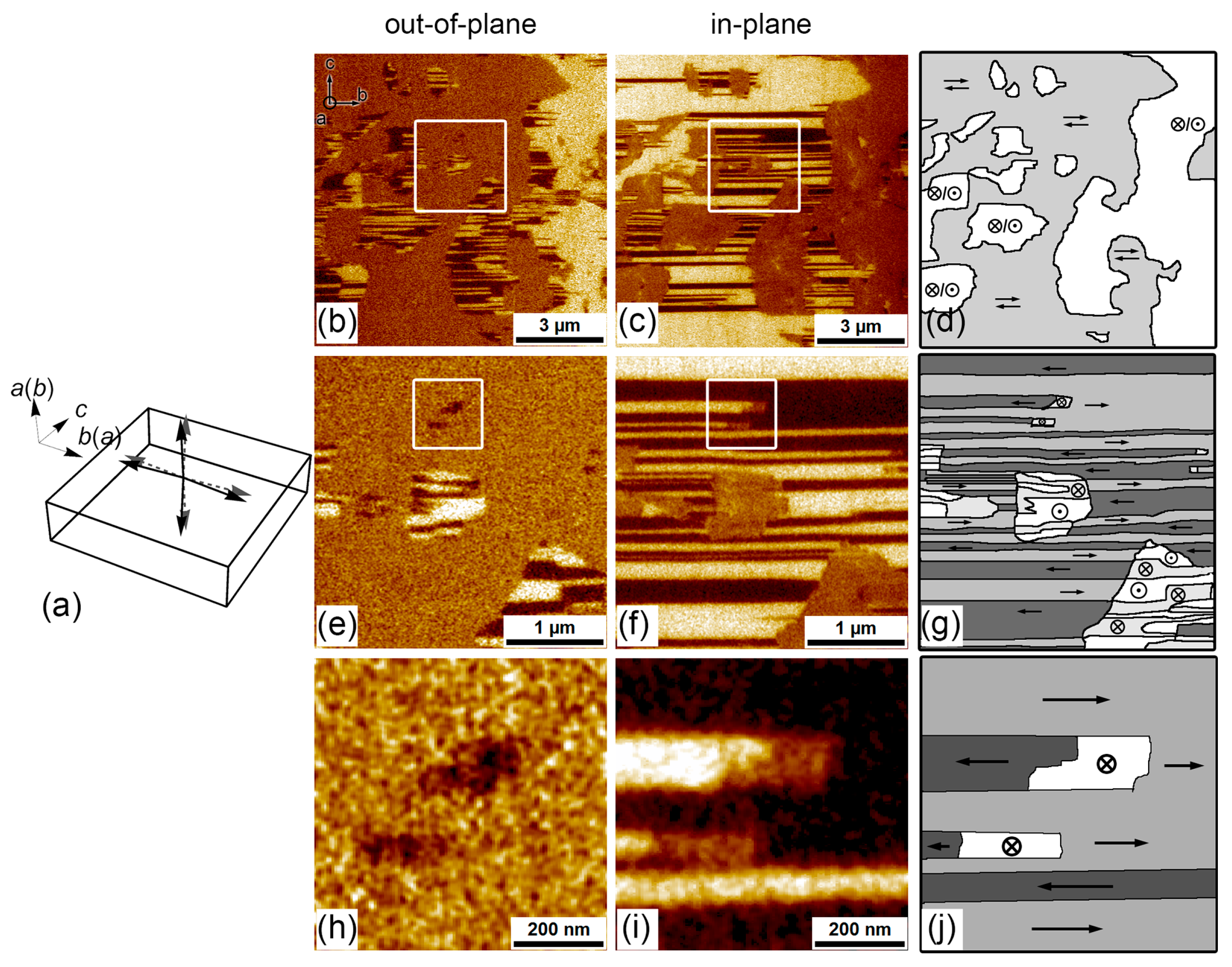
In the studied a-cut samples, two types of domains were distinguished. So-called b-type (in-plane) domains have four directions of spontaneous polarization on the sample surface, which deviate from the ab plane by 4.5°. So-called a-type (out-of-plane) domains have four directions of spontaneous polarization at the ac plane, which deviate from the a-axis by 4.5° (Figure 1a). The initial domain structure consists of irregularly shaped regions (Figure 1b–g) [32]. Each region is patterned by antiparallel stripe domains of the same type with a width of 50 to 500 nm (Figure 1e–g). It should be noted that in the b-type matrix, at the ends of the striped b-type domains, there are small a-type domains with 90° walls (Figure 1h–j).
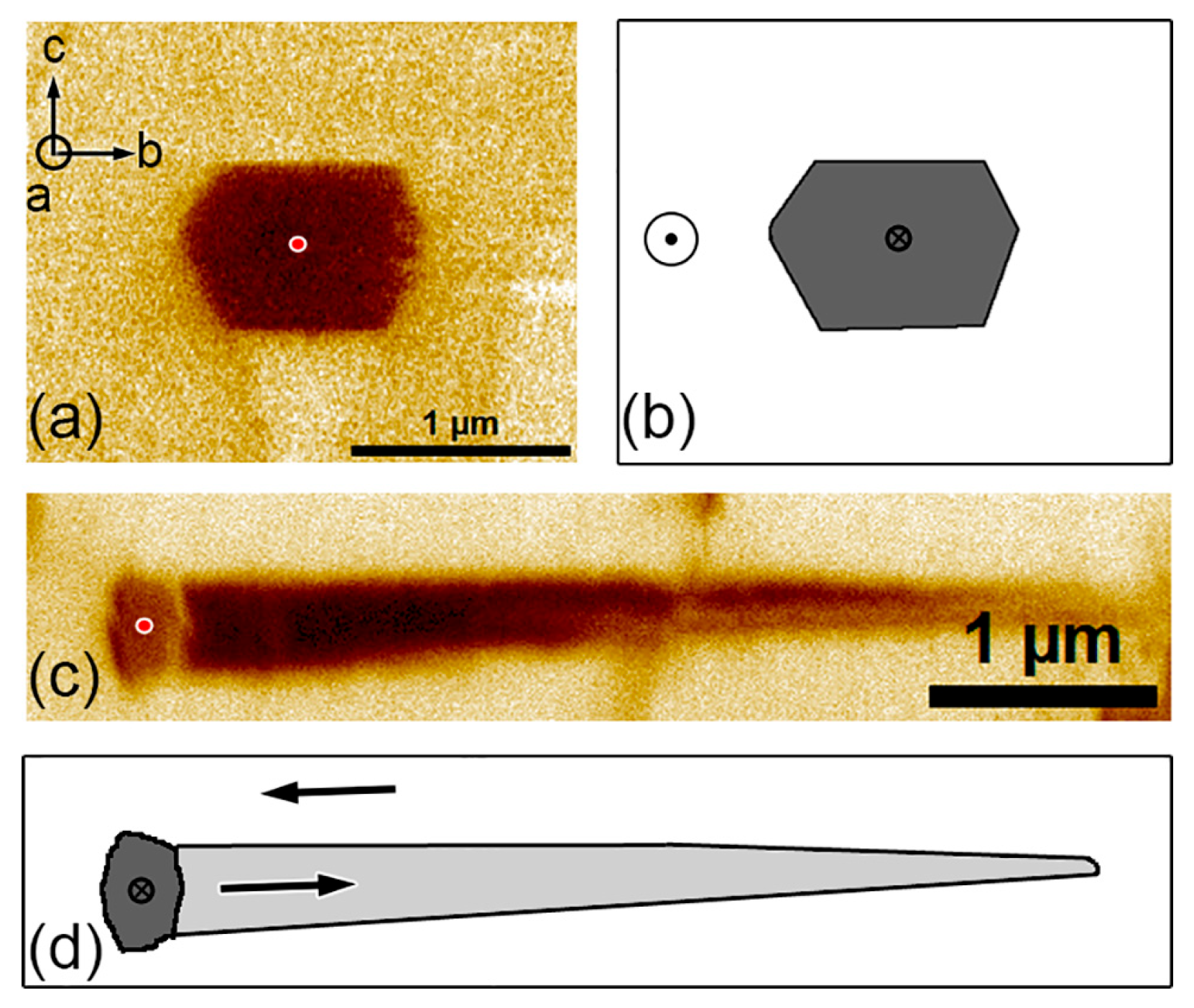
The formation of isolated domains as a result of local switching was investigated in large domains of a- and b-types. Local switching of an a-type domain leads to formation of a hexagonal a-type domain (a-a switching) with 180° walls (Figure 2a,b). The created domains remained stable for more than 48 h (See Supplementary). The formation of hexagonal domains by local switching in a ferroelectric with C2 symmetry was observed in KTP crystals [54].

3.2. Local Switching

Local switching of the b-type domain leads to the formation of an a-type domain (b-a switching) with 90° walls (Figure 2c,d). Moreover, a wedge-shaped b-type domain with 180° domain walls and a length of up to several microns is formed (Figure 2c,d) [38]. Similar wedge-shaped domains are formed during local switching on non-polar cuts of uniaxial ferroelectric crystals [38]. Previously, multi-step domain growth with the formation of domains of different types was observed during local switching in Cu-doped sodium-potassium niobate crystals (K0.5Na0.5)NbO3 [60,61].
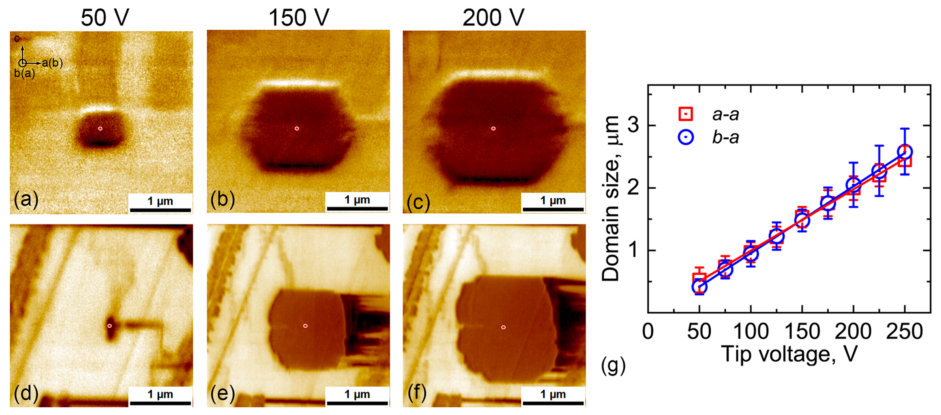
To study the dependence of the domain shape on the amplitude and duration of the switching pulse, “step-by-step” local switching was carried out. A sequence of switching pulses with increasing amplitude and constant duration was applied, the resulting domains being visualized after each pulse (Figure 3a–c).
As a result of local switching in both a-a and b-a switching, a domain with out-of-plane polarization appeared (Figure 3a–f). The walls of the resulting domains are oriented perpendicular to the c direction (Figure 3c,f). At a pulse duration of 1 s and an RH of 30%, the minimal domain appeared at Usw = 50 V with a size along the c-axis of about 0.5 μm. These sizes increase linearly with increasing applied voltage (Figure 3g).
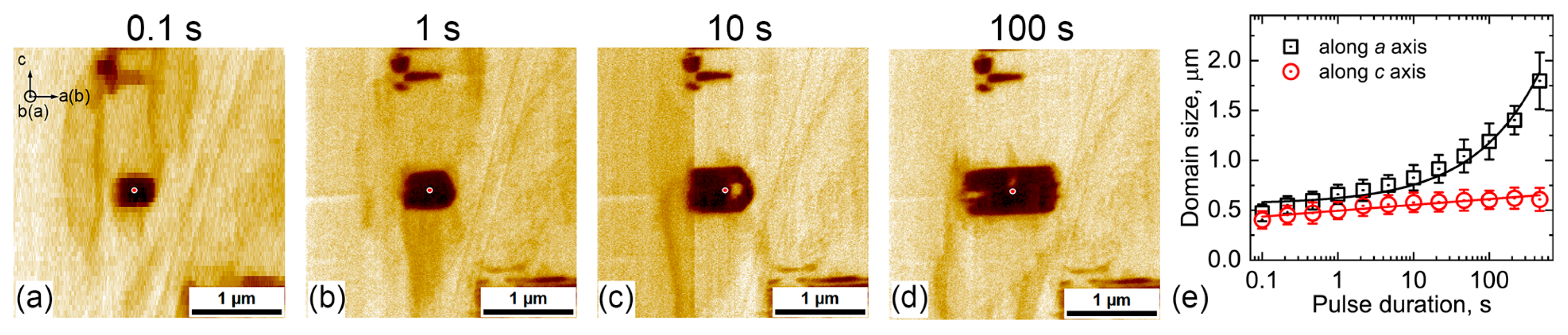
In the case of a-a switching, strong growth anisotropy was observed with increasing pulse duration (Figure 4). The domain size along the c-axis increases slowly, whereas the domain size along the a-axis increases significantly (Figure 4e). The domain growth anisotropy can be attributed to the known anisotropy of bulk conductivity [62,63]. Similar effects were observed previously during local switching in polydomain TGS crystals [55].

3.3. Influence of the Relative Humidity

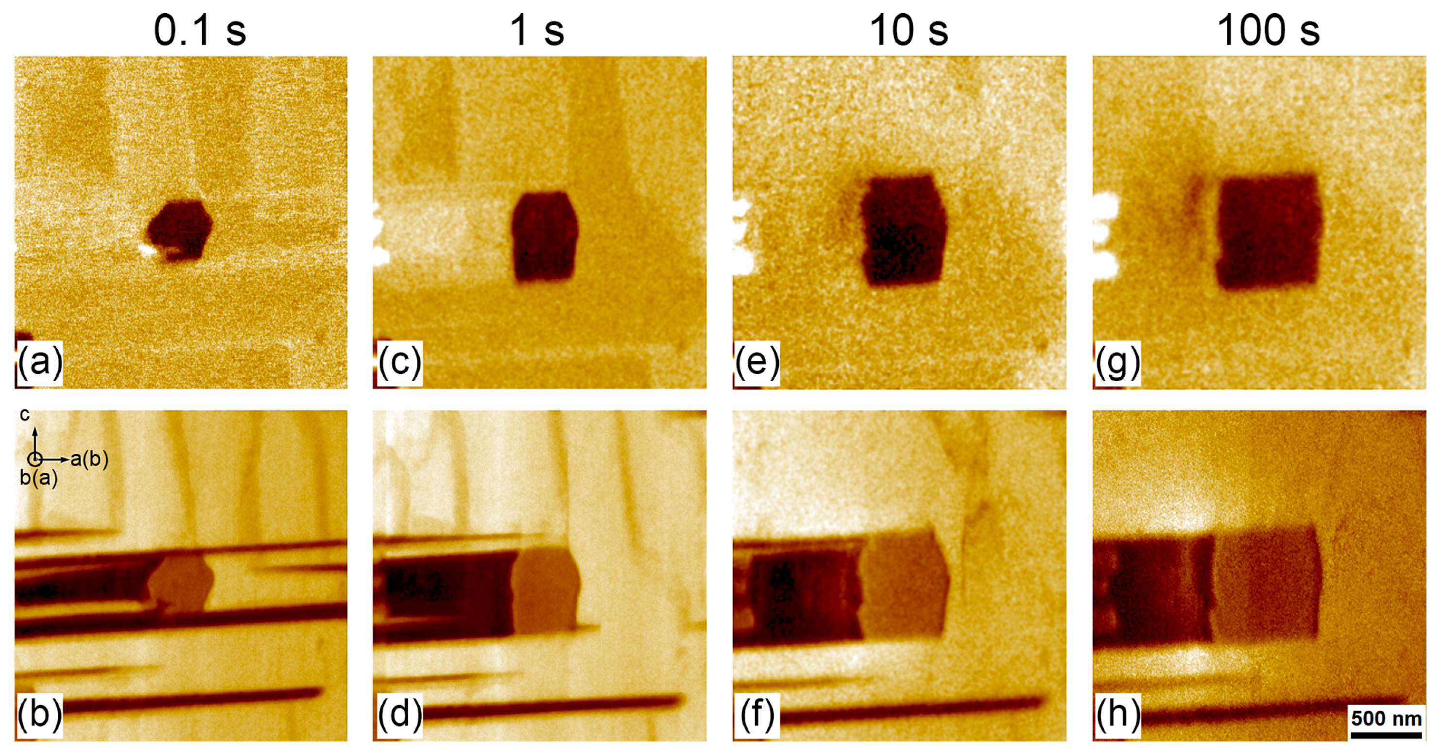
We measured the dependence of the domain size on pulse duration over a wide range of RHs for b-a switching, which occurs in multiaxial crystals only (Figure 5). The growth of wedge-like domains hampered the motion of the wall of hexagonal domains along the a-axis. Therefore, we analyzed the size evolution of the hexagonal domain along the c-axis only.
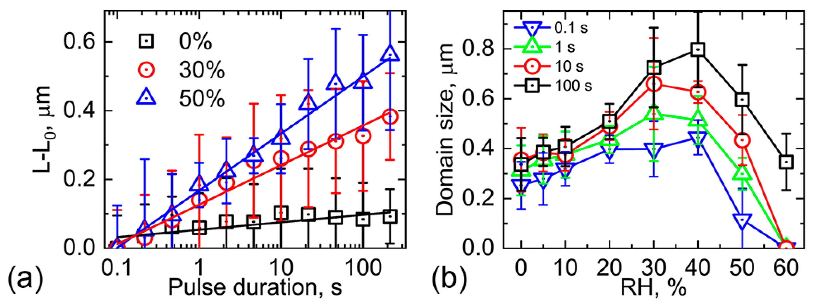
We measured the dependence of the domain size along the c-axis at different humidities on pulse durations ranging from 100 ms to 464 s for a fixed applied voltage of Usw = 50 V. It was shown that the increase in the domain size occurred with pulse durations over 1 s (Figure 6). In contrast, the size of the minimal domain that appeared after applying a 100 ms pulse is about 350 nm for all humidities below 40% (Figure 6b). This sharp decrease was observed at a RH above 40% (Figure 6b). Similar behavior, obtained earlier for local switching in lithium niobate, was attributed to the influence of the water meniscus [47].
The obtained logarithmic dependence of the increase in domain size along the c-axis on the pulse duration is typical for ferroelectric crystals (Figure 6a) [64].

4. Discussion

In terms of a kinetic approach, the domain-structure evolution during local switching is realized by the appearance of a nucleus of varying dimensionality under the action of the polar component of the spatially nonuniform and time-dependent electric field Eloc [38]. Domain wall motion is realized through the formation of the steps at the wall and the motion of kinks along the wall [38]. New domains represent 3D nuclei, steps on the domain walls (2D nuclei), and charged kinks (step edges)—1D nuclei.
In an initial single-domain state, the depolarization field produced by bound charges is completely compensated by slow bulk screening. This effect manifests itself in the formation of the bias field Eb, leading to a shift of the hysteresis loop [65]. The wall motion under application of an external voltage is limited by fast external screening of the appeared depolarization field by the current between polar surfaces.
The domain wall motion velocity is proportional to the excess of Eloc over the threshold field value for step generation Eth [66]:
v D W E = μ   Δ E l o c ,           Δ E l o c > 0                       0 ,             Δ E l o c < 0
where μ is wall mobility, Δ E l o c = E l o c E t h .
Eloc consists of four inputs: (1) Etip is the external field produced by the SPM tip, (2) Edep is the depolarization field produced by bound charges in the switched area and dependent on the domain size and shape, (3) Eex.scr is the external screening field governed by fast charge redistribution at the electrodes, and (4) Eb is the bias field created by bulk screening produced by several slow bulk processes [67].
E l o c r , t = E t i p r , t E d e p r , t E e x . s c r r , t E b
In the case of step-by-step switching, the time interval between subsequent switching events is much longer than the characteristic time of bulk screening, and the depolarization field of the switched domain is completely screened. Thus, during the application of a switching pulse, the depolarization field is created by bound charges located in a narrow area of the growing domain with width equal to domain shift Δ x s ; this is screened by fast external screening:
E l o c Δ x s , t > E t h
After termination of the field pulse and withdrawal of the conductive tip, the reversed wall motion (spontaneous backswitching) started under the action of Eb.
E l o c . b s r , t = E b E d e p Δ x b s , t E e x . s c r Δ x b s , t E b > E t h
where Δ x b s is the wall shift during backwitching.

4.1. a-a Switching

The dependence of the domain size on the pulse duration for domain growth along the b-axis during a-a switching was considered in terms of anisotropic current-limited domain wall motion (Figure 4e). The following formula for the time dependence of the domain size along the b-axis was used for fitting the experimental data [54]:
L t s w = L 0 + A b   t s w 1 / 2
where L is the domain length, L0 is the initial domain length, A b = 2 ( U s w U t h ) 1 / 2 / ( ρ b P s ) 1 / 2 , Uth is the threshold voltage for domain wall motion, ρb is the conductivity along the b-axis, and Ps is the spontaneous polarization. L0 corresponds to the sizes of a domain rapidly switched in high fields in the vicinity of the tip.
The best-fit values were L0 = 0.6 ± 0.1 μm, Ab = 0.06 ± 0.01 μm·s−1/2.
The obtained dependence of the domain size on the pulse duration for domain growth along the c-axis with low conductivity is typical for domain growth during local switching [64,68]:
L t s w = k   l n ( t s w / τ )
where k is the coefficient and τ is the characteristic time.

4.2. b-a Switching

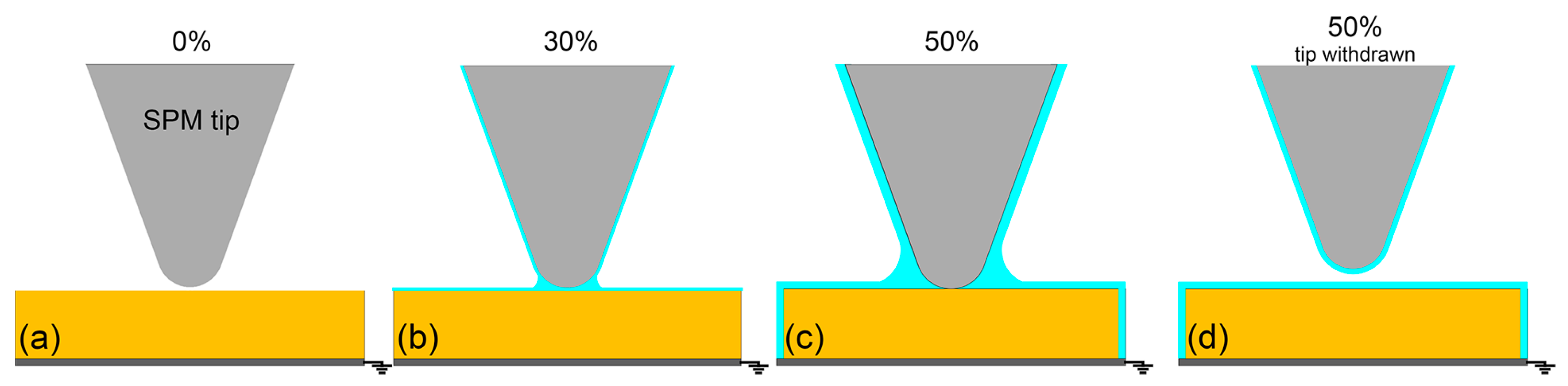
The domain wall motion along the c-axis with low bulk conductivity is limited by surface screening, which depends on RH. The surface conductivity is determined by the thickness of the adsorbed water layer [50]. Thus, an increase in RH essentially changes the domain growth during local switching [47,48]. Three RH ranges can be distinguished depending on their influence on domain growth: (i) at RH < 20%, the conductivity of the extremely thin discontinuous water layer is negligible (Figure 7a) [50], (ii) at RH 20–40%, the conductive water meniscus appears at the tip (Figure 7b), (iii) at RH > 40%, the whole surface of the sample, including the sides, is covered by a high-resistivity water layer (Figure 7c) [50,51].
The water meniscus appears at moderate humidity and acts as a top electrode, increasing the contact between the tip and the sample. This fact leads to delocalization of the external field produced by the biased SPM tip and to an increase in the domain size with humidity at RH < 40% [47,54,69] (Figure 6b).
The decrease in the domain sizes with humidity at RH > 40% can be attributed to spontaneous backswitching [57] over several minutes between the end of the switching pulse with tip withdrawal and domain imaging (Figure 7d). In this case, the presence of a high-resistivity water layer on the side surfaces of the sample facilitated backswitching under the action of the residual depolarization field Erd. The screening of the depolarization field, appearing during backward motion of the domain wall, is realized by leakage current across the water layer, which demonstrates a significant increase with RH [50,51].
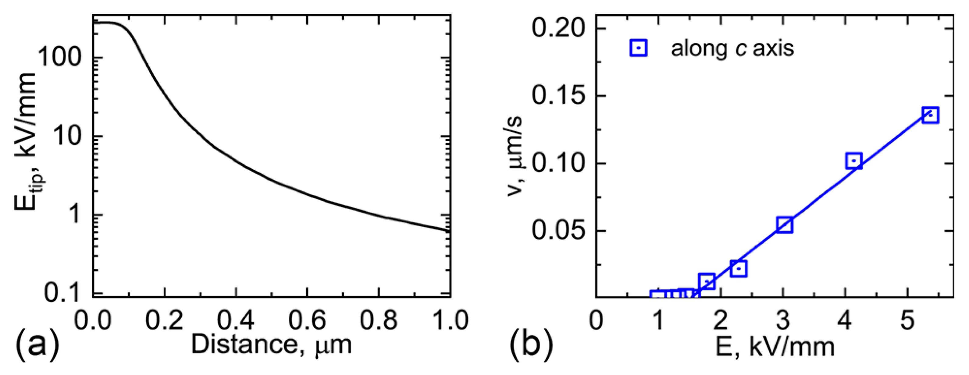
The finite element method in the COMSOL Multiphysics software (version 5.3) package was used to calculate the electric field distribution at the sample surface created by the biased conductive SPM tip. The computational model represented a cylindrical sample and a conical conductive SPM probe with a flat contact pad of 35 nm radius. The dielectric constants εa = 120, εb = 205, and εc = 140 were used [11]. The boundary conditions set the potential on the tip and zero potential at the outer boundary of the computational volume, realized by a layer of “infinite” elements. The simulated dependence of Etip on the distance from the tip was calculated for a water meniscus with a radius of 100 nm, corresponding to RH = 30% [48] (Figure 8a).
The dependences of domain-wall velocity were obtained as the derivative of the domain-size dependence along the c-axis on the pulse duration (Figure 6a and Figure S3). The electric field in which the domain wall moves decreases rapidly with distance (Figure 8a). The electric field produced by the SPM tip was calculated using COMSOL. Fitting the field dependence of domain wall velocity (Figure S4b) by Equation (1) allowed us to obtain Eth = 1.5 ± 0.2 kV/mm (Figure 8b), which is close to the value measured by macroscopic hysteresis loops [33].

5. Conclusions

We studied the as-grown domain structure and the growth of isolated domains during local switching by a biased SPM tip on a (100) cut of bismuth titanate Bi4Ti3O12 single crystal. The as-grown domain structure consists of two domain types: a-type (out-of-plane) and b-type (in-plane). Both types contain lamellar domain structures with submicron periods down to 50 nm. Local switching of the a-type domain area leads to the formation of a hexagonal a-type domain (a-a switching) with 180° walls. Local switching of the b-type domain area leads to the formation of a hexagonal a-type domain (b-a switching) with 90° walls and a b-type wedge-shaped domain with 180° domain walls and a length up to several microns. The growth of wedge-like domains hampered the wall motion of hexagonal ones along the a-axis. The sizes of a-type domains increase linearly with applied voltage. In the case of a-a switching, strong growth anisotropy was observed with increasing pulse duration. Domain growth along the c-axis is significantly slower than along the a-axis. The dependence of the domain size on the pulse duration for domain growth along the b-axis was considered in terms of anisotropic current-limited domain wall motion. The growth anisotropy was attributed to the known anisotropy of bulk conductivity. In the case of b-a switching, the dependence of the domain size along the c-axis on the pulse duration was measured over a wide range of RHs. For all RH values, a logarithmic dependence was obtained, typical of ferroelectric crystals. The increase in domain size at moderate humidity was attributed to the influence of the water meniscus acting as the top electrode. The decrease in domain size at high humidity was attributed to the influence of the conductive water layer. The presence of such a layer on the side surfaces of the sample facilitated backswitching under the action of the residual depolarization field. The screening of the depolarization field arising during backward motion of the domain wall is realized by leakage current, which demonstrates a significant increase with increasing RH. The presented technique of studying domain kinetics with high spatial resolution under application of the local fields allows extracting important information on domain-structure evolution in ferroelectrics with C2 symmetry and can facilitate the proper development of domain-engineering methods.

Supplementary Materials

The following supporting information can be downloaded at: https://www.mdpi.com/article/10.3390/cryst16050315/s1, Figure S1: PFM images of the isolated domain created by local a-a switching: (a) just after switching, (b) after 48 h. Usw = 100 V, tsw = 1 s. RH = 30%.; Figure S2: Scheme of the simulated tip and sample geometries; Figure S3: (a) Dependences of domain size along c axis on pulse duration for various humidities. Dependences of domain wall velocity for RH = 30% on (b) pulse duration and (c) distance from the tip. Usw = 50 V.; Figure S4: Simulated spatial distributions of the polar components of electric field: (a) vertical, (b) lateral. (c) field dependence of the domain wall motion velocity along c-axis. Voltage 50 V.

Author Contributions

Conceptualization, A.T., M.K. and V.S.; methodology, A.T. and V.S.; software, M.K. and S.M.; investigation, A.T.; resources, V.S.; writing—original draft preparation, A.T. and V.S.; writing—review and editing, A.T. and V.S.; visualization, A.T. and S.M.; supervision, V.S.; project administration, V.S. All authors have read and agreed to the published version of the manuscript.

Funding

The research was made possible by the Russian Science Foundation (Project No. 24-72-00170).

Data Availability Statement

The raw data supporting the conclusions of this article will be made available by the authors on request.

Acknowledgments

The equipment of the Ural Center for Shared Use “Modern nanotechnology” Ural Federal University (Reg. No. 2968) was used. The authors are grateful to V.M. Skorikov (Kurnakov Institute of General and Inorganic Chemistry, Moscow, Russia) for providing the crystals.

Conflicts of Interest

The authors declare no conflicts of interest.

Abbreviations

The following abbreviations are used in this manuscript:
RHRelative humidity
TGSTriglycine sulphate
KTPPotassium titanyl-phosphate
PFMPiezoresponse force microscopy
BiTBismuth titanate
FeRAMFerroelectric Random Access Memory

References

  1. Sirleto, L.; Righini, G.C. An Introduction to Nonlinear Integrated Photonics Devices: Nonlinear Effects and Materials. Micromachines 2023, 14, 604. [Google Scholar] [CrossRef] [Scilit]
  2. Liu, X.; Liu, Y.; Chen, W.; Li, J.; Liao, L. Ferroelectric Memory Based on Nanostructures. Nanoscale Res. Lett. 2012, 7, 285. [Google Scholar] [CrossRef] [Scilit] [PubMed]
  3. Setter, N.; Damjanovic, D.; Eng, L.; Fox, G.; Gevorgian, S.; Hong, S.; Kingon, A.; Kohlstedt, H.; Park, N.Y.; Stephenson, G.B.; et al. Ferroelectric Thin Films: Review of Materials, Properties, and Applications. J. Appl. Phys. 2006, 100, 051606. [Google Scholar] [CrossRef] [Scilit]
  4. Scott, J.F.; Paz de Araujo, C.A. Ferroelectric Memories. Science 1989, 246, 1400–1405. [Google Scholar] [CrossRef] [Scilit]
  5. Cummins, S.E.; Cross, L.E. Electrical and Optical Properties of Ferroelectric Bi4Ti3O12 Single Crystals. J. Appl. Phys. 1968, 39, 2268–2274. [Google Scholar] [CrossRef] [Scilit]
  6. Moure, A.; Castro, A.; Pardo, L. Aurivillius-Type Ceramics, a Class of High Temperature Piezoelectric Materials: Drawbacks, Advantages and Trends. Prog. Solid State Chem. 2009, 37, 15–39. [Google Scholar] [CrossRef] [Scilit]
  7. Chen, H.; Shen, B.; Xu, J.; Zhai, J. The Grain Size-Dependent Electrical Properties of Bi4Ti3O12 Piezoelectric Ceramics. J. Alloys Compd. 2013, 551, 92–97. [Google Scholar] [CrossRef] [Scilit]
  8. Watanabe, H.; Mihara, T.; Yoshimori, H.; de Araujo, C.A.P. Preparation of Ferroelectric Thin Films of Bismuth Layer Structured Compounds. Jpn. J. Appl. Phys. 1995, 34, 5240. [Google Scholar] [CrossRef] [Scilit]
  9. Ferrara, M.C.; Montecchi, M.; Mittiga, A.; Schioppa, M.; Mazzarelli, S.; Tapfer, L.; Lovergine, N.; Prete, P. Synthesis and Annealing Effects on Microstructure and Optical Properties of Wide-Bandgap Polycrystalline Ferro-Pseudobrookite FeTi2O5 Sol-Gel Layers. Ceram. Int. 2025, 51, 9669–9676. [Google Scholar] [CrossRef] [Scilit]
  10. Naciri, Y.; Hsini, A.; Ahdour, A.; Akhsassi, B.; Fritah, K.; Ajmal, Z.; Djellabi, R.; Bouziani, A.; Taoufyq, A.; Bakiz, B.; et al. Recent Advances of Bismuth Titanate Based Photocatalysts Engineering for Enhanced Organic Contaminates Oxidation in Water: A Review. Chemosphere 2022, 300, 134622. [Google Scholar] [CrossRef] [Scilit]
  11. Wu, J.; Qin, N.; Lin, E.; Yuan, B.; Kang, Z.; Bao, D. Synthesis of Bi4Ti3O12 Decussated Nanoplates with Enhanced Piezocatalytic Activity. Nanoscale 2019, 11, 21128–21136. [Google Scholar] [CrossRef] [Scilit] [PubMed]
  12. Moure, A. Review and Perspectives of Aurivillius Structures as a Lead-Free Piezoelectric System. Appl. Sci. 2018, 8, 62. [Google Scholar] [CrossRef] [Scilit]
  13. Suárez, D.Y.; Reaney, I.M.; Lee, W.E. Origin of Ferroelectricity in Aurivillius Compounds. MRS Online Proc. Libr. 2001, 658, 119. [Google Scholar] [CrossRef] [Scilit]
  14. Peña, M.A.; Fierro, J.L.G. Chemical Structures and Performance of Perovskite Oxides. Chem. Rev. 2001, 101, 1981–2018. [Google Scholar] [CrossRef] [Scilit] [PubMed]
  15. Taylor, G.W. Utilization of the t* Partial Switching Properties of Ferroelectrics in Memory Devices. IEEE Trans. Electron. Comput. 1965, EC-14, 881–886. [Google Scholar] [CrossRef] [Scilit]
  16. Chon, U.; Jang, H.M.; Kim, M.G.; Chang, C.H. Layered Perovskites with Giant Spontaneous Polarizations for Nonvolatile Memories. Phys. Rev. Lett. 2002, 89, 087601. [Google Scholar] [CrossRef] [Scilit]
  17. Supriya, S. Tailoring Layered Structure of Bismuth-Based Aurivillius Perovskites: Recent Advances and Future Aspects. Coord. Chem. Rev. 2023, 479, 215010. [Google Scholar] [CrossRef] [Scilit]
  18. Chen, H.; Shen, Z.; Guo, W.-T.; Jiang, Y.-P.; Li, W.; Zhang, D.; Tang, Z.; Sun, Q.-J.; Tang, X.-G. Artificial Synaptic Simulating Pain-Perceptual Nociceptor and Brain-Inspired Computing Based on Au/Bi3.2La0.8Ti3O12/ITO Memristor. J. Mater. 2024, 10, 1308–1316. [Google Scholar] [CrossRef] [Scilit]
  19. Yin, S.-F.; Sun, Q.-J.; Liu, L.-F.; Liu, S.-Z.; Jiang, Y.-P.; Tang, X.-G. TiO2/Bi4Ti3O12 Heterojunction Optoelectronic Synaptic Devices for Simulating Associative Memory and Neuromorphic Computation. Appl. Surf. Sci. 2025, 711, 164049. [Google Scholar] [CrossRef] [Scilit]
  20. Urushihara, D.; Komabuchi, M.; Ishizawa, N.; Iwata, M.; Fukuda, K.; Asaka, T. Direct Observation of the Ferroelectric Polarization in the Layered Perovskite Bi4Ti3O12. J. Appl. Phys. 2016, 120, 142117. [Google Scholar] [CrossRef] [Scilit]
  21. Chakraborty, K.R.; Achary, S.N.; Patwe, S.J.; Krishna, P.S.R.; Shinde, A.B.; Tyagi, A.K. Low Temperature Neutron Diffraction Studies on Bi4Ti3O12. Ceram. Int. 2007, 33, 601–604. [Google Scholar] [CrossRef] [Scilit]
  22. Xie, S.; Shi, J.; Xu, Q.; Wang, Q.; Zhu, J.; Sato, Y.; Chen, Q. In-Depth Understanding of {110}-Type Domain Walls in Bismuth Titanate Ceramics. Scr. Mater. 2022, 217, 114793. [Google Scholar] [CrossRef] [Scilit]
  23. Soga, M.; Noguchi, Y.; Miyayama, M.; Okino, H.; Yamamoto, T. Domain Structure and Polarization Properties of Lanthanum-Substituted Bismuth Titanate Single Crystals. Appl. Phys. Lett. 2004, 84, 100–102. [Google Scholar] [CrossRef] [Scilit]
  24. Xie, S.; Chen, Y.; Liu, W.; Xia, G.; Huang, B.; Liu, C.; Wang, Q.; Li, J. Three-Dimensional Domain Patterns in Tetragonal-to-Monoclinic Bi4Ti3O12 Ceramics: Nonlinear Analysis and Piezoresponse Force Microscopy Imaging. Acta Mater. 2020, 188, 228–240. [Google Scholar] [CrossRef] [Scilit]
  25. Kitanaka, Y.; Noguchi, Y.; Miyayama, M. Oxygen-Vacancy-Induced 90–Domain Clamping in Ferroelectric Bi4Ti3O12 Single Crystals. Phys. Rev. B 2010, 81, 094114. [Google Scholar] [CrossRef] [Scilit]
  26. Arlt, G.; Sasko, P. Domain Configuration and Equilibrium Size of Domains in BaTiO3 Ceramics. J. Appl. Phys. 1980, 51, 4956–4960. [Google Scholar] [CrossRef] [Scilit]
  27. Huffman, M.; Zhu, J.; Al-Jassim, M.M. Morphology and Domain Structure of Ferroelectric Lead Titanate and Lead Zirconate Titanate Thin Films, an Overview. Ferroelectrics 1993, 140, 191–201. [Google Scholar] [CrossRef] [Scilit]
  28. Jiang, F.; Seiji, K.; Yang, Y.; Yin, Q. Domain Observation of Ferroelectric Bi4Ti3O12 and Ferroelastic NdP5O14 Single Crystals with Scanning Electron Acoustic Microscope. Ferroelectrics 1999, 222, 237–241. [Google Scholar] [CrossRef] [Scilit]
  29. Osada, M.; Tada, M.; Kakihana, M.; Noguchi, Y.; Miyayama, M. Observation of Ferroelectric Domains in Bismuth-Layer-Structured Ferroelectrics Using Raman Spectroscopy. Mater. Sci. Eng. B 2005, 120, 95–99. [Google Scholar] [CrossRef] [Scilit]
  30. Moure, A.; López-Sánchez, J.; del Campo, A.; Navarro-Rojero, M.G.; Fernández, J.F.; Rubio-Marcos, F. Ferroelectric Domain Structure in Bi4Ti3O12 Ceramics: Insights from Confocal Raman Microscopy. J. Eur. Ceram. Soc. 2024, 44, 7032–7039. [Google Scholar] [CrossRef] [Scilit]
  31. Jardiel, T.; Caballero, A.C.; Fernández, J.F.; Villegas, M. Domain Structure of Bi4Ti3O12 Ceramics Revealed by Chemical Etching. J. Eur. Ceram. Soc. 2006, 26, 2823–2826. [Google Scholar] [CrossRef] [Scilit]
  32. Ye, W.; Lu, C.; Zhang, Y.; Zhou, Y. Types and Configurations of Domain Walls in Ferroelectric Bi4Ti3O12 Single Crystals. J. Appl. Crystallogr. 2015, 48, 1080–1088. [Google Scholar] [CrossRef] [Scilit]
  33. Yamamoto, K.; Kitanaka, Y.; Suzuki, M.; Miyayama, M.; Noguchi, Y.; Moriyoshi, C.; Kuroiwa, Y. High-Oxygen-Pressure Crystal Growth of Ferroelectric Bi4Ti3O12 Single Crystals. Appl. Phys. Lett. 2007, 91, 162909. [Google Scholar] [CrossRef] [Scilit]
  34. Katayama, S.; Noguchi, Y.; Miyayama, M. 3D Domain Structure in Bi4Ti3O12 Crystals Observed by Using Piezoresponse Force Microscopy. Adv. Mater. 2007, 19, 2552–2555. [Google Scholar] [CrossRef] [Scilit]
  35. Kitanaka, Y.; Noguchi, Y.; Miyayama, M. Ferroelectric Domain Structure and c-Axis Polarization Switching in Monoclinic Bi4Ti3O12 Single Crystals. Appl. Phys. Lett. 2007, 90, 202904. [Google Scholar] [CrossRef] [Scilit]
  36. Iwata, M.; Morishita, T.; Aoyagi, R.; Maeda, M.; Ishibashi, Y. Polarization Reversal Process in Bi4Ti3O12 with 90° Domain Wall Structure. Ferroelectrics 2008, 368, 36–41. [Google Scholar] [CrossRef] [Scilit]
  37. Iwata, M.; Morishita, T.; Aoyagi, R.; Maeda, M.; Suzuki, I.; Ishibashi, Y. In Situ Observation of Polarization Reversal of Bi4Ti3O12 with 90° Domain Walls. Jpn. J. Appl. Phys. 2007, 46, 3485. [Google Scholar] [CrossRef] [Scilit]
  38. Shur, V.Y.; Pelegova, E.V.; Turygin, A.P.; Kosobokov, M.S.; Alikin, Y.M. Forward Growth of Ferroelectric Domains with Charged Domain Walls. Local Switching on Non-Polar Cuts. J. Appl. Phys. 2021, 129, 044103. [Google Scholar] [CrossRef] [Scilit]
  39. Bornarel, J. Textures in Natural Domains. In Ferroic Crystal Domains, Walls, and Phase Fronts; Bornarel, J., Ed.; Springer Nature: Cham, Switzerland, 2025; pp. 53–109. [Google Scholar] [CrossRef] [Scilit]
  40. Nakatani, N. Observation of Ferroelectric Domain Structure in TGS. Ferroelectrics 2011, 413, 238–265. [Google Scholar] [CrossRef] [Scilit]
  41. Akhmatkhanov, A.R.; Chuvakova, M.A.; Kipenko, I.A.; Dolgushin, N.A.; Kolker, D.B.; Vedenyapin, V.N.; Isaenko, L.I.; Shur, V.Y. Abnormal Kinetics of Domain Structure in KTA Single Crystals. Appl. Phys. Lett. 2019, 115, 212901. [Google Scholar] [CrossRef] [Scilit]
  42. Bolshakova, N.N.; Nekrasova, G.M.; Petrova, V.N.; Rudyak, V.M. Pyroelectric Properties and Domain Structure Realignment in Gadolinium Molybdate Single Crystals. Ferroelectrics 1991, 118, 35–39. [Google Scholar] [CrossRef] [Scilit]
  43. Kalinin, S.V.; Dyck, O.; Balke, N.; Neumayer, S.; Tsai, W.-Y.; Vasudevan, R.; Lingerfelt, D.; Ahmadi, M.; Ziatdinov, M.; McDowell, M.T.; et al. Toward Electrochemical Studies on the Nanometer and Atomic Scales: Progress, Challenges, and Opportunities. ACS Nano 2019, 13, 9735–9780. [Google Scholar] [CrossRef] [Scilit] [PubMed]
  44. Lu, W.; Zeng, K. Characterization of Local Electric Properties of Oxide Materials Using Scanning Probe Microscopy Techniques: A Review. Funct. Mater. Lett. 2018, 11, 1830002. [Google Scholar] [CrossRef] [Scilit]
  45. Miccoli, I.; Edler, F.; Pfnür, H.; Tegenkamp, C.; Prete, P.; Lovergine, N. Surface-Mediated Electrical Transport in Single GaAs Nanowires. In Proceedings of the 2015 1st Workshop on Nanotechnology in Instrumentation and Measurement (NANOFIM); IEEE: Lecce, Italy, 2015; Volume 1, pp. 136–140. [Google Scholar] [CrossRef] [Scilit]
  46. Kholkin, A.; Kalinin, S.; Roelofs, A.; Gruverman, A. Review of Ferroelectric Domain Imaging by Piezoresponse Force Microscopy. In Scanning Probe Microscopy Electrical and Electromechanical Phenomena at the Nanoscale; Kalinin, S., Gruverman, A., Eds.; Springer: New York, NY, USA, 2007; pp. 173–214. [Google Scholar] [CrossRef] [Scilit]
  47. Ievlev, A.V.; Morozovska, A.N.; Shur, V.Y.; Kalinin, S.V. Humidity Effects on Tip-Induced Polarization Switching in Lithium Niobate. Appl. Phys. Lett. 2014, 104, 092908. [Google Scholar] [CrossRef] [Scilit]
  48. Blaser, C.; Paruch, P. Subcritical Switching Dynamics and Humidity Effects in Nanoscale Studies of Domain Growth in Ferroelectric Thin Films. New J. Phys. 2015, 17, 013002. [Google Scholar] [CrossRef] [Scilit]
  49. Weeks, B.L.; Vaughn, M.W.; Deyoreo, J.J. Direct Imaging of Meniscus Formation in Atomic Force Microscopy Using Environmental Scanning Electron Microscopy. Langmuir 2005, 21, 8096–8098. [Google Scholar] [CrossRef] [Scilit]
  50. Lin, Y.-T.; Agnello, G.; Link, M.; Guo, Y.; Zoba, A.N.; Antony, A.; Smith, N.J.; Banerjee, J.; Kim, S.H. Water Adsorption Isotherm and Surface Conductivity of Boroaluminosilicate Glasses. Langmuir 2024, 40, 1658–1665. [Google Scholar] [CrossRef] [Scilit]
  51. Yang, L.; He, J.; Shen, Y.; Li, X.; Sun, J.; Czajkowsky, D.M.; Shao, Z. Nanoscopic Characterization of the Water Vapor-Salt Interfacial Layer Reveals a Unique Biphasic Adsorption Process. Sci. Rep. 2016, 6, 31688. [Google Scholar] [CrossRef] [Scilit] [PubMed]
  52. McGilly, L.J.; Feigl, L.; Setter, N. Domain Nucleation Behavior in Ferroelectric Films with Thin and Ultrathin Top Electrodes versus Insulating Top Layers. Thin Solid Films 2017, 636, 214–219. [Google Scholar] [CrossRef] [Scilit]
  53. McGilly, L.J.; Yudin, P.; Feigl, L.; Tagantsev, A.K.; Setter, N. Controlling Domain Wall Motion in Ferroelectric Thin Films. Nat. Nanotechnol. 2015, 10, 145–150. [Google Scholar] [CrossRef] [Scilit]
  54. Shishkina, E.V.; Pelegova, E.V.; Kosobokov, M.S.; Akhmatkhanov, A.R.; Yudin, P.V.; Dejneka, A.; Shur, V.Y. Influence of Humidity on Local Polarization Reversal in a Rb:KTP Single Crystal. ACS Appl. Electron. Mater. 2021, 3, 260–266. [Google Scholar] [CrossRef] [Scilit]
  55. Turygin, A.P.; Shikhova, V.A.; Kosobokov, M.S.; Akhmatkhanov, A.R.; Sergeeva, O.N.; Shur, V.Y. Highly Anisotropic Tip-Induced Domain Growth in Polydomain Triglycine Sulfate. ACS Appl. Electron. Mater. 2022, 4, 5215–5220. [Google Scholar] [CrossRef] [Scilit]
  56. Ievlev, A.V.; Alikin, D.O.; Morozovska, A.N.; Varenyk, O.V.; Eliseev, E.A.; Kholkin, A.L.; Shur, V.Y.; Kalinin, S.V. Symmetry Breaking and Electrical Frustration during Tip-Induced Polarization Switching in the Nonpolar Cut of Lithium Niobate Single Crystals. ACS Nano 2015, 9, 769–777. [Google Scholar] [CrossRef] [Scilit]
  57. Shur, V.Y.; Rumyantsev, E.L.; Nikolaeva, E.V.; Shishkin, E.I.; Fursov, D.V.; Batchko, R.G.; Eyres, L.A.; Fejer, M.M.; Byer, R.L. Nanoscale Backswitched Domain Patterning in Lithium Niobate. Appl. Phys. Lett. 2000, 76, 143–145. [Google Scholar] [CrossRef] [Scilit]
  58. Morrison, A.D.; Lewis, F.A.; Miller, A. The Growth of Large Single-Crystal Bi4Ti3O12. Ferroelectrics 1970, 1, 75–78. [Google Scholar] [CrossRef] [Scilit]
  59. Soergel, E. Piezoresponse Force Microscopy (PFM). J. Phys. D Appl. Phys. 2011, 44, 464003. [Google Scholar] [CrossRef] [Scilit]
  60. Alikin, D.; Turygin, A.; Ushakov, A.; Kosobokov, M.; Alikin, Y.; Hu, Q.; Liu, X.; Xu, Z.; Wei, X.; Shur, V. Competition between Ferroelectric and Ferroelastic Domain Wall Dynamics during Local Switching in Rhombohedral PMN-PT Single Crystals. Nanomaterials 2022, 12, 3912. [Google Scholar] [CrossRef] [Scilit] [PubMed]
  61. da Cunha Fernandes, T.; Ushakov, A.; Turygin, A.P.; Fabrelli, H.; Eiras, J.A.; Shur, V.Y.; Lente, M.H. As-Grown Domain Structure and Local Switching in [111]-Cut Cu-Doped KNN Single Crystals. J. Appl. Phys. 2025, 138, 184101. [Google Scholar] [CrossRef] [Scilit]
  62. Yi, I.-S.; Miyayama, M. Electrical Anisotropies in Layer-Structured Lead Bismuth Titanate Single Crystals. Mater. Res. Bull. 1997, 32, 1349–1357. [Google Scholar] [CrossRef] [Scilit]
  63. Kim, S.K.; Miyayama, M.; Yanagida, H. Electrical Anisotropy and a Plausible Explanation for Dielectric Anomaly of Bi4Ti3O12 Single Crystal. Mater. Res. Bull. 1996, 31, 121–131. [Google Scholar] [CrossRef] [Scilit]
  64. Agronin, A.; Molotskii, M.; Rosenwaks, Y.; Rosenman, G.; Rodriguez, B.J.; Kingon, A.I.; Gruverman, A. Dynamics of Ferroelectric Domain Growth in the Field of Atomic Force Microscope. J. Appl. Phys. 2006, 99, 104102. [Google Scholar] [CrossRef] [Scilit]
  65. Chynoweth, A.G. Radiation Damage Effects in Ferroelectric Triglycine Sulfate. Phys. Rev. 1959, 113, 159–166. [Google Scholar] [CrossRef] [Scilit]
  66. Shur, V.Y. Kinetics of Ferroelectric Domains: Application of General Approach to LiNbO3 and LiTaO3. J. Mater. Sci. 2006, 41, 199–210. [Google Scholar] [CrossRef] [Scilit]
  67. Merz, W.J. Domain Formation and Domain Wall Motions in Ferroelectric BaTiO3 Single Crystals. Phys. Rev. 1954, 95, 690–698. [Google Scholar] [CrossRef] [Scilit]
  68. Rodriguez, B.J.; Nemanich, R.J.; Kingon, A.; Gruverman, A.; Kalinin, S.V.; Terabe, K.; Liu, X.Y.; Kitamura, K. Domain Growth Kinetics in Lithium Niobate Single Crystals Studied by Piezoresponse Force Microscopy. Appl. Phys. Lett. 2005, 86, 012906. [Google Scholar] [CrossRef] [Scilit]
  69. Slautin, B.; Turygin, A.; Pashnina, E.; Slautina, A.; Chezganov, D.; Shur, V. Evolution of Nanodomains and Formation of Self-Organized Structures during Local Switching in X-Cut LNOI. Crystals 2022, 12, 659. [Google Scholar] [CrossRef] [Scilit]
Figure 1. (a) Scheme of the possible spontaneous polarization orientations in the a-cut BiT sample. PFM images of the initial domain structure: (b,e,h) out-of-plane and (c,f,i) in-plane piezoresponse; (e,f) are the marked zoomed regions at (b,c). (h,i) are the marked zoomed regions at (e,f). Schemes of domain orientations: (d) for (b,c), (g) for (e,f), and (j) for (h,i). Arrows ←/→ denote left/right Ps orientation, circles ⊙/⊗ denote inward/outward Ps orientation.
Crystals 16 00315 g001
Figure 2. PFM images of the domains created by local switching. (a) a-a switching, out-of-plane signal, (b) scheme. (c) b-a switching, in of-plane signal, (d) scheme. Usw = 100 V, tsw = 1 s. RH = 30%. Arrows ←/→ denote left/right Ps orientation, circles ⊙/⊗ denote inward/outward Ps orientation. Red dot indicates point of bias application.
Crystals 16 00315 g002
Figure 3. Out-of-plane PFM images of the domain created by local switching using pulse sequence with various voltages: (ac) a-a switching, (df) b-a switching. (g) Voltage dependence of the domain size along c-axis. Usw: (a,d) 50 V, (b,e) 150 V, (c,f) 200 V. tsw = 1 s. RH = 30%. Red dot indicates point of bias application.
Crystals 16 00315 g003
Figure 4. PFM images of domain evolution created by a-a local switching using pulse sequence with various durations: (a) 0.1 s, (b) 1 s, (c) 10 s, and (d) 100 s. (e) Dependence of the domain size on pulse duration. Usw = 50 V, RH = 30%. Red dot indicates point of bias application.
Crystals 16 00315 g004
Figure 5. PFM images of domain evolution as a result of b-a local switching by sequence of pulses with various durations for RH = 30%: (a,b) 0.1 s, (c,d) 1 s, (e,f) 10 s, and (g,h) 100 s. (a,c,e,g) Out-of-plane and (b,d,f,h) in-plane piezoresponses.
Crystals 16 00315 g005
Figure 6. Dependences of the following: (a) increase in the domain size along the c-axis at different humidities on pulse duration, (b) the domain size along the c-axis on humidity for different tsw. Usw = 50 V.
Crystals 16 00315 g006
Figure 7. Schemes of the sample with SPM tip and water layers for various RH values: (a) dry atmosphere, (b) 30%, (c) 50%, and (d) 50% after tip withdrawal.
Crystals 16 00315 g007
Figure 8. (a) Simulated dependence of Etip on the distance from the tip for a water meniscus with a radius 100 nm. (b) Field dependence of the domain wall motion velocity along the c-axis at RH = 30%. Usw = 50 V.
Crystals 16 00315 g008
Disclaimer/Publisher’s Note: The statements, opinions and data contained in all publications are solely those of the individual author(s) and contributor(s) and not of MDPI and/or the editor(s). MDPI and/or the editor(s) disclaim responsibility for any injury to people or property resulting from any ideas, methods, instructions or products referred to in the content.