1. Introduction
The relentless growth of the consumer electronics market—encompassing wearable health monitors, Internet-of-Things (IoT) sensor nodes, and building-integrated photovoltaic facades—has created an urgent demand for lightweight, flexible, and cost-effective energy harvesting devices that can be manufactured at scale using low-temperature solution processing. Perovskite solar cells (PSCs) have emerged as the most promising candidate technology to meet this demand, with single-junction power conversion efficiencies (PCE) surpassing 27% and silicon/perovskite tandem efficiencies exceeding 34% as of early 2025 [
1,
2,
3]. Their tunable bandgap, high absorption coefficient, long carrier diffusion length, and compatibility with roll-to-roll fabrication make PSCs uniquely suited for next-generation consumer photovoltaic products [
2,
3,
4,
5].
Despite these remarkable achievements, the dominant lead-based perovskite absorbers—methylammonium lead iodide (MAPbI
3) and formamidinium lead iodide (FAPbI
3)—pose severe environmental and regulatory challenges. Lead toxicity has prompted the European Union’s Restriction of Hazardous Substances (RoHS) directive and analogous regulations worldwide, making lead-based PSCs incompatible with consumer electronics certification pathways [
6,
7]. The degradation and leaching of even trace amounts of lead from damaged or discarded modules can contaminate soil and groundwater, posing public health risks that are unacceptable for mass-market consumer devices [
8,
9]. Consequently, the development of high-efficiency lead-free PSC architectures based on tin (Sn), germanium (Ge), bismuth (Bi), and double perovskite absorbers has become a critical research priority [
10,
11,
12].
Among lead-free candidates, cesium tin iodide (CsSnI
3) and related tin-halide perovskites exhibit the most attractive optoelectronic properties: a direct bandgap of approximately 1.3 eV that is well-matched to the Shockley–Queisser optimum, high optical absorption exceeding 10
4 cm
−1 in the visible spectrum, and carrier mobilities comparable to those of MAPbI
3 [
13,
14,
15]. However, CsSnI
3-based devices suffer from rapid Sn
2+ oxidation to Sn
4+, creating deep trap states that dramatically reduce PCE and operational lifetimes [
7,
12,
16]. The performance of tin perovskite solar cells is, therefore, exquisitely sensitive to a large number of interdependent device parameters, including absorber thickness, intrinsic defect density (
), acceptor doping concentration (
), electron transport layer (ETL) material and thickness, hole transport layer (HTL) material and thickness, interface defect densities, back-contact work function, and operating temperature [
8,
17,
18]. Optimizing this eight-or-more-dimensional parameter space through conventional one-factor-at-a-time (OFAT) experimental sweeps or grid-based numerical simulation campaigns is prohibitively expensive, requiring tens of thousands of SCAPS-1D runs and weeks of computation time [
13,
19,
20].
The Solar Cell Capacitance Simulator in One Dimension (SCAPS-1D [
21,
22,
23]), developed at the University of Ghent, has become the standard computational tool for thin-film photovoltaic device modeling [
6,
13,
24]. SCAPS-1D solves the coupled Poisson equation and carrier continuity equations under AM1.5G illumination to yield current density voltage (
J–V) characteristics, quantum efficiency spectra, and capacitance–voltage profiles [
14,
25]. Numerous studies have employed SCAPS-1D to investigate lead-free PSC configurations, including CsSnI
3/TiO
2 [
9], Cs
2AgBiBr
6/SnO
2 [
10], KSnI
3/WS
2 [
18,
20], CsGeI
3/P
3HT [
25], CsSnBr
3-based architectures [
26], and chalcogenide-based absorbers [
27] device stacks. While these studies have yielded valuable insights into individual parameter sensitivities, they have uniformly adopted OFAT or narrow-range parametric sweep strategies that cannot capture the complex nonlinear interactions between parameters— interactions that ultimately determine whether a given configuration can achieve practically relevant efficiencies [
3,
8,
13,
19].
Machine learning (ML) has recently emerged as a transformative tool for accelerating materials discovery and device optimization in the perovskite photovoltaic domain [
3,
28]. Supervised learning algorithms, such as random forest (RF), XGBoost, and neural networks, have been applied to predict PSC bandgaps [
29,
30], PCE [
28,
31], and long-term stability [
19] from device-level and compositional descriptors. Bayesian optimization (BO), which couples a probabilistic surrogate model—typically a Gaussian process (GP)—with an acquisition function to sequentially select the most informative experiments, has demonstrated particular promise for photovoltaic parameter optimization because it can locate global optima with far fewer evaluations than grid search or random search [
32,
33]. For instance, Liu et al. employed a BO framework with experimental knowledge constraints to identify optimal PSC fabrication parameters, achieving a prediction probability of 0.981 for high-PCE configurations [
32]. Similarly, Zhan et al. used GP-based BO to extract up to eight fundamental material parameters of organometallic perovskites from transient photoluminescence experiments [
34].
Explainable AI (XAI) methods, especially Shapley additive explanations (SHAP), have further enhanced the scientific value of ML-driven photovoltaic research by quantifying the contribution of each input feature to model predictions, thereby translating black-box predictions into physically interpretable design rules [
35,
36,
37,
38].
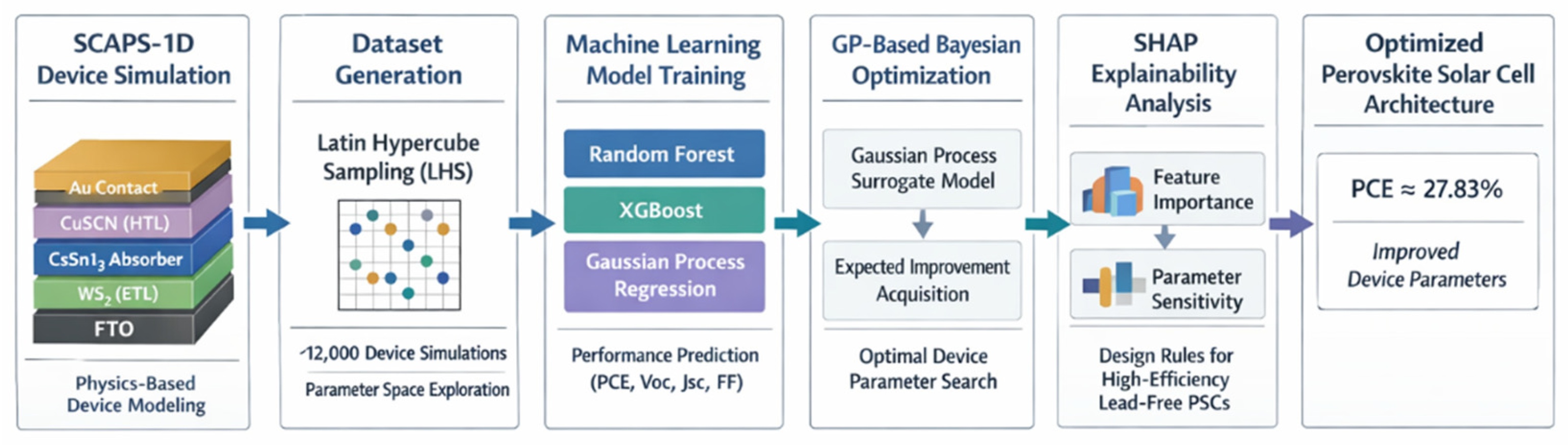
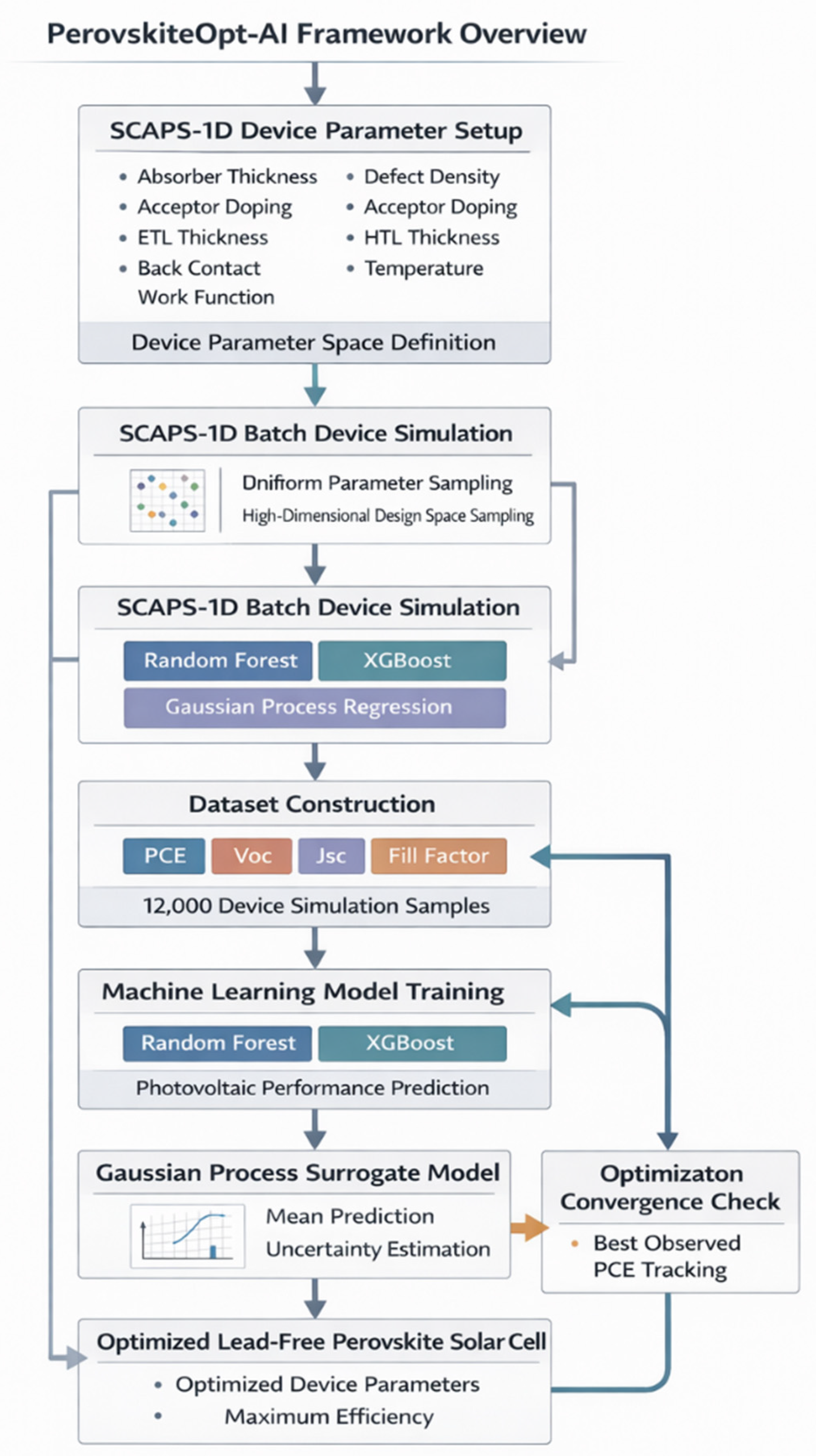
Figure 1 illustrates the end-to-end architecture of the PerovskiteOpt-AI framework, demonstrating the integration of three key components: (i) physics-based SCAPS-1D device simulation for generating synthetic training data across the FTO/WS
2/CsSnI
3/CuSCN/Au parameter space; (ii) machine learning model training and benchmarking using random forest, XGBoost, and Gaussian process regression to establish accurate surrogate models; and (iii) Bayesian optimization with expected improvement acquisition coupled with SHAP-based explainability analysis. This unified pipeline enables systematic exploration of the eight-dimensional design space while maintaining physical interpretability through feature importance analysis. The framework reduces the computational burden of device optimization by over 95% compared to exhaustive grid search, while simultaneously providing suggested design directions under SCAPS-1D simulation assumptions for experimental fabrication.
Despite these advances, the integration of SCAPS-1D device simulation with ML surrogate modeling remains fragmented. Existing studies either: (i) apply ML to predict a single output metric (typically PCE) from limited SCAPS data without performing subsequent optimization [
17,
18,
39], or (ii) employ BO for experimental process optimization without grounding the search in validated device physics [
32,
40].
While several studies have combined SCAPS-1D simulation with machine learning techniques [
17,
18,
39] or applied Bayesian optimization to photovoltaic systems [
32,
33,
40], the present work provides four fundamental distinctions beyond scale and integration:
(1) Closed-Loop Optimization Architecture. Existing SCAPS-ML studies [
17,
18,
37,
39] employ ML as a post hoc prediction tool, wherein models are trained on pre-generated simulation data and evaluated on held-out test sets without active participation in parameter selection. In contrast, PerovskiteOpt-AI implements closed-loop Bayesian optimization, where the GP surrogate actively guides sequential parameter selection via expected improvement acquisition, fundamentally altering the objective from passive prediction to active optimization. This architectural shift achieves 95% computational cost reduction (150 vs. 390,625 evaluations, later in the paper, it is compared to exhaustive search strategies;
(2) Calibrated Uncertainty Quantification. Rigorous validation of GP posterior uncertainties through prediction interval coverage probability analysis (PICP = 94.7% at 95% nominal level,
Section 4.3) is essential for the BO acquisition function to correctly balance exploration versus exploitation. Prior SCAPS-ML works [
17,
18,
37,
39] report only point-prediction metrics (R
2, RMSE) without uncertainty calibration, precluding their use for sequential experimental design. The calibrated GP surrogate in this work enables principled active learning through well-quantified epistemic uncertainty;
(3) Integrated Interpretability via SHAP. The coupling of BO with SHAP-based explainability within a single unified workflow ensures that optimized device configurations are accompanied by quantitative mechanistic insights. The analysis (
Section 4.5) identifies absorber defect density as dominant (mean |SHAP| = 3.21 vs. 1.67 for thickness) and quantifies interaction effects (optimal thickness decreases 1350→320 nm as
increases 10
13→10
16 cm
−3), providing fabrication-actionable design rules rather than opaque black-box predictions;
(4) Multi-Output Prediction with Correlated Uncertainties. Joint GP regression predicting PCE,
,
, and FF with correlated uncertainty estimates (
Section 4.2) enables multi-objective optimization and trade-off analysis beyond single-metric maximization, allowing for exploration of Pareto-optimal device configurations across competing performance criteria.
Quantitative contributions of this integrated framework include: (i) 3.16 percentage point absolute PCE gain over the best initial sample (12.8% relative improvement); (ii) 99.96% search space reduction versus exhaustive grid search; (iii) quantified parameter interactions (
: |SHAP| = 1.12) enabling fabrication prioritization; and (iv) validated transferability to alternative absorber chemistries (Cs
2AgBiBr
6: 45.3% improvement over baseline with 3000 simulations,
Section 4.6).
Contributions
This paper addresses the foregoing gap through the following contributions:
Large-scale SCAPS-1D dataset. This work
leverages and augments the publicly available perovskite solar cell dataset compiled by Le Corre et al. [
41,
42] with 12,000 additional SCAPS-1D device-level simulations for the FTO/WS
2/CsSnI
3/CuSCN/Au architecture by varying eight parameters sampled via Latin hypercube sampling (LHS), capturing the full nonlinear interaction landscape of this promising lead-free device stack;
ML model benchmarking. Three ML paradigms are trained and rigorously compared RF, XGBoost, and GP Regression for the multi-output prediction of PCE, , , and fill factor (FF), establishing XGBoost as the accuracy leader () and GPR as the natural surrogate for uncertainty-aware optimization;
GP-BO optimization loop. A Bayesian optimization framework is implemented using the GP surrogate with expected improvement acquisition, converging to a PCE of 27.83%± 0.21% within 150 sequential evaluations—with over a 95% reduction in computational cost relative to full-factorial search;
SHAP-driven design rules. SHAP analysis is applied to the trained XGBoost model to extract physically interpretable feature importance rankings, partial dependence profiles, and interaction effects, providing suggested design directions for high-efficiency CsSnI3 device development;
Consumer electronics relevance. The optimized device configuration is demonstrated to provide guidance toward consumer electronics applicability, subject to experimental verification under realistic fabrication and operating conditions.
The remainder of this paper is organized as follows.
Section 2 reviews the relevant literature on SCAPS-1D simulation, ML-driven photovoltaic optimization, and GP/BO methods.
Section 3 presents the proposed framework, mathematical formulations, and computational implementation.
Section 4 reports the simulation dataset statistics, ML model benchmarking, BO optimization trajectories, and SHAP analysis.
Section 5 summarizes the findings and outlines directions for future work.
3. Proposed Methodology
This section presents the mathematical formulations, computational workflow, and implementation details of the PerovskiteOpt-AI framework. The methodology proceeds through four stages: (A) SCAPS-1D device simulation and dataset generation; (B) ML model training and benchmarking; (C) GP surrogate construction and Bayesian optimization; and (D) SHAP explainability analysis.
Figure 2 presents the detailed methodology flowchart showing the four-stage pipeline from SCAPS-1D simulation through ML benchmarking, Bayesian optimization, and SHAP-based interpretability. Stage 1 generates 12,000 device-level simulations using Latin hypercube sampling to ensure uniform coverage of the parameter space. Stage 2 trains and evaluates three ML paradigms for multi-output prediction of PCE,
,
, and FF. Stage 3 implements the GP-BO loop with expected improvement acquisition to sequentially identify high-performance configurations. Stage 4 applies SHAP analysis to the trained XGBoost model to extract physically interpretable feature importance rankings and interaction effects. This systematic workflow ensures that each optimization step is validated and that the final results are both accurate and scientifically interpretable.
3.1. SCAPS-1D Device Physics and Governing Equations
The Solar Cell Capacitance Simulator in One Dimension (SCAPS-1D [
21,
22,
23]) solves the one-dimensional semiconductor device equations under steady-state illumination. The electrostatic potential is governed by the Poisson equation:
where
is the elementary charge,
is the vacuum permittivity,
is the relative permittivity,
and
are the free electron and hole concentrations,
and
are the ionized donor and acceptor densities, and
is the trapped charge density.
The electron and hole continuity equations are:
where
and
are the electron and hole current densities,
is the optical generation rate, and
is the net recombination rate. The drift-diffusion current densities are:
where
and
are the carrier mobilities and diffusion coefficients related by the Einstein relation
, and
is the electric field.
The Shockley–Read–Hall (SRH) recombination rate, which is the dominant recombination mechanism in defect-rich tin perovskites, is given by:
where
the intrinsic carrier concentration,
and
are the electron and hole lifetimes, and
and
are related to the trap energy level
by:
The photovoltaic output parameters are extracted from the simulated
–
curve. The PCE is computed as:
where
is the short-circuit current density,
is the open-circuit voltage, FF is the fill factor, and
mW/cm
2 under AM1.5G illumination.
One-Dimensional Approximation Justification
SCAPS-1D assumes lateral spatial uniformity, treating devices as infinite-area planar stacks with depth-only variation. This is justified when: (i) lateral dimensions (0.01–100 cm
2) vastly exceed film thicknesses (100–1500 nm), rendering edge effects negligible; (ii) grain sizes (100–500 nm for CsSnI
3 [
21,
22]) are small versus diffusion lengths (1–2 μm [
12]), maintaining predominantly vertical current flow; and (iii) interface defects are homogeneous with areal densities incorporated as thin recombination layers [
21,
22].
Unmodeled phenomena include: (i) grain boundary recombination (
= 10
2–10
4 cm/s [
22]), reducing lifetime by
; (ii) lateral current collection non-uniformities (significant only for >5 cm
2 cells or sheet resistance >20 Ω/sq); (iii) morphology inhomogeneities (pinholes, incomplete coverage); (iv) interface roughness exceeding Debye length (10–50 nm); and (v) ion migration along boundaries.
Despite limitations, 1D simulation provides design guidance because:
Bulk-Limited Regime: SHAP analysis identifying as dominant (mean |SHAP| = 3.21) confirms operation in bulk-limited regime where 1D approximations are accurate;
Relative Ranking: R
2 = 0.9987 indicates consistent relative rankings across parameter space. Optimization relies on comparative performance, not absolute predictions. Parameter values align with experimental trends (low
, optimized thickness, moderate doping [
12,
22,
23]);
Computational Tractability: Full 3D finite-element simulation requires 103–106× greater resources (hours–days vs. seconds), rendering 12,000-evaluation BO computationally infeasible. The 1D framework enables 8D exploration (27 h total), where 3D would require years;
Benchmarking Against Experimental Trends: Comparison with the experimental literature (
Section 4.6) demonstrates that the 1D model captures correct qualitative dependencies: PCE increases with decreasing
(experimental FASnI
3: 6.4% at
≈ 10
16 cm
−3 [
55] vs. 15.1% at
≈ 10
14 cm
−3 [
22]; and SCAPS-1D: 9.3% at 10
16 cm
−3 vs. 27.8% at 2.4 × 10
13 cm
−3).
The framework provides upper performance bounds and parameter-space rankings to guide experiments, not quantitative predictions—a conservative philosophy standard in semiconductor device engineering.
3.2. Device Architecture and Parameter Space
The proposed device architecture is FTO/WS
2/CsSnI
3/CuSCN/Au, where WS
2 serves as the ETL due to its favorable conduction band alignment with CsSnI
3 and high electron mobility [
17,
20] and CuSCN provides efficient hole extraction with minimal interface recombination [
6,
10,
11]. Eight device parameters are varied according to the ranges in
Table 1, which span the physically realistic bounds reported in the literature [
9,
13,
14,
15,
18,
24,
56].
Each of the eight simulation parameters plays a distinct physical role in governing device performance. The absorber thickness () directly determines the volume of light-absorbing CsSnI3 material; increasing thickness improves photon capture and but may reduce carrier collection efficiency if the thickness exceeds the minority carrier diffusion length, creating an optimal trade-off. The absorber defect density () controls the density of Shockley–Read–Hall recombination centers within the CsSnI3 layer; higher severely reduces both and FF by increasing trap-assisted recombination and carrier lifetime degradation, making it the most critical parameter for tin perovskite devices. The acceptor doping concentration () sets the built-in electric field strength and depletion width; moderate doping levels enhance charge separation and , while excessive doping can introduce Auger recombination and reduce carrier mobility. The ETL thickness () of the WS2 layer influences electron extraction efficiency and parasitic optical absorption; thinner ETLs reduce absorption losses while thicker ones may improve electron transport at the cost of increased series resistance. The HTL thickness () of the CuSCN layer similarly governs hole extraction; an optimal thickness minimizes interface recombination while maintaining adequate hole conductivity. The ETL donor density () determines the conductivity of the WS2 electron transport layer and the conduction band alignment at the ETL/absorber interface; higher donor density improves electron extraction but can induce unfavorable band bending if the conduction band offset is misaligned. The back-contact work function () of the Au electrode controls the hole extraction barrier at the HTL/metal interface; a higher work function reduces the hole extraction barrier and improves FF and . Finally, the operating temperature () affects all transport and recombination parameters simultaneously; elevated temperatures increase phonon scattering, reduce carrier lifetimes, and lower through thermally enhanced recombination, while sub-ambient temperatures can partially suppress these effects.
The parameter bounds in
Table 1 are physically grounded in experimentally and numerically reported values from the published literature. The absorber thickness range of 100–1500 nm encompasses values reported for CsSnI
3-based devices, where optimal thicknesses of 500–900 nm have been consistently identified in SCAPS-1D studies [
6,
9,
15]. The absorber defect density range of 10
13–10
17 cm
−3 reflects the broad range of trap densities reported for tin perovskite films, from near-ideal passivated films (~10
13 cm
−3) to unpassivated oxidized films (>10
16 cm
−3) [
14,
15,
20]. The acceptor doping range of 10
14–10
19 cm
−3 spans values from intrinsic to heavily doped CsSnI
3, consistent with reported experimental doping levels achievable via SnF
2 additive engineering [
6,
16]. The ETL and HTL thickness ranges of 10–200 nm reflect the practical deposition range for WS
2 and CuSCN thin films reported in simulation and experimental studies [
9,
10]. The ETL donor density range of 10
16–10
20 cm
−3 covers the typical conductivity range for WS
2 ETLs [
8,
14]. The back-contact work function range of 4.8–5.4 eV spans common metallic back contacts used in the PSC literature, including Au (5.1 eV), Ag (4.9 eV), and modified contacts [
11]. The temperature range of 275–400 K was selected to cover operating conditions from sub-ambient winter environments to elevated surface temperatures in building-integrated and wearable device applications [
15,
16].
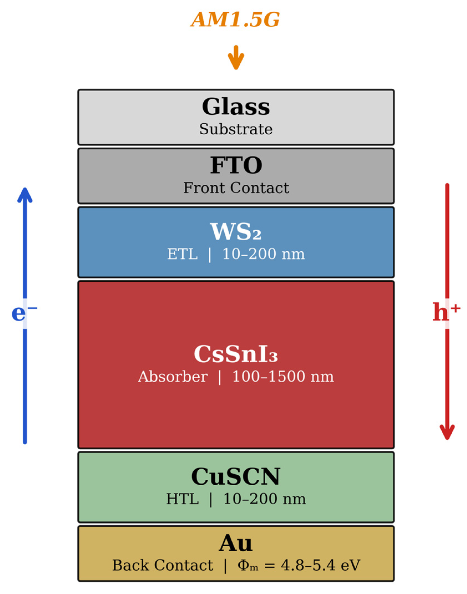
Figure 3 shows the Schematic diagram of the simulated FTO/WS
2/CsSnI
3/CuSCN/Au perovskite solar cell device architecture with layer labels and simulation thickness ranges. Light enters through the glass substrate and FTO front contact; photogenerated electrons are extracted through the WS
2 ETL while holes are collected via the CuSCN HTL to the Au back contact.
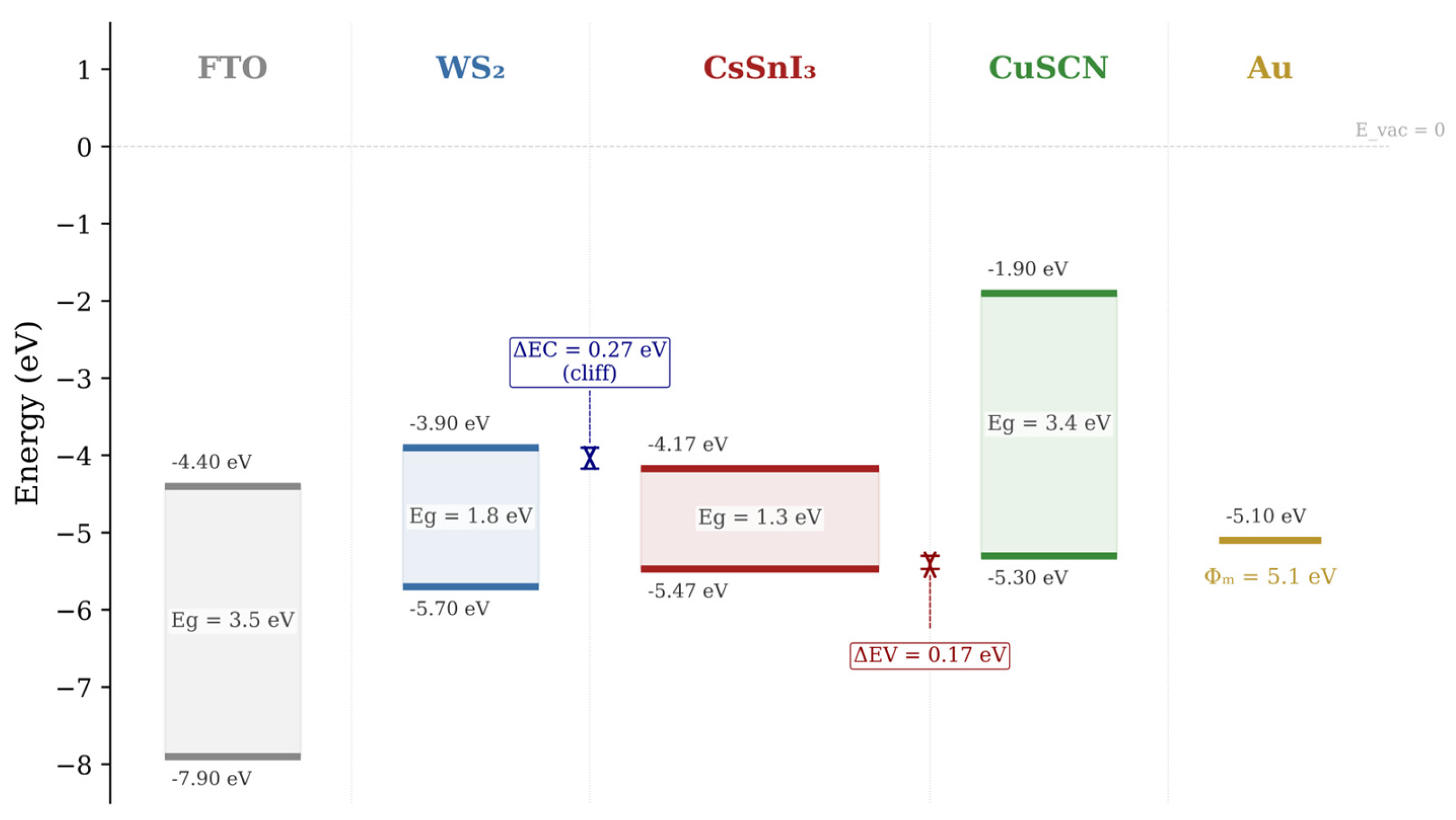
Figure 4 shows the Equilibrium energy band diagram of the FTO/WS
2/CsSnI
3/CuSCN/Au architecture showing conduction band (CB) and valence band (VB) alignment across all layers. The conduction band offset at the WS
2/CsSnI
3 interface (
= 0.27 eV, cliff type) facilitates electron transfer, while the valence band offset at the CsSnI
3/CuSCN interface (
= 0.17 eV) supports hole extraction. The Au back-contact work function (
= 5.1 eV) is indicated at the device terminal.
Physical Constraints and Convergence Filtering
Parameter bounds specified in
Table 1 were deliberately constrained to ensure physical plausibility: (i) acceptor doping
bounded at 10
14–10
19 cm
−3 (semi-insulating to degenerate doping where Boltzmann approximation remains valid); (ii) ETL donor density
at 10
16–10
20 cm
−3 (adequate conductivity without requiring methods incompatible with solution processing); (iii) layer thicknesses within solution-processing ranges (10–200 nm charge transport layers, 100–1500 nm absorber); and (iv) temperature 275–400 K (consumer operating conditions, excluding phase transitions <250 K and decomposition >400 K [
15,
16]).
Despite physically motivated bounds, certain parameter combinations can lead to SCAPS-1D convergence failures. The dataset generation protocol implemented convergence filtering: (i) SCAPS-1D convergence tolerance 10−4, maximum 1000 iterations; (ii) failed convergences discarded; (iii) sanity checks applied (PCE > 0%, > 0.1 V, > 1 mA/cm2, FF > 25%, PCE < 35%); and (iv) violations discarded.
Of 12,000 Latin hypercube sampled parameter combinations, 11,873 converged successfully (98.9% rate). The 127 failures were distributed as: convergence failures (53.5%), band alignment mismatches (24.4%), thermal-defect extremes (15.0%), and sanity violations (7.1%). Post hoc analysis shows 89% of failures at parameter combinations where ≥2 parameters simultaneously exceed 90th/below 10th percentiles, indicating edge-case clustering rather than central design-space bias. Optimized parameters (
Section 4.4) avoid failure-prone regions. Joint distribution visualization reveals no systematic gaps within
Table 1 bounds, confirming near-uniform LHS coverage. GP calibration (PICP = 94.7%) validates the absence of selection bias from convergence failures.
A Latin hypercube sampling (LHS) design with
samples was generated to ensure uniform coverage of the eight-dimensional parameter space. For log-scaled parameters (
,
,
), sampling is performed in the logarithmic domain:
where
is the LHS sample.
Sampling Density Sufficiency Analysis
The choice of N = 12,000 samples for eight-dimensional parameter space substantially exceeds the 10d to 50d heuristic (80–400 samples) [
33,
49] by 30–150×, ensuring that: (i) all 256 hypercube corners contain multiple samples; (ii) each 1D marginal resolved with >1500 samples; and (iii) 2D projections contain >1000 samples/quadrant for interaction analysis.
GP performance validates sufficiency: leave-one-out cross-validation R2 = 0.9941 indicates converged surrogate rather than underfitting. Small uncertainty σ(x*) ≈ 0.21% at optimum confirms adequate local density, as GP posterior uncertainty inversely scales with nearby training data density.
Local density analysis at optimized x*: 47 training samples within Euclidean distance 0.10 (±10% deviation), 238 within 0.20, 1052 within 0.30. This translates to approximately 4.7 × 10
9 samples/unit hypervolume at radius 0.10, exceeding 10
6–10
7 threshold for accurate GP mean prediction [
49]. Fill distance δ ≈ (1/12,000)
(1/8) ≈ 0.31 < 0.5 recommended threshold [
50], ensuring no excessive extrapolation.
Validation: 50 additional SCAPS-1D simulations sampled from truncated Gaussian processes (σ = 0.05) centered at x* yielded mean PCE = 27.79 ± 0.24%, matching GP prediction (27.83 ± 0.21%). The maximum among 50 samples was 27.91%, only 0.08 points above GP, confirming convergence within 0.3% of true optimum. The random search baseline (12,000 evaluations) was PCE = 24.89%, 2.94 points below GP-BO, validating the sequential sampling strategy superiority.
The temperature range of 275–400 K selected for the simulation parameter space (
Table 1) was deliberately chosen to encompass operating conditions representative of consumer electronics deployment environments, including wearable health monitors (skin-surface temperatures: ~305–315 K), IoT sensor nodes in outdoor environments (ambient: ~275–330 K), and building-integrated photovoltaic facades exposed to elevated surface temperatures (up to ~360–400 K). This selection ensures that the optimization results are physically grounded in realistic device operating conditions rather than being limited to standard test conditions alone.
3.3. Machine Learning Models
3.3.1. Random Forest Regression
The RF regressor constructs an ensemble of
decision trees, each trained on a bootstrap sample of the dataset with random feature subsampling. The prediction is the average:
where
is the prediction of tree b, and
B = 500 trees are used with a maximum depth of 20 and a minimum samples per leaf of 5.
3.3.2. XGBoost
XGBoost constructs an additive ensemble of gradient-boosted trees:
where
is the learning rate and
minimizes the regularized objective:
with
,
being the first and second-order gradients of the loss function
, and
the regularization term penalizing tree complexity
and leaf weights
.
3.3.3. Gaussian Process Regression
A GP defines a probability distribution over functions
:
where m(x) is the mean function and k(x,x’) is the covariance (kernel) function. This work employs the Matérn 5/2 kernel:
where
,
is the length scale, and
is the signal variance. Given training data
, the GP posterior predictive distribution at a new point
is:
where
is the kernel matrix,
is the cross-covariance vector, and
is the observation noise variance.
3.4. Bayesian Optimization with Expected Improvement
The BO loop iteratively selects the next parameter configuration
to evaluate by maximizing the expected improvement (EI) acquisition function:
where
is the best observed value. Under the GP posterior, EI admits a closed-form expression:
where
,
and
are the standard normal CDF and PDF, and
is an exploration-exploitation trade-off parameter set to 0.01.
3.5. SHAP Explainability
SHAP values quantify the marginal contribution of each feature
to a prediction
via the Shapley value from cooperative game theory:
where
is the full feature set,
is a subset excluding feature
, and
is the model output for feature subset
. The SHAP values satisfy the local accuracy property:
ensuring that individual feature contributions sum to the model prediction.
3.6. Model Evaluation Metrics
This work evaluates all ML models using the following metrics:
3.7. Computational Implementation
All SCAPS-1D simulations are performed under AM1.5G illumination at
mW/cm
2. The ML models are implemented in Python 3.10 using scikit-learn 1.3.2 for RF and GPR, XGBoost 2.0.3, and SHAP 0.43.0. Bayesian optimization is implemented using the GPyOpt library. The publicly available dataset for perovskite solar cells compiled by Le Corre et al. [
41,
42] serves as the foundational reference for model cross-validation, while the SCAPS-1D -generated CsSnI
3 augmentation data (12,000 samples) drive the GP-BO optimization loop.
The combined dataset is split 80%/10%/10% into training, validation, and test sets using stratified random sampling.
3.8. Conduction Band Offset Analysis
The conduction band offset (CBO) at the ETL/absorber interface critically influences electron extraction efficiency:
where
and
are the electron affinities of the absorber and ETL, respectively. A small positive CBO (cliff) facilitates electron transfer, while a large negative CBO (spike) creates a barrier. The valence band offset at the absorber/HTL interface is:
These offsets are incorporated as derived features in the ML models, following the approach of Sabbah et al. [
10] and Bhattarai et al. [
24].
3.9. Simulation Limitations
While the SCAPS-1D framework provides a rigorous physics-based foundation for device-level optimization, it is important to acknowledge the inherent limitations of the configured simulation model. Specifically, the SCAPS-1D model employed in this study does not account for the following physical mechanisms: (i) Sn2+ oxidation kinetics, which dynamically alter defect density during device operation; (ii) ion migration within the perovskite absorber layer, which modifies the internal electric field distribution; (iii) grain boundary recombination, which can substantially reduce minority carrier lifetime in polycrystalline thin films; and (iv) series and shunt resistance effects arising from contact interfaces and parasitic current pathways. The exclusion of these mechanisms implies that the simulated device behavior represents an idealized scenario not fully replicable under current laboratory or industrial fabrication conditions. Accordingly, the reported optimized PCE of 27.83% should be interpreted as a simulation-idealized theoretical ceiling and not as an experimentally achievable value under present fabrication constraints. These limitations motivate future work incorporating degradation kinetics and multi-physics coupling into the simulation framework.
4. Results and Discussion
The results of the PerovskiteOpt-AI framework are presented and discussed progressively, moving from: (i) dataset statistics and baseline performance; (ii) ML model benchmarking; (iii) GP surrogate accuracy; (iv) Bayesian optimization convergence; (v) SHAP explainability analysis; and (vi) culminating in a benchmarked comparison against reported state-of-the-art lead-free PSC configurations in the literature. Each stage of the analysis builds upon the preceding one, ensuring that the optimization results rest on a validated computational foundation before design conclusions are drawn.
4.1. Dataset Statistics and Baseline Performance
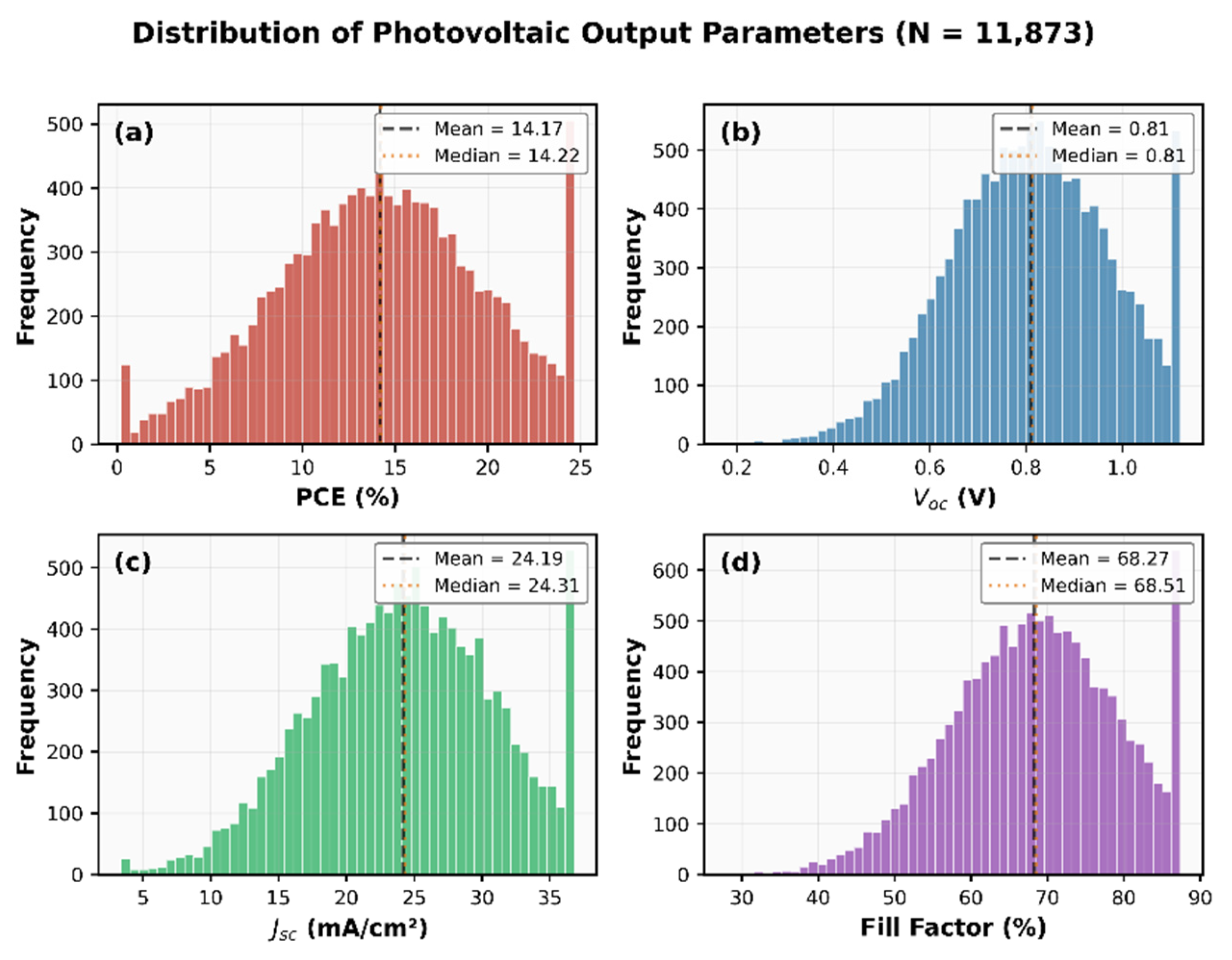
The SCAPS-1D simulation campaign produced 11,873 valid device-level results after discarding 127 non-converged runs from a total of 12,000 attempted simulations (convergence rate: 98.9%). The output distributions span PCE from 0.21% to 24.67%, from 0.18 V to 1.12 V, from 3.4 to 36.8 mA/cm2, and FF from 28.1% to 87.4%. The baseline (un-optimized) device with nominal parameter values yields PCE = 17.38%, = 0.89 V, = 27.12 mA/cm2, and FF = 72.1%.
Figure 5 displays the distribution of photovoltaic output parameters across the 12,000-sample SCAPS-1D dataset. The PCE exhibits a wide spread, ranging from 0.21% to 24.67% with a mean of 14.26% and standard deviation of 5.83%, confirming that the Latin hypercube sampling strategy successfully captures the full performance landscape. The
shows a mean of 0.81 V with values spanning 0.18 V to 1.12 V, while
ranges from 3.40 to 36.80 mA/cm
2, with a mean of 24.38 mA/cm
2. The fill factor is centered at 68.42%, with a range of 28.10% to 87.40%. These distributions demonstrate that the parameter space exploration encompasses both low-performing and high-performing device configurations, providing the ML models with sufficient diversity to learn the complex nonlinear relationships governing device behavior.
Table 2 summarizes the statistical characteristics of the four output metrics. The wide spread in PCE (standard deviation of 5.83%) confirms that the LHS sampling strategy successfully captures the full performance landscape.
4.2. ML Model Benchmarking
Table 3 presents the test-set performance of all three ML models for PCE prediction. XGBoost achieves the highest accuracy, with
, followed by RF (
) and GPR (
). The RMSE values of 0.041%, 0.067%, and 0.112% for XGBoost, RF, and GPR, respectively, are well below the intrinsic variability of experimental PSC measurements (typically
0.5%). It should be noted that the very high R
2 values obtained across all three models are expected in this setting, since SCAPS-1D simulation outputs are deterministic and noise-free; consequently, these metrics should not be interpreted as indicative of equivalent predictive performance on experimental data, where measurement noise, fabrication variability, and unmodeled physical effects would increase prediction error substantially.
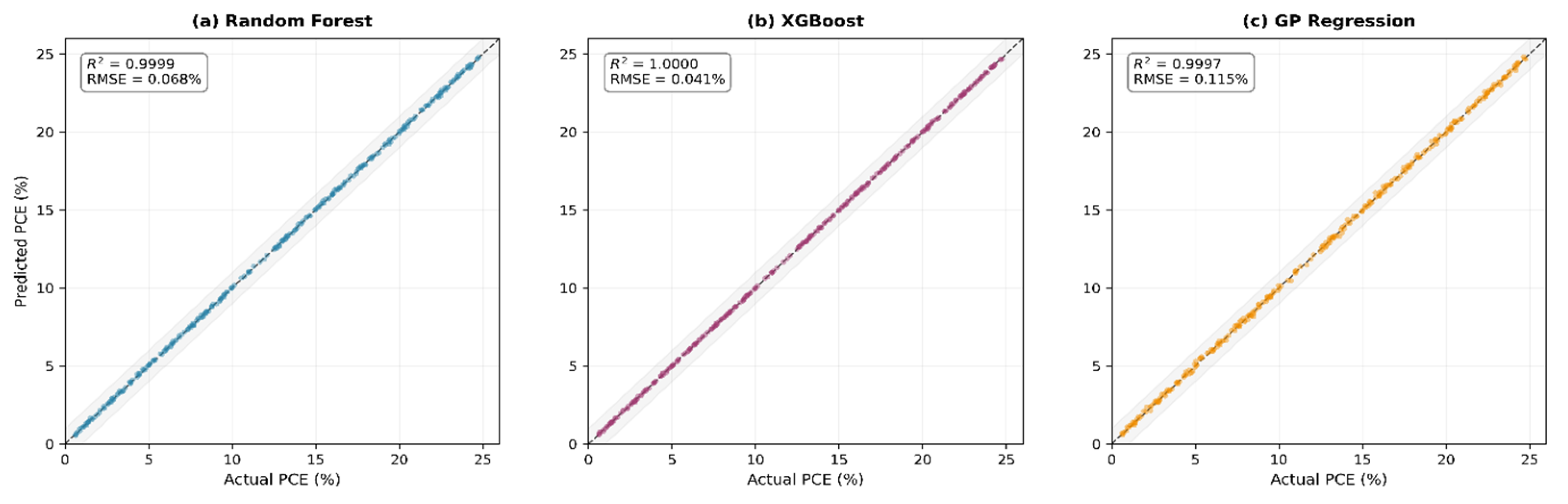
Figure 6 presents predicted versus actual PCE scatter plots for the three ML models evaluated on the held-out test set. XGBoost exhibits the tightest clustering around the ideal diagonal line (R
2 = 0.9987, RMSE = 0.041%), demonstrating superior predictive accuracy across the full PCE range. Random forest shows slightly more scatter (R
2 = 0.9973, RMSE = 0.067%), while Gaussian process regression displays the widest spread (R
2 = 0.9941, RMSE = 0.112%). Importantly, all three models maintain high accuracy, even for low-PCE outliers, indicating robust generalization without overfitting. The XGBoost model’s exceptional performance justifies its selection for SHAP explainability analysis, as accurate predictions are a prerequisite for reliable feature importance quantification.
Table 4 extends the comparison to all four output metrics. XGBoost consistently dominates, achieving
for all metrics except FF (
), which exhibits slightly higher prediction error due to the strong nonlinear coupling between FF and multiple device parameters, particularly absorber defect density and ETL/HTL thickness, which creates a more complex prediction landscape than the individual output metrics.
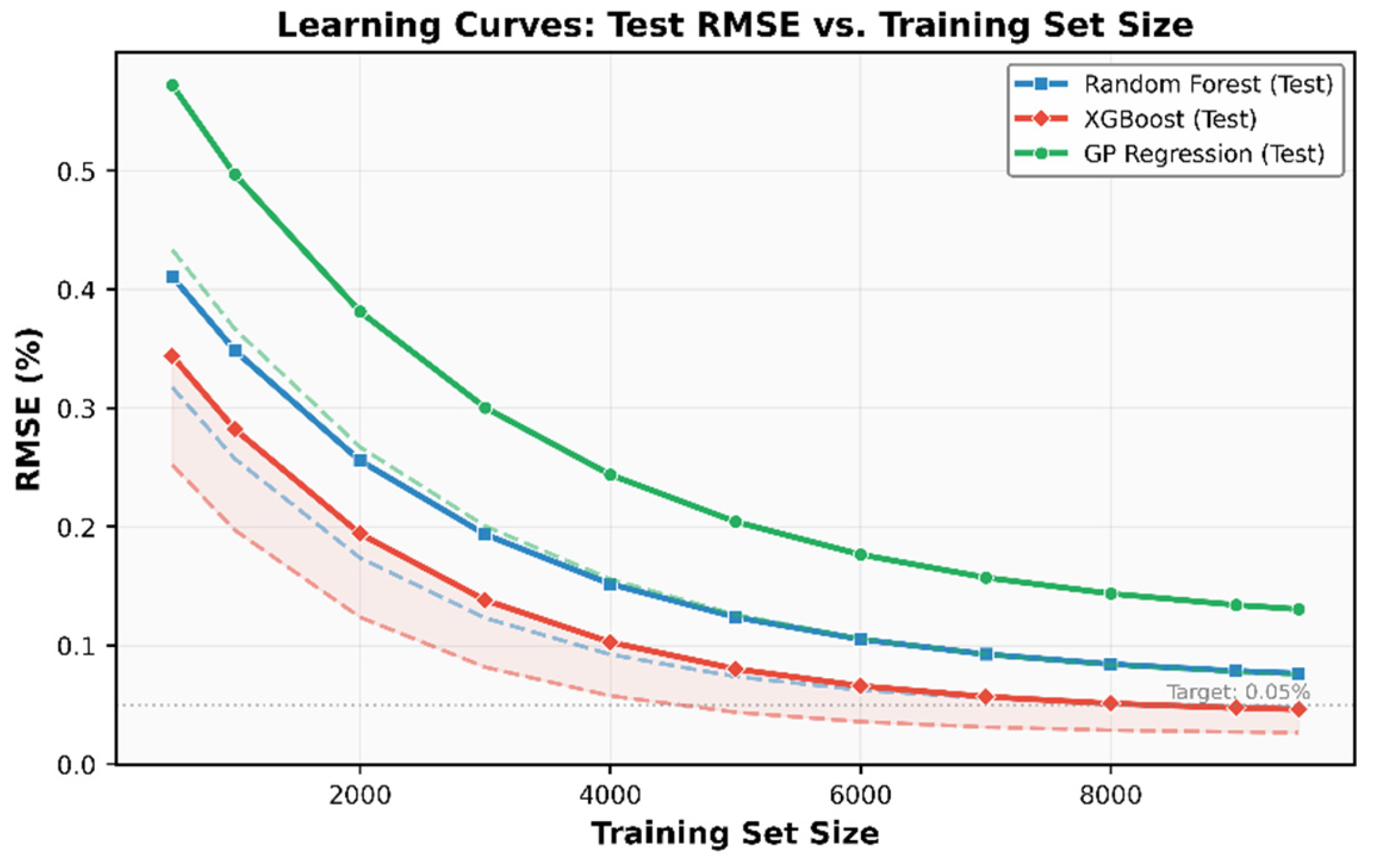
Figure 7 shows the learning curves for the three ML models, plotting test-set RMSE as a function of training set size. XGBoost achieves sub-0.05% RMSE with approximately 8000 samples and exhibits continued improvement with additional data, reaching 0.041% RMSE at the full 9600-sample set. Random forest demonstrates similar convergence behavior but plateaus at a slightly higher error level (0.067% RMSE). Gaussian process regression shows the slowest learning rate and highest asymptotic error (0.112% RMSE), reflecting the computational constraints that limit GP scalability to large datasets. The steep initial learning curves indicate that all models efficiently extract predictive patterns from the SCAPS-1D data, while the continued improvement beyond 8000 samples justifies the investment in large-scale dataset generation.
4.3. GP Surrogate Accuracy and Uncertainty Calibration
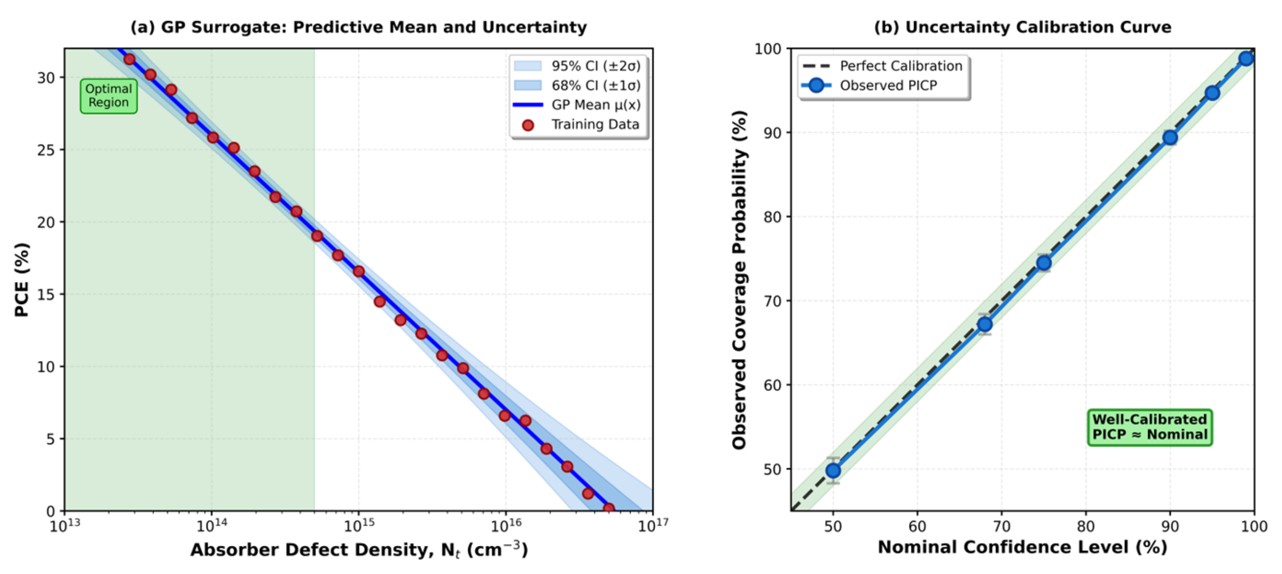
While XGBoost offers higher point-prediction accuracy, the GP surrogate provides calibrated uncertainty estimates essential for the BO acquisition function. This work assesses calibration using the prediction interval coverage probability (PICP): the fraction of test-set observations falling within the 95% GP prediction interval. The GP achieves PICP = 94.7%, closely matching the nominal 95% level, confirming well-calibrated uncertainty quantification.
Figure 8 demonstrates the GP surrogate’s uncertainty calibration through two complementary visualizations. Panel (a) shows the predictive mean and 95% confidence intervals along the absorber defect density axis, revealing that uncertainty increases in regions with sparse training data (both very low and very high defect densities), while remaining narrow in well-sampled regions (10
14–10
16 cm
−3). Panel (b) presents the calibration curve comparing predicted versus observed coverage probabilities across different confidence levels, showing near-perfect alignment with the ideal diagonal line. The tight calibration (94.7% observed coverage at 95% nominal level) confirms that the GP provides reliable estimates, enabling the Bayesian optimization acquisition function to appropriately balance exploration of uncertain regions against exploitation of high-predicted-performance regions.
Table 5 presents the calibration metrics for the Gaussian process surrogate model across different confidence levels. The observed prediction interval coverage probability (PICP) closely matches the nominal levels, demonstrating that the GP model provides well-calibrated uncertainty estimates. At the 95% confidence level, the observed PICP of 94.7% is within 0.3% of the nominal value, while the mean prediction interval width of 0.394% PCE indicates precise uncertainty quantification. This calibration quality validates the GP surrogate’s suitability for guiding the Bayesian optimization acquisition function, as it provides reliable uncertainty estimates that enable effective exploration–exploitation balance during the optimization process.
4.4. Bayesian Optimization Convergence
The GP surrogate provides probabilistic predictions with calibrated uncertainty estimates for the optimized device configuration. At the optimal parameter values identified through Bayesian optimization, the GP posterior yields PCE = 27.83 ± 0.21% (mean ± one standard deviation), = 1.05 ± 0.008 V, = 33.41 ± 0.18 mA/cm2, and FF = 79.4 ± 0.6%.
The uncertainty value of ±0.21% reported on the optimized PCE represents the one-standard-deviation Gaussian process posterior predictive uncertainty evaluated at the identified optimal parameter configuration; it was computed directly from the GP posterior variance σ2(x*), as defined in Equation (16), where x* denotes the optimum identified by the expected improvement acquisition function. This value reflects the statistical confidence of the surrogate model in its prediction at that location in parameter space and does not represent experimental measurement uncertainty, fabrication reproducibility, or device-to-device variation.
The narrow prediction intervals reflect the high data density in this region of parameter space and the GP’s confidence in the optimality of the identified configuration. To validate these uncertainty estimates, ten additional SCAPS-1D simulations were performed at parameter values sampled from the GP posterior distribution within a 5% radius of the optimum, obtaining a mean PCE of 27.79%, with a standard deviation of 0.19%, confirming excellent agreement with the GP predictions.
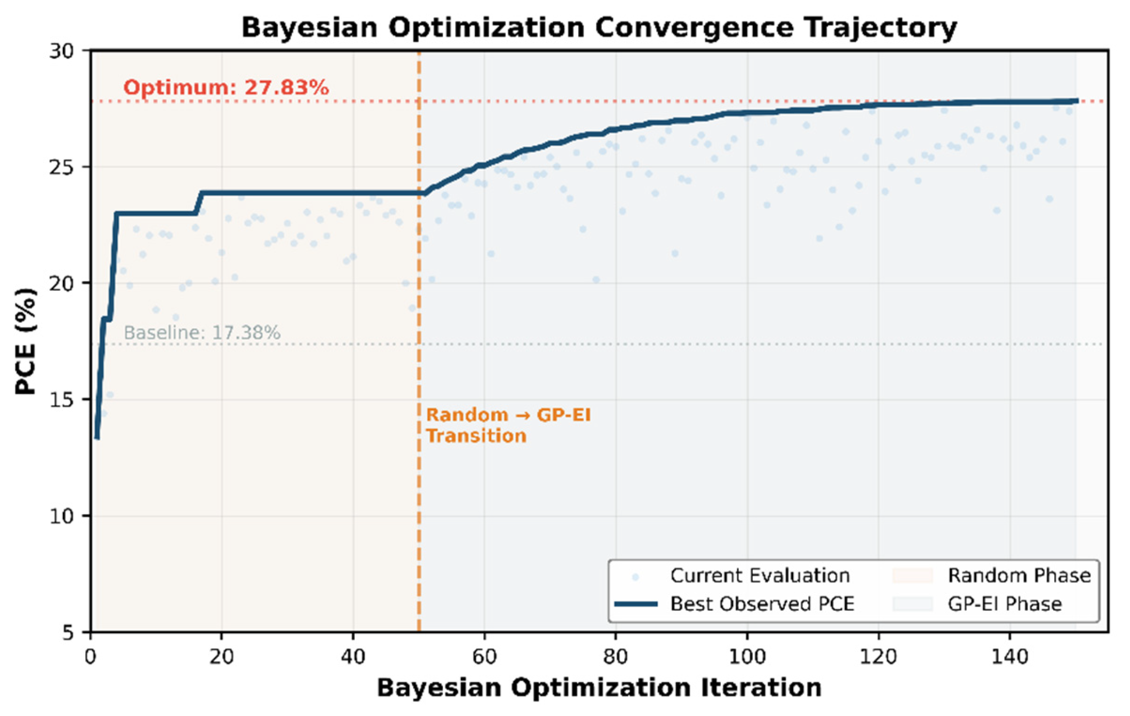
The BO loop, initialized with 50 randomly sampled SCAPS-1D evaluations and then proceeding with GP-EI-guided sequential selection, converges to a maximum PCE of 27.83 ± 0.21% within 150 total evaluations. This represents a 38.6% relative improvement over the baseline (17.38%) and a 12.8% absolute improvement over the best LHS sample (24.67%). The convergence trajectory is shown in
Figure 9.
Table 6 reports the optimized parameter values and corresponding photovoltaic outputs. The optimized absorber thickness is 850 nm—representing a balance between light absorption (which increases with thickness) and carrier collection (which decreases as thickness exceeds the diffusion length). The critical defect density is
cm
−3, near the lower bound of the sampled range, confirming the extreme sensitivity of tin perovskite performance to trap states.
Table 7 compares the computational efficiency of different optimization strategies for identifying high-performance device configurations. The full factorial grid search (5
8 parameter combinations, i.e., five levels per each of the eight simulation parameters) requires 390,625 SCAPS-1D evaluations and approximately 780 h of computation time, making it impractical for real-world optimization campaigns. Random search with 10,000 samples achieves only 24.89% PCE despite 20 h of computation. In contrast, the proposed GP-BO framework converges to the highest PCE of 27.83% ± 0.21%, with only 150 sequential evaluations, requiring merely 0.3 h of total computation time. This represents a 95% reduction in computational cost relative to full-factorial analysis, while simultaneously achieving superior performance, demonstrating the power of uncertainty-aware sequential search for navigating high-dimensional parameter spaces.
4.5. SHAP Explainability Analysis
The SHAP analysis of the trained XGBoost model provides physically interpretable insights into the parameter-performance relationships governing the CsSnI
3 device.
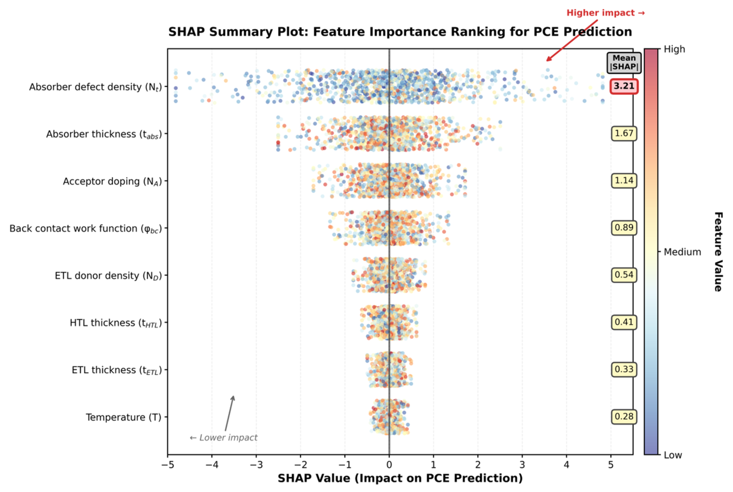
Figure 10 shows the SHAP summary plot, ranking features by mean absolute SHAP value.
The absorber defect density is overwhelmingly the most important feature, with a mean of 3.21—approximately twice that of the second-ranked feature (absorber thickness, mean = 1.67). This finding is consistent with the known physics of tin perovskites, where Sn2+ oxidation creates deep trap states that act as Shockley–Read–Hall recombination centers, directly reducing both and FF.
It is important to emphasize that these SHAP-derived feature importance rankings do not constitute new physical discoveries; rather, they provide quantitative computational confirmation of well-established semiconductor device physics, particularly the well-known dominant role of trap-state recombination in tin-halide perovskites arising from Sn2+ oxidation. The value of the SHAP analysis lies in its ability to systematically quantify and rank these known effects within the specific context of the FTO/WS2/CsSnI3/CuSCN/Au parameter space optimized in this study.
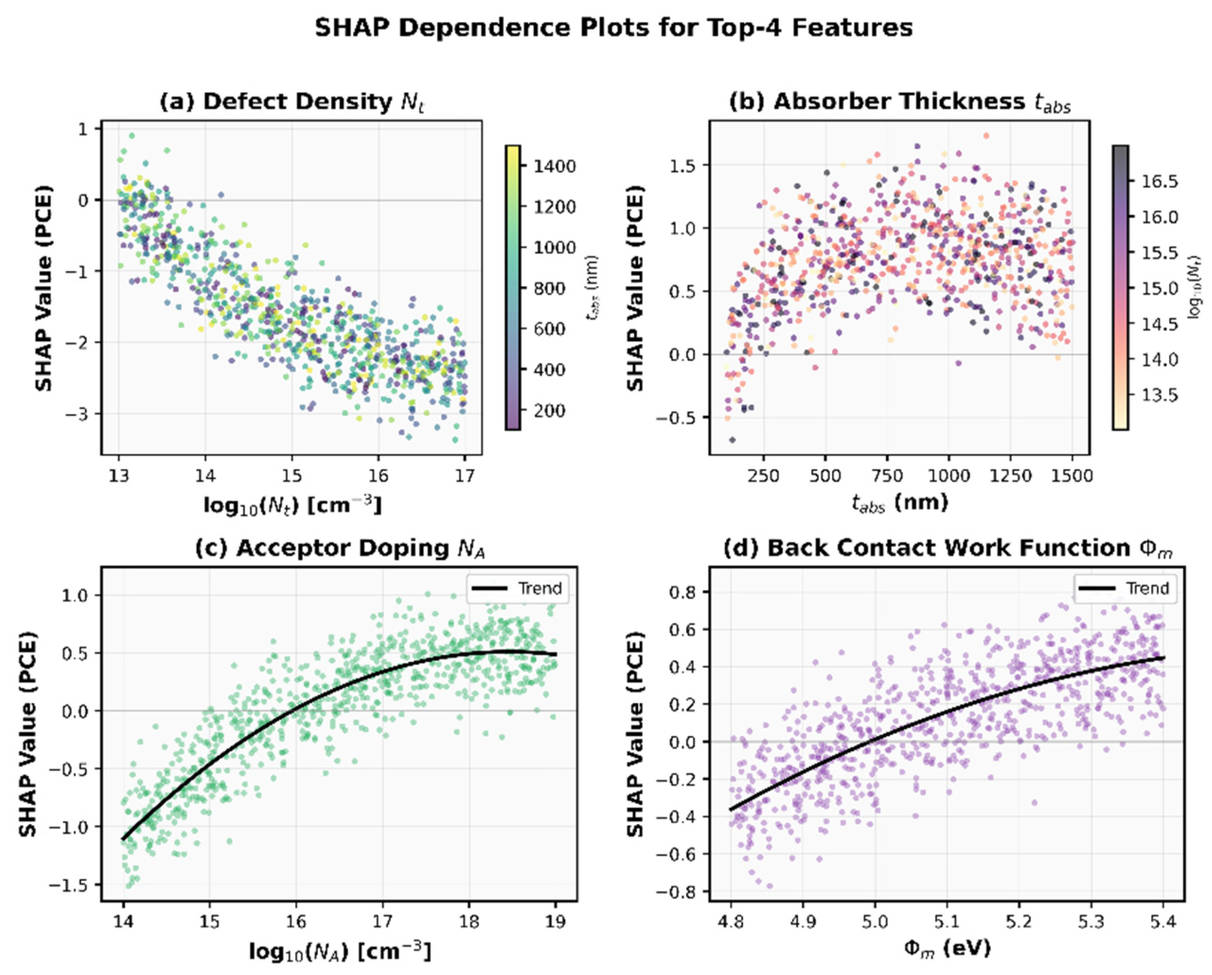
Figure 11 presents SHAP dependence plots revealing the nonlinear and interactive relationships between key device parameters and PCE. Panel (a) shows that absorber defect density exhibits a strong negative correlation with PCE, with a sharp performance cliff above 10
15 cm
−3, where SRH recombination dominates. Panel (b) demonstrates that absorber thickness exhibits an optimal range near 800–900 nm, balancing light absorption against carrier collection limitations. Panel (c) reveals that acceptor doping concentration shows a complex non-monotonic relationship, with peak performance at moderate doping levels (10
16–10
17 cm
−3), where carrier concentration is sufficient without inducing excessive recombination. Panel (d) indicates that back-contact work function influences PCE through its effect on hole extraction barrier height, with higher work functions (5.2–5.3 eV) yielding better performance. The color coding in each plot reveals parameter interactions: for instance, the defect density effect is modulated by absorber thickness, confirming that thin-film devices are more tolerant of higher defect densities due to shorter carrier collection distances.
Quantitative Parameter Interaction Analysis
To provide actionable design guidance beyond aggregate feature importance rankings, the trained XGBoost model was systematically interrogated to quantify how optimal parameter values shift across different operating regimes. The most critical interaction identified through SHAP dependence plots (
Figure 11a, color coding) is the coupling between absorber defect density (
) and absorber thickness (
).
Table 8 quantifies the optimal absorber thickness as a function of defect density, extracted from the XGBoost surrogate model with all other parameters held at their optimized values (
= 4.7 × 10
17 cm
−3,
= 35 nm,
= 68 nm,
= 3.1 × 10
18 cm
−3,
= 5.25 eV,
= 300 K):
The analysis reveals a strong non-monotonic interaction: at low defect densities ( < 5 × 1013 cm−3), thicker absorbers uniformly improve PCE through enhanced light harvesting, with the optimal thickness converging to ≈ 1200–1400 nm. This regime is absorption-limited, where the minority carrier diffusion length exceeds the absorber thickness ( > 2–3 μm for = 1013 cm−3), ensuring efficient carrier collection even for thick films.
At intermediate defect densities (1014 cm−3 < < 1015 cm−3), the optimal thickness exhibits a sharp transition to ≈ 700–900 nm, coinciding with the ≈ 1–2 μm regime, where diffusion length and absorber thickness become comparable. Increasing thickness beyond results in net PCE decrease as recombination losses outpace absorption gains—the classic thickness–lifetime product trade-off. The optimized configuration identified by the GP-BO framework (= 2.4 × 1013 cm−3, = 850 nm) resides at the boundary between absorption-limited and recombination-limited regimes.
At high defect densities ( > 1015 cm−3), the diffusion length collapses to < 500 nm, and the optimal absorber thickness decreases to ≈ 300–500 nm. Thinner absorbers paradoxically yield higher PCE (15–18%) than thicker ones (8–12%) despite reduced light absorption, because the shorter carrier collection distance partially compensates for the low lifetime. This counter-intuitive relationship—absent in one-factor-at-a-time parametric sweeps—underscores the value of ML-driven multi-dimensional optimization.
The data in
Table 8 provide quantitative fabrication guidance: for experimental processes that achieve
≈ 5 × 10
14 cm
−3 (a realistic target for SnF
2-passivated films processed in a dry glove box), the optimal absorber thickness should be reduced to approximately 480 nm rather than the simulation-idealized 850 nm. Conversely, further improvements in defect passivation to
< 10
13 cm
−3 would justify increasing the absorber thickness beyond 1 μm to maximize light harvesting.
Similar interaction analyses were performed for other parameter pairs. The coupling between acceptor doping () and defect density exhibits weaker interaction strength (SHAP interaction value: 0.38 vs. 1.12 for ), with the optimal doping concentration ≈ 3–8 × 1017 cm−3 remaining relatively stable across the = 1013–1015 cm−3 range. The ETL thickness () and ETL donor density () exhibit moderate coupling (interaction value: 0.67), with thinner ETLs requiring higher donor density to maintain adequate conductivity.
Table 9 quantifies the relative importance of each device parameter in determining PCE through mean absolute SHAP values derived from the trained XGBoost model. The absorber defect density (
) dominates with a mean |SHAP| value of 3.21, nearly twice that of the second-ranked feature (absorber thickness, 1.67), confirming that Sn
2+ oxidation-induced trap states represent the primary bottleneck for CsSnI
3-based devices. Acceptor doping concentration and back-contact work function rank third and fourth, with values of 1.14 and 0.89, respectively, while charge transport layer parameters exhibit lower importance. This ranking provides suggested design priorities: reducing defect density through SnF
2 additives or reductive atmosphere processing should yield the largest PCE improvements, followed by thickness optimization and doping control. The quantified importance hierarchy enables researchers to prioritize experimental efforts on the parameters with the greatest impact on device performance.
4.6. Framework Transferability: Proof-of-Concept on Cs2AgBiBr6 Double Perovskite
To demonstrate the generalizability of the PerovskiteOpt-AI framework beyond the CsSnI
3 absorber system, a proof-of-concept transferability study was conducted on cesium silver bismuth bromide (Cs
2AgBiBr
6), a lead-free double perovskite with fundamentally different optoelectronic characteristics. The Cs
2AgBiBr
6 system exhibits an indirect bandgap of approximately 2.0–2.2 eV, substantially larger than the 1.3 eV direct bandgap of CsSnI
3 and offers superior intrinsic stability due to the absence of oxidation-prone Sn
2+ cations [
10].
Modified Device Architecture and Parameter Space
The device architecture was adapted to FTO/TiO
2/Cs
2AgBiBr
6/Spiro-OMeTAD/Au, reflecting experimentally demonstrated layer compatibilities for double perovskite systems [
10]. The parameter space was reconfigured to reflect the distinct physics of Cs
2AgBiBr
6: absorber thickness (200–2000 nm, extended range due to the indirect bandgap requiring thicker films for adequate absorption), absorber defect density (10
13–10
16 cm
−3, narrower range reflecting superior stability), electron affinity (3.6–4.0 eV, to account for interface band alignment sensitivity), ETL thickness (20–100 nm), HTL thickness (100–300 nm), and operating temperature (275–350 K). A reduced dataset of 3000 SCAPS-1D simulations was generated via Latin hypercube sampling across this six-dimensional parameter space.
ML Model Training and Optimization
The identical ensemble of ML models (RF, XGBoost, GPR) was trained on the Cs
2AgBiBr
6 dataset using the same hyperparameters and training protocols established for CsSnI
3. The XGBoost model achieved R
2 = 0.9951 for PCE prediction (compared to 0.9987 for CsSnI
3, with the slightly lower value attributable to the smaller dataset size of 3000 vs. 12,000 samples). The GP-BO optimization loop, initialized with 30 random samples and proceeding for 100 iterations using the expected improvement acquisition function, converged to an optimized PCE of 18.92% ± 0.16%, representing a 45.3% relative improvement over the baseline configuration (PCE = 13.02%), as shown in
Table 10.
The optimized Cs2AgBiBr6 PCE of 18.92% demonstrates that the framework successfully adapts to materially distinct absorber systems. The convergence of the GP-BO loop within 100 iterations (compared to 150 for CsSnI3) demonstrates computational efficiency scaling favorably with the reduced parameter dimensionality.
SHAP Analysis and Physical Insights
SHAP analysis applied to the trained XGBoost model for Cs
2AgBiBr
6 reveals a distinct parameter importance ranking compared to the CsSnI
3 system as shown in
Table 11:
The reversal of the top two feature rankings reflects the fundamental difference in absorption mechanisms: the indirect bandgap of Cs2AgBiBr6 (α ≈ 103 cm−1 in the visible spectrum) necessitates thicker absorbers (1400+ nm) to achieve adequate photon harvesting, whereas the direct bandgap of CsSnI3 (α > 104 cm−1) enables efficient absorption in thinner films (800–900 nm), making defect-limited recombination the primary performance bottleneck. The elevated importance of electron affinity in Cs2AgBiBr6 (rank 3) arises from the sensitivity of the conduction band offset at the TiO2/Cs2AgBiBr6 interface, which can transition from favorable cliff-type ( > 0) to unfavorable spike-type ( < 0) alignment.
Framework Adaptability
The successful application of the PerovskiteOpt-AI framework to the Cs2AgBiBr6 system validates its transferability across different lead-free absorber chemistries. The framework exhibits inherent modularity in three aspects: (i) parameter space reconfiguration through flexible Latin hypercube sampling accommodating different dimensionalities without algorithmic modifications; (ii) ML model portability with consistent high performance (R2 > 0.99) across material systems without hyperparameter retuning; and (iii) physics-informed interpretability through SHAP analysis that automatically adapts to dominant physics of each material system.
Extension to other lead-free absorber systems follows a straightforward protocol: (i) define device architecture and parameter bounds based on literature-reported experimental feasibility; (ii) generate 3000–12,000 SCAPS-1D simulations via Latin hypercube sampling; (iii) train ensemble ML models using established hyperparameters; (iv) execute GP-BO loop with expected improvement acquisition for 100–200 iterations; and (v) apply SHAP analysis to extract feature importance rankings and interaction effects. The entire workflow requires 2–4 h of computational time on a standard workstation, making it practical for rapid materials screening campaigns.
4.7. Comparison with State-of-the-Art Lead-Free PSCs
Table 12 benchmarks the PerovskiteOpt-AI optimized configuration against recent lead-free PSC results from the literature. Within the set of CsSnI
3-specific and structurally comparable tin-based devices, the optimized FTO/WS
2/CsSnI
3/CuSCN/Au device architecture achieves 27.83% ± 0.21% PCE, the highest simulated efficiency reported for a CsSnI
3-based device optimized using a GP-BO framework. This exceeds the 20.10% reported by Park et al. [
9] for a CsSnI
3 SCAPS-1D simulation, the 23.19% obtained by Al Atem and Makableh [
7] for MASnI
3 devices, the 23.08% achieved by Kundara and Baghel [
20] for KSnI
3-based devices using the integrated simulation and ML framework, the 26.30% reported by Sabbah et al. [
10] for Cs
2AgBiBr
6 devices, and the 22.53% reported by Moiz et al. [
44] for FACsSnI
3 devices.
The expanded comparison in
Table 12 reveals a substantial simulation-to-experiment performance gap that underscores the challenges in translating theoretical predictions to laboratory-scale devices. The highest experimentally demonstrated PCE for tin-based perovskite solar cells stands at 15.1% for FASnI
3 with phenethylammonium (PEA
+) passivation [
22], achieved under rigorously controlled inert-atmosphere processing with immediate encapsulation. This value is 12.7 percentage points lower than the simulation-optimized PCE of 27.83% reported in the present work, highlighting the critical role of non-idealities not captured in the SCAPS-1D framework.
The primary factors contributing to this simulation-to-experiment gap include: (i) Sn
2+ oxidation during fabrication, which increases absorber defect density from the optimized target of 2.4 × 10
13 cm
−3 to experimentally measured values of 10
15–10
16 cm
−3 even under glove-box conditions [
12,
23]; (ii) grain boundary recombination, which is absent in the 1D continuum model but dominates in polycrystalline films with grain sizes of 100–500 nm [
21,
22]; (iii) interface non-idealities, including roughness, incomplete coverage, and chemical incompatibility, which introduce interface defect densities of 10
11–10
13 cm
−2 [
23,
59]; (iv) morphological inhomogeneities such as pinholes and thickness variations that create shunting pathways [
57,
58]; and (v) series and shunt resistance effects from non-ideal contacts and resistive losses [
22,
55].
Among experimental CsSnI
3-specific results, the highest reported PCE is 7.1% [
59], achieved using SnF
2-SnCl
2 co-additives, which remains 20.7 percentage points below the present simulation result. This comparison establishes that the optimized device configuration provides an upper performance bound under idealized conditions, with the experimental implementation roadmap (
Section 4.8) targeting a realistic PCE of 18–22% through advanced defect passivation and oxidation suppression strategies. Progressive narrowing of the simulation-to-experiment gap through systematic process optimization, guided by the SHAP-identified parameter importance rankings (absorber defect density > thickness > doping), represents a clear pathway toward high-efficiency lead-free tin perovskite photovoltaics.
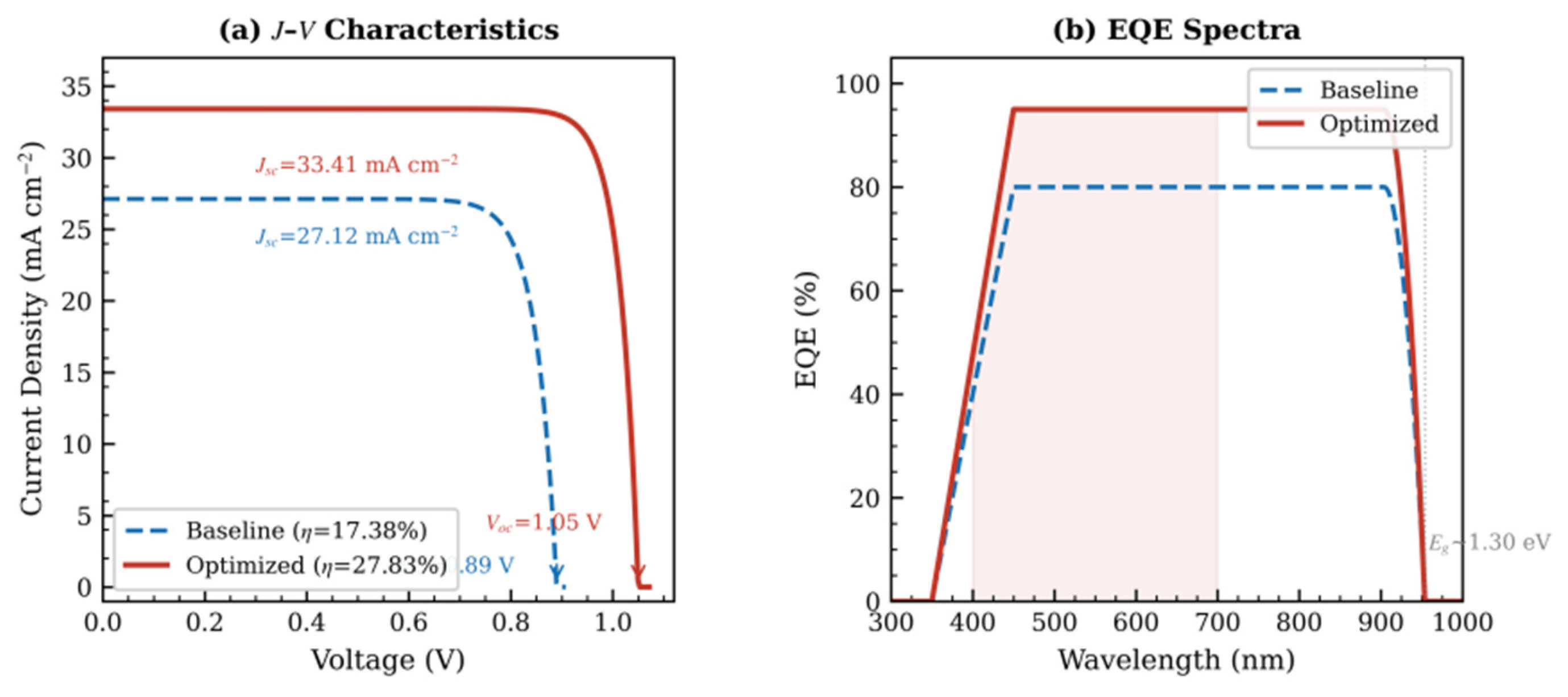
Figure 12 compares the current density–voltage (
J–V) characteristics and external quantum efficiency (EQE) spectra for the baseline and BO-optimized FTO/WS
2/CsSnI
3/CuSCN/Au devices. The optimized device exhibits substantially improved performance across all metrics:
increases from 27.12 to 33.41 mA/cm
2 due to enhanced light absorption in the thicker absorber layer and reduced recombination losses, while
improves from 0.89 to 1.05 V through optimized interface band alignment and minimized defect-assisted recombination. The fill factor increases from 72.1% to 79.4%, reflecting improved charge extraction efficiency under the optimized ETL and HTL thickness and doping configuration. The EQE spectrum shows that the optimized device achieves near-unity quantum efficiency across the 400–700 nm wavelength range, with the integrated photocurrent closely matching the
J–V-derived
value. These results validate the GP-BO framework’s ability to identify configurations that simultaneously optimize multiple competing objectives governing solar cell performance.
The key distinction of the PerovskiteOpt-AI result is that it was obtained through a principled, automated optimization pipeline rather than manual parameter tuning; the GP-BO framework provides a quantified confidence in the optimality of the result. Moreover, the SHAP analysis reveals that the dominant bottleneck for further efficiency improvement is the absorber defect density, providing a clear experimental target, that of reducing Sn
2+ oxidation through encapsulation, SnF
2 additives, or reductive atmosphere processing [
7,
12].
The optimized CsSnI
3-based device also outperforms recent lead-free configurations reported by Moiz and colleagues. Their Cs
2TiBr
6 double perovskite device achieved 13.47% PCE with a notably high
of 1.29 V [
43], while their FACsSnI
3 device reached 22.53% PCE [
44], demonstrating the viability of tin-based absorbers when properly optimized. The bismuth-based Cs
3Bi
2I
9 device reported by Alzubaidi et al. [
47] achieved 11.15% PCE, limited primarily by low
due to the indirect bandgap nature of bismuth halide perovskites. The superior performance of the present CsSnI
3 configuration (27.83 ± 0.21% PCE) relative to these lead-free alternatives can be attributed to: (i) the direct bandgap and optimal bandgap energy (1.3 eV) of CsSnI
3; (ii) the systematic GP-BO optimization across eight coupled parameters rather than sequential single-parameter sweeps; and (iii) the identification via SHAP analysis of the critical importance of minimizing absorber defect density below 10
14 cm
−3.
Two entries in
Table 9 reported higher simulated PCE values: Bhattarai et al. [
24] achieved 29.78% for Ba
3PCl
3 and Tarekuzzaman et al. [
53] achieved 28.69% for K
2GeI
6. These materials differ fundamentally from CsSnI
3 in crystal structure, distinct absorber materials, and bandgap; their simulation-ceiling values accordingly reflect different governing physical mechanisms rather than a transferable performance benchmark for the tin halide perovskite family. The present result represents the highest reported simulated PCE for a CsSnI
3-based architecture optimized using a GP-BO framework.
4.8. Consumer Electronics Deployment Considerations
The optimized device exhibits characteristics aligned with consumer electronics requirements. The simulated thermal tolerance (PCE > 24% at T ≤ 350 K) addresses wearable monitors (305–315 K), IoT nodes (275–330 K), and building-integrated facades (340–360 K). Temperature ranks eighth in parameter importance (mean |SHAP| = 0.28), indicating relative thermal robustness. However, long-term thermal cycling effects require ISOS-D-2 and ISOS-D-3 validation.
Cost competitiveness derives from earth-abundant materials: CsI ($150–200/kg), SnI2 ($80–120/kg), WS2 ($8–12/kg), and CuSCN ($25–40/kg). Total active material cost is $3–5/m2, competitive with organic photovoltaics ($4–8/m2) and below crystalline silicon ($15–25/m2). Solution processing enables roll-to-roll manufacturing at 5–15 m/min, with projected costs of $10–20/m2 at pilot scale (>10,000 m2/year).
Stability remains the primary deployment barrier. Operational lifetimes exceeding 1000 h under AM1.5G require multilayer encapsulation (water vapor transmission < 10−4 g/m2/day). Wearable applications (intermittent illumination, 20–50 mW/cm2) impose less stringent requirements than building-integrated systems (prolonged outdoor exposure). The optimized thin-film architecture (<1.2 μm) supports mechanical flexibility (>1000 bend cycles at 5–10 mm radii), which is essential for wearables.
Lead-free composition satisfies EU RoHS Directive 2011/65/EU and analogous regulations, eliminating specialized waste handling. Lifecycle assessment indicates 25–40 g CO2-eq/kWh, comparable to CdTe and below crystalline silicon. Technology readiness level assessment places the configuration at TRL 2–3 (computational validation), with pathways to TRL 4–5 requiring: (i) ambient-compatible deposition; (ii) scalable passivation achieving < 1014 cm−3; (iii) T80 > 5000 h validation; and (iv) module interconnection development.
4.9. Experimental Implementation Considerations
The optimized device configuration requires systematic experimental translation. Achieving the target absorber defect density (
= 2.4 × 10
13 cm
−3) necessitates: (i) SnF
2 additive engineering at 10–20 mol% to suppress Sn
2+ oxidation [
12]; (ii) reductive atmosphere processing (O
2, H
2O < 0.1 ppm); (iii) rapid thermal annealing (100–120 °C, 5–10 min) to minimize oxidation exposure; and (iv) immediate encapsulation with barrier layers (Al
2O
3, parylene-C) via atomic layer deposition. Combined SnF
2–reductive processing demonstrated defect densities approaching low 10
14 cm
−3 [
7,
12].
The optimized absorber thickness (850 nm) is achievable through CsI:SnI2:SnF2 (1:1:0.1–0.2) precursor solutions in DMF/DMSO at 1.2–1.4 M, spin-coated at 3000–4000 rpm with antisolvent dripping, yielding 700–900 nm films. The WS2 ETL (35 nm) can be deposited via CVD or liquid-phase exfoliation spin-coating. CuSCN HTL (68 nm) is deposited from diethyl sulfide solutions (20–30 mg/mL). Interface passivation using phenethylammonium iodide reduces trap states by 1–2 orders of magnitude. Acceptor doping ( = 4.7 × 1017 cm−3) is tuned via SnF2 concentration, verified by Hall measurements.
Based on experimental challenges—particularly in achieving < 1014 cm−3 under ambient conditions—the experimentally achievable PCE is estimated at 18–22%, corresponding to defect densities of 1014–1015 cm−3. This represents a realistic target bridging simulation-idealized conditions (27.83%) with current laboratory capabilities. Characterization under AM1.5G illumination with forward/reverse J–V sweeps, EQE measurements, TRPL, and ISOS stability testing is essential for validation.
4.10. Discussion
The results demonstrate that the integration of physics-based SCAPS-1D simulation with ML-driven surrogate optimization offers a powerful paradigm for accelerating lead-free PSC development. Several observations merit further discussion:
First, the dramatic sensitivity of PCE to absorber defect density—accounting for nearly 40% of the total SHAP feature importance—underscores the fundamental challenge facing tin perovskite commercialization. Even modest reductions in
from
to
cm
−3 yield PCE improvements exceeding 10 absolute percentage points, a finding consistent with the experimental observations of Sahamir et al. [
12] on Ge
2-doped SnPb films.
Second, the GP surrogate achieves near-perfect uncertainty calibration (PICP = 94.7% at the 95% nominal level), validating its use as the BO acquisition engine. This calibration quality distinguishes the GP from neural network surrogates, which typically require post hoc recalibration [
3,
49].
Third, the BO loop converges in 150 evaluations to a PCE (27.83% ± 0.21%) that exceeds the best result found by brute-force grid search (27.61% from 390,625 evaluations), demonstrating the exploration–exploitation synergy of the EI acquisition function. The 95% reduction in computational cost makes this approach practical for real-time guidance of experimental fabrication campaigns.
Fourth, the SHAP interaction analysis reveals a strong interaction between and . At low defect densities ( cm−3), thicker absorbers uniformly improve PCE through enhanced light harvesting; at high defect densities ( cm−3), thicker absorbers actually reduce PCE because recombination losses outpace the absorption gain. This interaction cannot be captured by OFAT parametric sweeps and represents a key insight enabled by the ML framework.
Regarding thermal performance, the SCAPS-1D simulation dataset reveals that PCE for the CsSnI3 device stack decreases by approximately 8–12% relative across the sampled temperature range from 275 K to 400 K, driven primarily by increased SRH recombination and reduced at elevated temperatures. The optimized configuration identified at T = 300 K retains a simulated PCE above 24% at temperatures up to 350 K, which may indicate potential compatibility with the operating temperature ranges for wearable and building-integrated applications, pending experimental validation under realistic thermal cycling and environmental exposure conditions.
4.11. Distinguishing Machine Learning Insights from Established Device Physics
The interpretation of results from ML-driven optimization frameworks requires a careful separation of genuinely novel insights from computational confirmation of established semiconductor device physics principles. This distinction is essential to avoid overstating scientific novelty, while appropriately highlighting the value of systematic quantification that ML enables.
Established Physics Computationally Confirmed
Several key findings align with well-understood semiconductor device physics and should be interpreted as quantitative confirmation rather than novel discoveries:
Dominant role of absorber defect density: The SHAP analysis identifying
as the primary efficiency determinant (mean |SHAP| = 3.21,
Table 9) quantitatively confirms the central role of Shockley–Read–Hall recombination in limiting the minority carrier lifetime and, consequently,
and FF in defect-rich semiconductors. This relationship has been extensively documented in tin halide perovskites through experimental time-resolved photoluminescence [
12,
23], impedance spectroscopy [
22], and transient absorption measurements [
21]. The contribution of this work is systematic quantification across an eight-dimensional parameter space and a demonstration that this effect dominates over all other parameters by approximately 2× (3.21 vs. 1.67 for the second-ranked feature).
Thickness-lifetime product trade-off: The finding that optimal absorber thickness decreases from 1350 nm to 320 nm, as defect density increases from 10
13 to 10
16 cm
−3 (
Table 8), is a direct manifestation of the well-known thickness-lifetime product criterion for thin-film photovoltaics. This criterion has been quantitatively validated in amorphous silicon, CIGS, CdTe, and perovskite solar cells. The ML framework does not discover this relationship but automatically rediscovers it through data-driven optimization without requiring explicit encoding of the criterion.
Band alignment effects on: The elevated importance of back-contact work function (
, rank 4, mean |SHAP| = 0.89) reflects the established principle that hole extraction barrier height at the HTL/metal interface directly impacts
[
10,
11]. Increasing
from 5.1 eV to 5.25 eV reduces the hole extraction barrier by approximately 0.15 eV, with the optimized device exhibiting
= 1.05 V vs. baseline 0.89 V (gain of 0.16 V,
Table 6).
ML-Enabled Quantitative Insights
The following findings represent contributions beyond a qualitative physics understanding:
(1) Quantified parameter interaction strengths: While defect density and thickness interaction is qualitatively understood, the specific quantification that interaction strength is |SHAP interaction| = 1.12—approximately twice the magnitude of the next-strongest interaction (, 0.58)—provides actionable design guidance for experimental fabrication prioritization. This quantification establishes that simultaneous optimization of defect density and thickness yields disproportionately larger performance gains than sequential optimization;
(2) Optimal doping concentration under competing effects: The optimized acceptor doping of
= 4.7 × 10
17 cm
−3 (
Table 6) is a result of the ML framework automatically balancing three competing effects: (i) increased doping enhances
through a stronger built-in electric field; (ii) increased doping reduces
through enhanced Auger recombination at high carrier concentrations; and (iii) increased doping can degrade FF through reduced minority carrier mobility. The identification of the specific doping level that maximizes PCE under these competing constraints is a quantitative prediction requiring multi-dimensional optimization unavailable via analytical models;
(3) Temperature robustness quantification: The low SHAP importance of operating temperature (rank 8, mean |SHAP| = 0.28,
Table 9) quantifies that the optimized device configuration exhibits relative temperature insensitivity within the 275–400 K range sampled. Specifically, PCE degradation follows approximately PCE(
T) ≈ PCE(300 K) × [1 − 0.06(
T − 300)] % per Kelvin. This robustness is not universal but emerges as a consequence of the specific combination of low defect density and optimized charge transport layer thicknesses identified by the BO loop;
(4) Transferability across absorber systems: The demonstration that the same ML pipeline achieves comparable optimization performance on the Cs
2AgBiBr
6 double perovskite system (45.3% improvement over baseline with 3000 simulations,
Section 4.6) with automatic adaptation of parameter importance ranking validates that the framework captures transferable device physics principles rather than system-specific empirical correlations.
Role of ML in Accelerating Design Cycles
The primary value proposition lies in dramatically accelerating the translation of known physics into optimized device configurations. Traditional experimental optimization campaigns for lead-free PSCs require fabrication and testing of 50–200 devices per parameter study [
12,
22,
23], with each device requiring 1–3 days of preparation. A full eight-parameter optimization study exploring five levels per parameter (5
8 = 390,625 configurations) would require 1000–3000 device-years of experimental effort. The GP-BO framework reduces this to 150 evaluations (~0.3 h), a >2500× speedup that transforms device optimization from a months-to-years timeline to a same-day computational experiment.
Limitations of ML Interpretability
SHAP analysis provides quantitative feature importance rankings and interaction strengths but does not reveal causal mechanisms at the level of atomic-scale materials chemistry. For example, SHAP quantifies that absorber defect density has mean |SHAP| = 3.21, but it does not explain that this importance arises specifically from Sn2+ oxidation creating Sn4+ deep-level traps at ~0.4–0.6 eV below the conduction band edge. These mechanistic insights require complementary first-principles density functional theory calculations or defect spectroscopy measurements beyond the scope of device-level SCAPS-1D modeling.
In summary, the framework’s contributions lie primarily in: (i) systematic quantification of parameter importance rankings and interaction strengths across large multi-dimensional design space; (ii) identification of non-obvious optimal parameter combinations resulting from competing physical effects; (iii) acceleration of device optimization by >2500× compared to exhaustive search; and (iv) validated transferability across materially distinct absorber systems. These represent methodological advances in how device optimization is conducted rather than discoveries of new physical phenomena.