
Article

Excitonic Effects and Antiferromagnetism in the Doped-Biased AB-Stacked Bilayer Graphene

Institute of Low Temperature and Structure Research, Polish Academy of Sciences, ul. Okólna 2, 50-422 Wrocław, Poland
*
Author to whom correspondence should be addressed.
Crystals 2026, 16(2), 95; https://doi.org/10.3390/cryst16020095
Submission received: 12 December 2025 / Revised: 19 January 2026 / Accepted: 24 January 2026 / Published: 29 January 2026

Abstract

We consider the direct orbital effect of an external magnetic field on the motion of electrons in reciprocal space in AB-stacked bilayer graphene subjected to a perpendicular magnetic field and an external electric field. For this purpose, the Peierls substitution is implemented using the symmetric gauge for the vector potential, and the electronic dispersion is reconstructed. The Lorentz potential arising from the Lorentz force acting on the electrons is included in the calculations. The effective chemical potential method is employed to incorporate the effects of Hubbard on-site repulsion, the external electric field, and Landau quantization of the allowed electronic states in reciprocal space. Local canted antiferromagnetic states are discussed, and their coexistence with excitonic states is found.

1. Introduction

AB-stacked bilayer graphene (BLG) has attracted significant scientific interest due to its extraordinary physical properties, which are mainly attributed to the opening of a sufficiently large and tunable band gap under the application of an external electric field [1,2,3,4,5,6,7,8,9,10,11,12].
The effect of a magnetic field on the electron hopping paths in graphene and graphene-based structures has been considered in many works [1,13] through the introduction of the Peierls phase [14,15,16,17]. In these studies, the electronic current operator and the resulting polarization correlation functions were calculated [18,19,20], typically without taking into account magnetic-field-induced modifications of the noninteracting electron dispersion relation.
Strong magnetic field effects [13], antiferromagnetic ordering [21,22], and various emergent phases—such as superconductivity [23], spin-wave excitations [24], excitonic states [25,26], and magnon modes [27,28]—have also been discussed in the context of AB-stacked bilayer graphene.
In monolayer graphene, the well-known quasiparticle energies exhibit a square-root dependence on both the Landau level index and the magnetic field in the low-wave-vector limit, as described by the linear Dirac Hamiltonian [29]. In contrast, for Bernal-stacked bilayer graphene, a linear dependence of the energy on the magnetic field has been obtained. Nevertheless, a complete understanding of this dependence in the full-wavelength regime is still lacking in the literature. In Ref. [30], the authors derived the high-energy spectrum of multilayer graphene by expanding the dispersion relation up to the third order in the wave vector around the Dirac point. By including the effects of trigonal warping, they found a B 3 / 2 dependence of the energy on the magnetic field as a third-order correction.
Recently, the authors of Ref. [31] calculated the internal voltage drop across a sheared AB-stacked bilayer graphene interface as a function of the applied tip voltage and determined the intrinsic dielectric properties of the AB BLG interface. The method employed accounts for the capacitive forces that govern the scaling of the potential drop across the sheared interface.
In this paper, we investigate the direct influence of an external magnetic field on the electron dispersion relation in reciprocal space in graphene layers, using the symmetric gauge for the magnetic field. In addition to the externally applied electric field, we introduce induced field potentials in the graphene layers by invoking the Lorentz-potential hypothesis. We then derive the effective layer potentials as functions of the applied external voltage, and our results are in good agreement with those reported in Ref. [31].
We consider both interlayer excitonic formation and a local antiferromagnetic order parameter. The canted antiferromagnetic regime [32] is adopted to describe the local antiferromagnetic order in the system. We analyze the voltage dependence of several physical parameters in AB-stacked bilayer graphene for different doping regimes. We find that the energy scales associated with the antiferromagnetic order parameter are significantly larger than those of the excitonic order. This result is opposite to what was reported for the same system in the absence of a magnetic field [32]. We attribute this behavior to the orbital effects of the magnetic field considered here.
The paper is organized as follows. Section 2 introduces the Hamiltonian in the presence of external fields and presents the theoretical framework. Section 3 provides a comprehensive analysis of the numerical results. Section 4 summarizes the main conclusions. Finally, Appendix A contains the analytical expressions for several important coefficients.

2. The Model

2.1. Hamiltonian of the System

We consider an AB-stacked bilayer graphene (BLG) system in the presence of an externally applied gate potential and a perpendicular magnetic field. Each honeycomb layer consists of two inequivalent sublattice sites, A and B, in the bottom layer ( = 1 ) and A ˜ and B ˜ in the top layer ( = 2 ). The layers are stacked in a way that the top atoms at the site positions B ˜ lie on top of the atoms in the bottom layer at the site positions A.

Peierls’s Substitution and the Linearized Fermionic Action

Semi-classically, when the electrons are exposed to the influence of the external magnetic field then the corresponding operators get extra phase modification. Let, a ^ ( a ^ ), b ^ ( b ^ ), a ˜ ^ ( a ˜ ^ ) and b ˜ ( b ˜ ^ ) refer to the fermionic annihilation (creation) operators at the atomic sites A, B, A ˜ and B ˜ , respectively. Then we can write the following transformations in the presence of the magnetic field: η ^ η ^ e i S r , where η are the fermionic sublattice variables η = a , b , a ˜ , b ˜ and S r is the semiclassical path S r = 0 r p + e c A d r , where A is the vector potential of the magnetic field. Then, for example, the product of two fermionic operators a ^ σ r b ^ σ r (where σ is the spin-variable) at the nearest neighbor lattice sites will be transformed in the following form
a ^ σ r b ^ σ r a ^ σ r b ^ σ r e i S r e i S r = a ^ σ r b ^ σ r e i r 0 p + e c A d r e i 0 r p + e c A d r = a ^ σ r b ^ σ r e i r r p + e c A d r = 1 n 0 a ^ 1 σ r b ^ 1 σ r e i r r e c A d r ,
where we have used the Bohr–Sommerfeld quantization rule for the free electronic orbits: r r p d r = 1 2 p d r = π n 0 , where n 0 is the principal orbital quantum number. In our case of graphene, we have n 0 = 2 and the Peierls phase is e i r r e c A d r . The model Hamiltonian of our AB system could be written as
H ^ 0 = γ 0 r r , σ a ^ σ r b ^ σ r e i r r d r p + e c A r + h . c . γ 0 r r , σ a ˜ ^ σ r b ˜ ^ σ r e i r r d r p + e c A r + h . c . t r , σ b ^ σ r a ˜ ^ σ r + h . c . μ r , η = a , b a ˜ , b ˜ n ^ η r ,
and the interaction part is
H ^ int = U η = a , b a ˜ , b ˜ r n ^ η r n ^ η r   + + W r σ σ n ^ b σ r n ^ a ˜ σ r + V act 2 r n ^ a ˜ r + V act 1 r n ^ b r .
First and second terms in Equation (2) describe the intra-layer hopping between the adjacent lattice sites r and r within the same layer and the hopping energy γ 0 is γ 0 2.8 eV [1] in graphene layers. In our calculations, we will use the parameter γ 0 as the unit of energy, i.e., γ 0 1 . The third term represents the inter-layer hopping between adjacent layers, described by the hopping energy t . Then the last term represents the chemical potential ( μ ) coupling with the electron densities at the individual atomic site positions and the electron density operators n ^ η r are defined as
n ^ η r = σ η ^ σ r η ^ σ r ,
Density operators in Equation (4) provide insight into the particle occupancy of the different sublattice sites.
The first term in the interaction Hamiltonian in Equation (3) represents the intra-layer Hubbard interaction with coupling strength U, accounting for electron–electron interactions on the same lattice site. The inter-layer Coulomb interaction between the electrons on the lattice sites B (in the layer = 1 ) and A ˜ (in the layer = 2 ) is modeled in the second term in Equation (3) with the repulsive interaction parameter W. The last two terms in Equation (3) show the coupling of the system with the external potential V applied to the system. Indeed, the potentials V act (with = 1 , 2 ), in Equation (3), describe the acting potentials in the layers coupled to the density terms in the layers. They are defined with the help of the external potential V and the induced potential V ind coming from the Lorentz potential of the magnetic field.
Indeed we hypothesize the existence of an electric field E in such a way that the Lorentz force is equal to the force created by this hypothetic electric field. Then, the electric field potential induced in the layers will be: V ind = ϵ g L | E | , where ϵ g is the dielectric constant in the graphene layers, L is the layer’s diagonal size, and | E | = E x 2 + E x 2 , because E = i E x + j E y . For the components of the electric field E x and E y we have E x = p y B / m c and E y = p x B / m c . Then, we take into account the in-plane energy Landau quantization, induced by the magnetic field: 2 k x 2 + k y 2 / 2 m ω B n + 1 2 , where ω B is the cyclotron frequency for the electrons: ω B = e B / m c . Thus, for V ind we get the following expression: V ind = 2 L ϵ g B μ B ω B c e n + 1 2 . The total electric field potentials in the layers will be
V act = 1 V 2 2 L ϵ g B μ B ω B c e n + 1 2 ,
where ϵ g is the dielectric constant of graphene layers (usually, the calculated value is ϵ g = 9.32 [31,33]), L is the macroscopic size of the individual graphene sheet (we set here L = L x 2 + L y 2 with L x = L y = 10 cm), μ B is the Bohr magneton, ω B = e B / m c is the cyclotron frequency, and n is the discrete quantum number of quantized electronic orbits in the presence of the perpendicular magnetic field (so-called Landau levels). In this paper, we set = 1 and μ B = 1 . The first and second terms in Equation (3) can be rewritten in a more convenient form to facilitate furthermore the linearization of the action. Specifically, for the U term, we have:
U r , η n ^ η r n ^ η r = U 4 n ^ η 2 r p ^ z η 2 r ,
where the operator p ^ z η r is the electron density polarization operator defined as:
p ^ z η r = n ^ η r n ^ η r .
In fact, the quantity p ^ z η r in Equation (7) is the spin polarization corresponding to difference in electron occupancy with the spin-up and spin-down states at the arbitrary site r . Next, passing to Grassmann variables [34] for the electrons the W interaction term in Equation (3) can be expressed as:
W r σ σ n b σ r n a ˜ σ r = W r , σ σ | ζ σ σ r | 2 ,
where the excitonic variables ζ σ σ r , and their complex conjugates ζ ¯ σ σ r are defined as:
ζ σ σ r = a ˜ ¯ σ r b σ r , ζ ¯ σ σ r = b ¯ σ r a ˜ σ r ,
Total fermionic action of the system is defined as:
S = S B + 0 β d τ H 0 τ + H int τ ,
where H 0 and H int are the Hamiltonians after passing to the Grassmann complex variables from the electronic operators in Equations (2) and (3), and S B , in Equation (10) is the fermionic Berry action in the system
S B = 0 β d τ r , η = a , b a ˜ , b ˜ η ¯ r τ τ η r τ .
Then, we can write the partition function of the system as
Z = η = a , b a ˜ , b ˜ D η ¯ D η e S .
We apply the Hubbard-Stratonovich decoupling to linearize the biquadratic fermionic density terms in Equations (6) and (8). The contributions to the fermionic action from the decoupling of the U term in Equation (6), are
S U = U 2 0 β d τ r η n η r τ n η r τ , S Δ p = U 2 0 β d τ r η p z η r τ p z η r τ .
The contribution arising from the decoupling of the inter-layer interaction term in Equation (8) is
S Δ = 0 β d τ r σ Δ σ σ a ζ ¯ σ σ a r τ + c . c . .
The parameter Δ σ σ , in the expression in Equation (14) and its complex conjugate Δ ¯ σ σ represents the excitonic order parameter, defined as:
Δ σ σ = W ζ σ σ r τ , Δ ¯ σ σ = W ζ ¯ σ σ r τ ,
Parenthesis , in Equations (13) and (15) are thermodynamic averages defined with the help of the partition function in Equation (12). We have
= 1 Z η = a , b a ˜ , b ˜ D η ¯ D η e S ,
where S in Equation (16) is the fermionic action after all decoupling contributions (obtained in Equations (13) and (14)):
S = S B + S U + S Δ p + S Δ + S V + 0 β d τ H 0 τ ,
where
S V = 0 β d τ r V 2 2 n a ˜ r τ + V 1 2 n b r , τ ,
As a simplification, we assume the homogeneous distribution of the excitonic gap parameter across the system and we suppose that the gap parameter is real. Therefore, we write:
Δ σ σ = Δ ¯ σ σ .
Index σ represents the spins of the particles involved in the pairing, as is customary. In our case, σ can take the values ↑ or ↓. Additionally, as it is mentioned above, we introduce the canted antiferromagnetic (AFM) order in the AB BLG system and we define the antiferromagnetic order parameter as
Δ AFM η = U 2 p z η r τ .
For the canted antiferromagnetic case, we expect that the antiferromagnetic order parameter alternates in sign across the layers and sublattices, which can be represented as:
Δ AFM b = Δ AFM a = Δ AFM b ˜ = Δ AFM a ˜ Δ AFM .
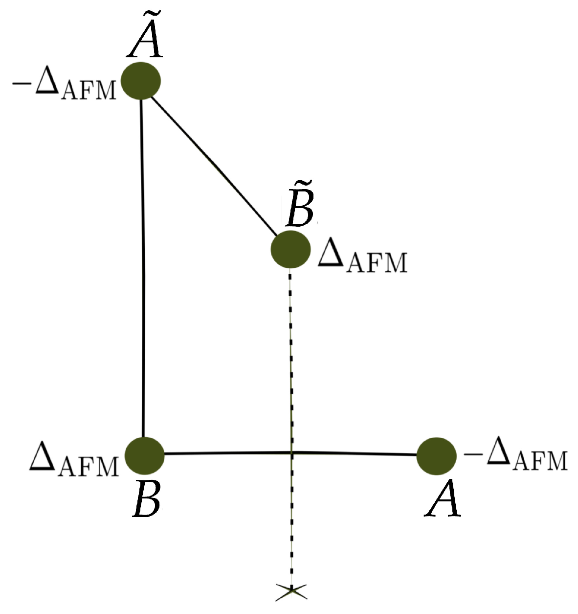
This staggered antiferromagnetic configuration is illustrated in Figure 1 and is called as the G-type antiferromagnetic ordering [32]. The ordering pattern in Equation (21) contributes to the electronic and magnetic characteristics of the AB-stacked BLG.
Having the fermionic action in the form presented in Equation (17), we can find the interplay between electronic correlations, magnetic order, and excitonic phenomena in the AB-stacked bilayer graphene system.

2.2. The Energy Spectrum

Here, we derive the energy spectrum of the AB bilayer graphene under consideration. For this we pass into the Fourier space representation of the fermionic Grassmann variables η σ r τ = 1 β N k ν n η σ k , ν n e i k r ν n τ , where ν n are the fermionic Matsubara frequencies ν n = π k B T ( 2 n + 1 ) / with n being integers and T the temperature.Then we write the obtained fermionic action in the Fourier space
S = 1 β N k ν n a ¯ k ν n a k ν n x μ + V ind V 2 + Δ AFM + U 4 1 κ δ n ¯ + b ¯ k ν n b k ν n x μ + V ind V 2 Δ AFM + U 4 1 κ δ n ¯ + a ˜ ¯ k ν n a ˜ k ν n x μ + V ind + V 2 + Δ AFM + U 4 1 κ + δ n ¯ + b ˜ ¯ k ν n b ˜ k ν n x μ + V ind + V 2 Δ AFM + U 4 1 κ + δ n ¯ + a ¯ k ν n a k ν n x μ + V ind V 2 Δ AFM + U 4 1 κ δ n ¯ + b ¯ k ν n b k ν n x μ + V ind V 2 + Δ AFM + U 4 1 κ δ n ¯ + a ˜ ¯ k ν n a ˜ k ν n x μ + V ind + V 2 Δ AFM + U 4 1 κ + δ n ¯ + b ˜ ¯ k ν n b ˜ k ν n x μ + V ind + V 2 + Δ AFM + U 4 1 κ + δ n ¯ + 1 β N k ν n γ k , B a ¯ σ k ν n b σ k ν n γ k , B b ˜ ¯ σ k ν n a ˜ σ k ν n + c . c . t + Δ β N k ν n b ¯ k ν n a ˜ k ν n c . c . t + Δ ¯ β N k ν n b ¯ k ν n a ˜ k ν n c . c . .
Here, x = i ν n and γ k , B is the dispersion in the reciprocal k space, which is obtained for the symmetric gauge of the vector potential of the external magnetic field. We have
γ k , B = γ 0 e i a 0 k x π B a 0 Φ 0 + + 2 e i a 0 2 k x π B a 0 Φ 0 cos a 0 3 2 k y + π B a 0 Φ 0 ,
where Φ 0 is the magnetic flux quantum Φ 0 = h c / e . Here, the symmetric gauge was used for the vector potential of the magnetic field A = B a 0 / 2 , B a 0 / 2 and a 0 is the lattice constant in graphene. We put throughout paper a 0 1 . We introduced in Equation (22) the inverse filling coefficient for the total average electron densities at the sites b 1 and a 2 and the average electron density difference function δ n ¯ between those sites
n ¯ a 2 + n ¯ b 1 = 1 κ , n ¯ a 2 n ¯ b 1 = δ n ¯ .
For the half-filling we have κ = 0.5 , which represents the situation where the maximum allowable number of electrons at each atomic site is 1. Hence, κ min = 0.25 which corresponds to full filling when each atomic site is occupied with 2 electrons. The values κ < κ min are excluded due to the violation of Pauli exclusion principle. Conversely, when κ > 0.25 , this indicates a doped bilayer case, and we can define the doping in the system as: x = 1 κ min 1 κ . For instance, if κ 0.25 , 1.0 , the electron doping x would then lie in the range x 0 , 3.0 . The action of the system can be expressed using the inverse Green’s function matrix G k σ 1 ν n , defined for each spin direction separately. For this, we introduce Gorkov spinor Ψ σ k , ν n and its complex conjugate Ψ ¯ σ k , ν n , pertinent to our analysis:
Ψ σ k , ν n = a σ k , ν n b σ k , ν n a ˜ σ k , ν n b ˜ σ k , ν n .
and the complex conjugate one
Ψ ¯ σ k , ν n = a ¯ σ k , ν n , b ¯ σ k , ν n , a ˜ ¯ σ k , ν n , b ˜ ¯ σ k , ν n .
Then the action of the system could be written as:
S Ψ ¯ , Ψ = 1 β N k ν n , σ Ψ ¯ σ k , ν n G σ 1 k , ν n Ψ σ k , ν n ,
where G σ 1 k , ν n is the inverse of the Green function matrix, defined for the given spin directions σ .

2.2.1. Inverse Green’s Function Matrix G 1 k , ν n

For the spin direction σ = , the inverse Green’s function matrix G 1 k , ν n is defined as:
G 1 k , ν n = x μ 1 eff + Δ AFM γ k , B 0 0 γ * k , B x μ 1 eff Δ AFM t Δ 0 0 t Δ ¯ x + μ 2 eff + Δ AFM γ * k , B 0 0 γ k , B x + μ 2 eff Δ AFM ,
where we have defined the effective chemical potentials μ 1 eff and μ 2 eff as
μ 1 eff = μ V act 1 U 4 1 κ δ n ¯ μ 2 eff = μ V act 2 U 4 1 κ + δ n ¯
and the energy spectrum for σ = configuration is
ϵ 1 k = 1 2 μ 1 eff μ 2 eff A k + 2 B k , ϵ 2 k = 1 2 μ 1 eff μ 2 eff + A k + 2 B k , ϵ 3 k = 1 2 μ 1 eff μ 2 eff A k 2 B k , ϵ 4 k = 1 2 μ 1 eff μ 2 eff + A k 2 B k ,
where
A k = 2 t 2 + 2 Δ AFM 2 + 2 | Δ | 2 + 4 | γ k , B | 2 + 2 t Δ + Δ ¯ + μ 1 eff μ 2 eff 2 , B k = 4 | γ k , B | 2 t 2 + | Δ | 2 + t Δ + Δ ¯ + μ 1 eff μ 2 eff 2 + t 2 + | Δ | 2 + t Δ + Δ ¯ + 2 Δ AFM μ 1 eff μ 2 eff 2 .

2.2.2. Inverse Green’s Function Matrix G 1 k , ν n

For the spin direction σ = , the inverse Green’s function matrix G 1 k , ν n is defined as:
G 1 k , ν n = x μ 1 eff Δ AFM γ k , B 0 0 γ * k , B x μ 1 eff + Δ AFM t Δ 0 0 t Δ ¯ x + μ 2 eff Δ AFM γ * k , B 0 0 γ k , B x + μ 2 eff + Δ AFM
and the energy spectrum for σ = configuration is
ϵ 1 k = 1 2 μ 1 eff μ 2 eff A k + 2 B k , ϵ 2 k = 1 2 μ 1 eff μ 2 eff + A k + 2 B k , ϵ 3 k = 1 2 μ 1 eff μ 2 eff A k 2 B k , ϵ 4 k = 1 2 μ 1 eff μ 2 eff + A k 2 B k ,
where
A k = A k , B k = 4 | γ k , B | 2 t 2 + | Δ | 2 + t Δ + Δ ¯ + μ 1 eff μ 2 eff 2 + t 2 + | Δ | 2 + t Δ + Δ ¯ 2 Δ AFM μ 1 eff μ 2 eff 2 .

2.2.3. Self-Consistent Equations

Here, we give the system of self-consistent equations for the chemical potential in the AB-BLG system, the average charge density difference between the lattice sites b and a ˜ , the excitonic order parameters Δ and Δ , and the antiferromagnetic order parameter in the system Δ AFM . They are defined in Equations (24), (15), and (20), respectively. We obtain
1 N k i = 1 4 α 1 i n F ϵ i + α 1 i n F ϵ i = 1 κ , 1 N k i = 1 4 α 2 i n F ϵ i + α 2 i n F ϵ i = δ n ¯ , W t + Δ 2 N k i = 1 4 α 3 i n F ϵ i = Δ , W t + Δ 2 N k i = 1 4 α 3 i n F ϵ i = Δ , U 8 N | k i = 1 4 α 4 i n F ϵ i α 4 i n F ϵ i | + | k i = 1 4 α 5 i n F ϵ i α 5 i n F ϵ i | + | k i = 1 4 α 6 i n F ϵ i α 6 i n F ϵ i | + + | k i = 1 4 α 7 i n F ϵ i α 7 i n F ϵ i | = Δ AFM .
Coefficients α i j σ (with i = 1 , , 7 ) in Equation (35) are given in Appendix A.

3. Results

In this Section, we present the numerical solution of the system of equations in Equation (35). The solutions have been done using the finite-difference approximation techniques [35] by employing the hybrid multi-root solver.
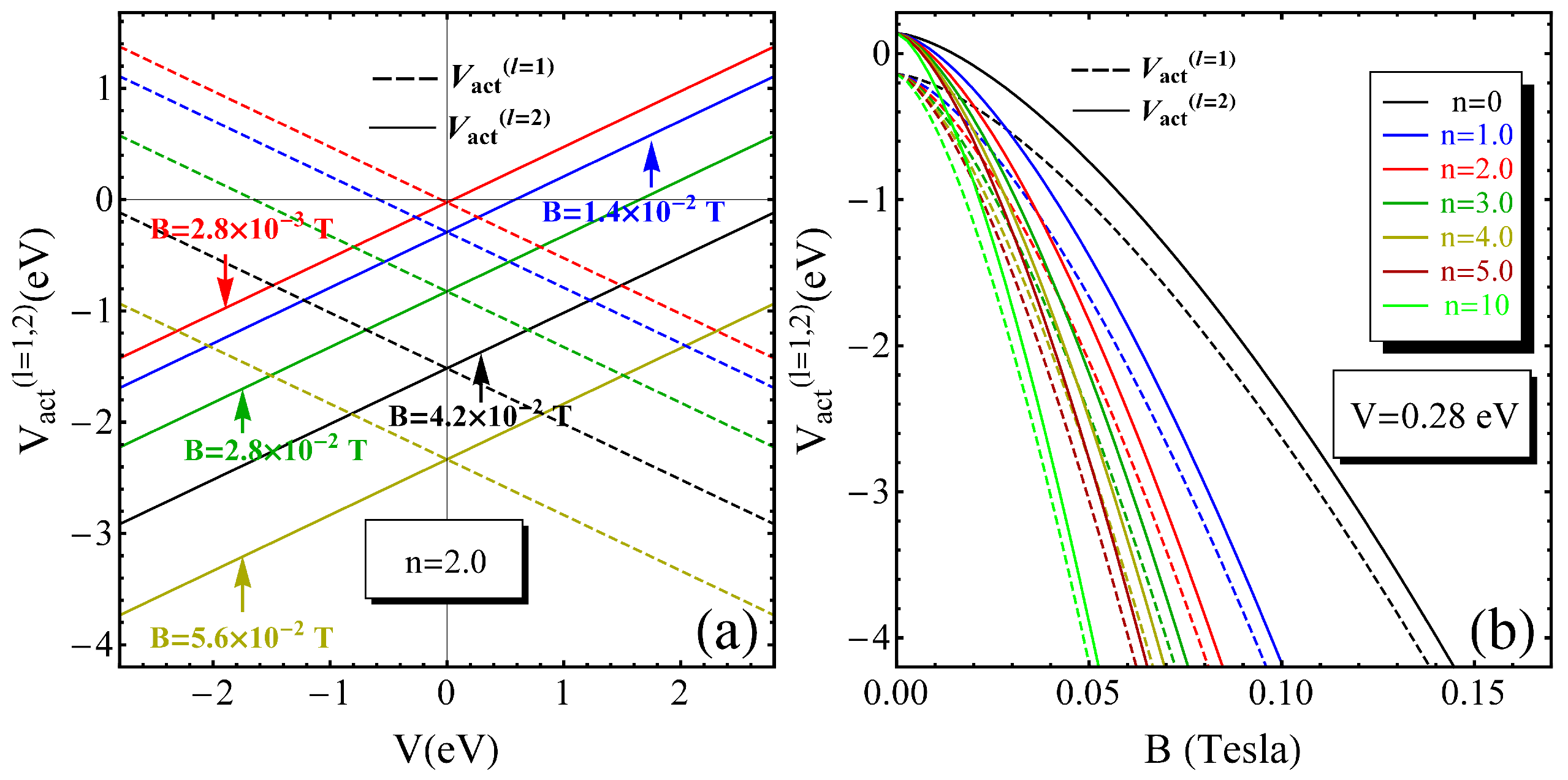
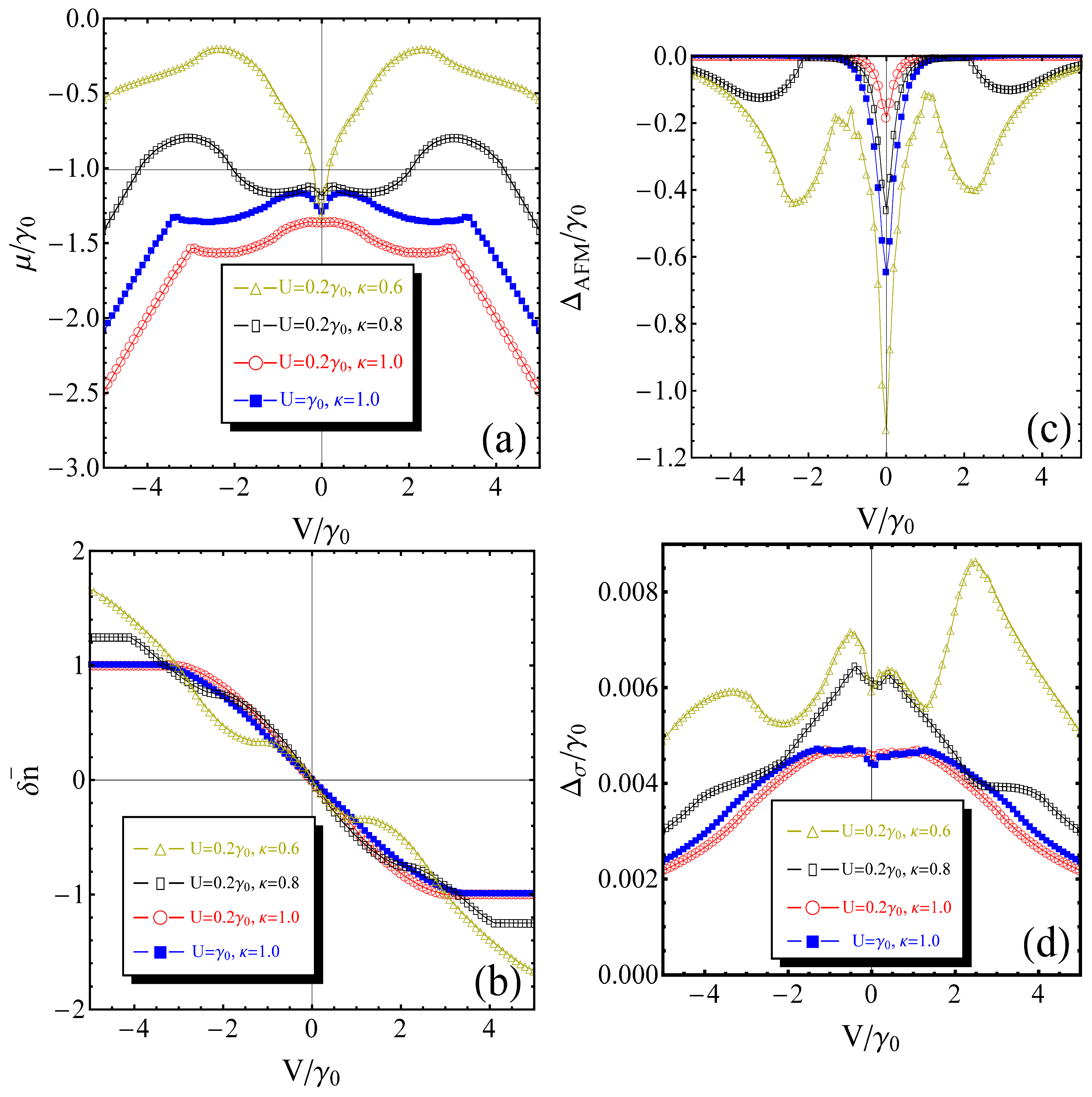
In Figure 2, we have shown the calculation results for the acting potentials in the layers, given by Equation (5). In Figure 2a, we considered the external field dependence of the acting potential, showing a constant voltage ratio V act = 2 / V = 0.5 . Different values of the external magnetic field have been employed, and the zero-temperature limit has been considered. We see that when increasing the magnetic field strength, the curves on the plane experiences parallel displacements. The similar dependence, with slightly lower value of voltage ratio, has been obtained in Ref. [31], where the authors considered the dielectric properties of AB stacked bilayer graphene without magnetic field effects. In Figure 2b, we have shown the magnetic field dependence of the acting electric field potentials in both layers with = 1 and = 2 for different values of the quantum numbers of electrons n. We observe that for the larger numbers n the action potentials decrease more rapidly with the magnetic field B, i.e., the outermost electrons on the quantized orbits in the reciprocal space modify more efficiently the intra-layer acting electric field potentials. In Figure 3, we have shown the numerical results for the calculated important physical parameters in the system as a function of the external gate potential V. The magnetic field is fixed at B = 0.0028 Tesla and the inter-layer Coulomb interaction is W = 0.2 γ 0 = 0.56 eV. In Figure 3a, we have shown the solution for the chemical potential, for different values of the intra-layer Coulomb interaction parameter U and for different values of the inverse filling coefficient κ . We see that for the large doping in the system: κ = 1 (see the red curve) and for the same value of the Hubbard-U interaction: U = 0.2 γ 0 = 0.56 eV the chemical potential is very high in absolute value, which makes the single-particle excitations in the system difficult and therefore the excitonic gap parameter, shown in Figure 3d, is small. The antiferromagnetic order parameter, shown in Figure 3c is smallest in this case. Contrary, the antiferromagnetic order parameter gets higher values for the doping values near half-filling κ = 0.6 and κ = 0.8 (see curves in darker yellow and black). Apart, from the prominent peaks at zero value of the external electric field potential, the parameter Δ AFM has maxima for non-zero values of V for large doping (see curves in darker yellow and black) and survives for a large interval of values of V. The average electron density difference, shown Figure 3b, shows a step-like behavior when passing from negative to positive values of the potential V.
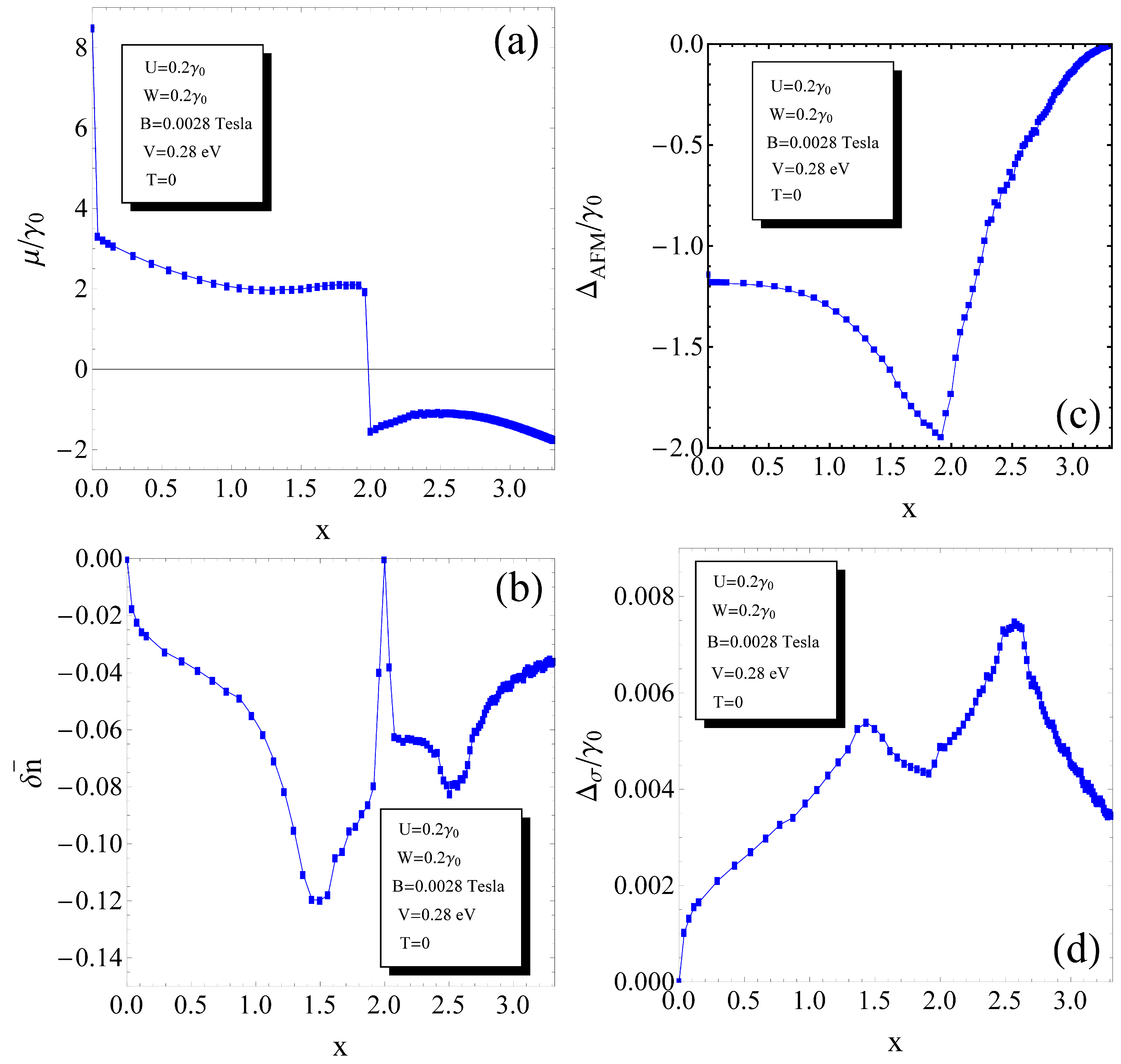
In Figure 4, we have calculated the doping dependence of the physical quantities shown in Figure 3 and Figure 4. We see in Figure 4a that there exists some critical value of doping x c = 2 at which the chemical potential has a drastic jump from positive to negative values. At the same value of doping the average charge density difference vanishes (see Figure 4b) and the system is in the charge neutrality limit: δ n ¯ = 0 . Another charge neutrality is at full filling limit x = 0 (or κ = κ min ) when the chemical potential is very high. At x = x c the antiferromagnetic order parameter Δ AFM shown in Figure 4c has a strong minimum and excitonic order parameter shown in Figure 4d also has a minimum value between two pronounced peaks at large doping x = x 1 = 1.43 and x = x 2 = 2.57 . An interesting observation from Figure 4b,d is that the maxima of the excitonic order parameter at x = x 1 and x = x 2 correspond to the larges deviations of the average charge density difference function δ n ¯ from the charge neutrality value δ n ¯ = 0 . At x = x 1 we have δ n ¯ = 0.119 and at x = x 2 we get δ n ¯ = 0.0797 . Thus, strong charge imbalance between the average electron concentrations in different layers enhances the excitonic pairing in the system. The chemical potential also experiences a minimum at x = x 1 and a maximum at x = x 2 .
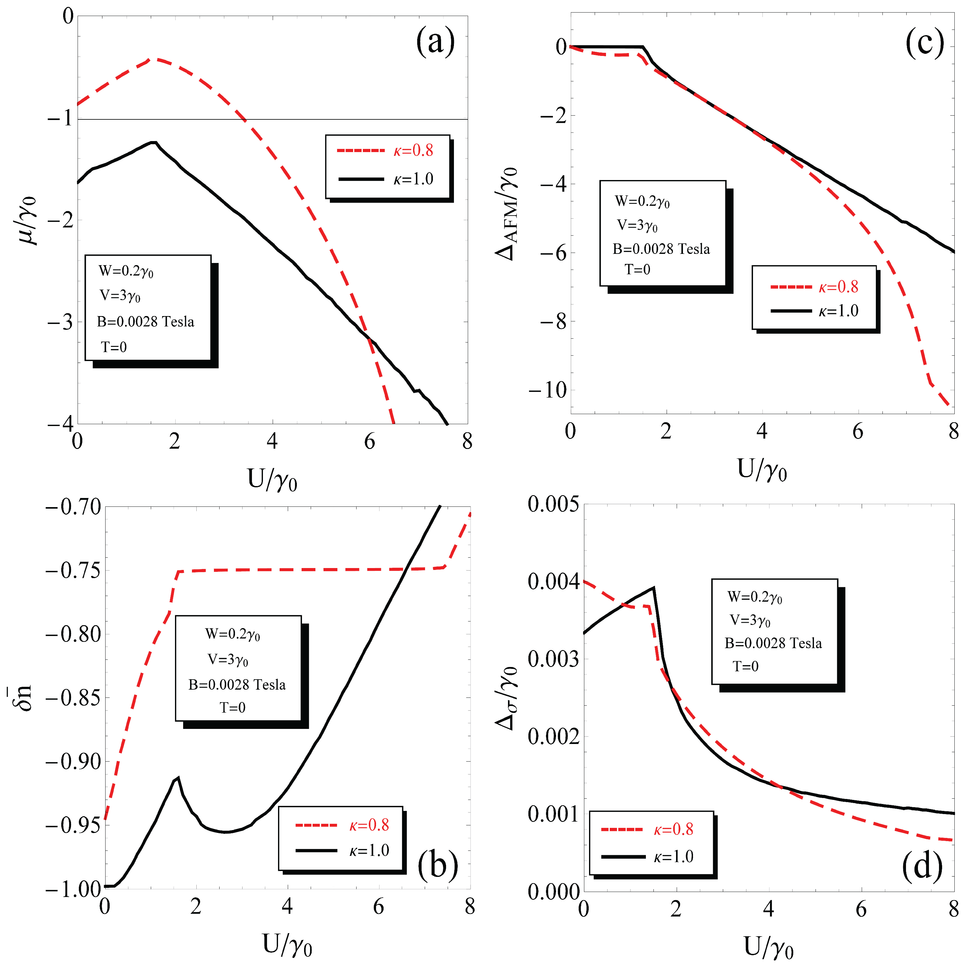
In Figure 5, we calculated the physical quantities, discussed above, as a function of the intra-layer Hubbard interaction parameter U. Two different values of the filling coefficient have been considered: κ = 0.8 (see the red dashed curve) and κ = 1 (see black solid line). We see that the behavior of the average charge density difference is completely different for these two cases. For κ = 0.8 we have δ n ¯ = c o n s t = 0.75 within a large interval of values of the Coulomb interaction parameter U 1.6 γ 0 , 7.5 γ 0 , i.e., for small doping the charge stability becomes more probable than for the large doping case (see the black curve in Figure 5b. We see in Figure 5c that strong antiferromagnetic order is enhanced for the large values of the Coulomb interaction parameter. Meanwhile, the excitonic gap parameters decrease for the large values of U (see in Figure 5d). This is due to the strong localization of the electrons and their spins at the large values of U.

4. Conclusions

In this paper, we have investigated the key physical properties of AB-stacked bilayer graphene under the combined influence of orbital effects induced by a perpendicular weak magnetic field and an electric field applied across the bilayer. The main focus has been placed on the modification of the electronic dispersion relation due to the orbital effect of the magnetic field, which is incorporated into the calculations via the Peierls phase. The coupling to the external electric field is treated through induced electric field potentials originating from the Lorentz potential in the graphene layers.
The effective electric field potentials acting on the layers are derived as functions of the externally applied voltages for different magnetic-field strengths, and good agreement with experimental results is found. Furthermore, the layer-resolved potentials are analyzed as functions of the applied magnetic field for different values of the electronic orbital quantum number arising from Landau-level quantization in reciprocal space. We find that, for large values of the Landau-level index n, the effective layer potentials exhibit a more pronounced dependence on the magnetic field.
We consider both canted staggered antiferromagnetic order and inter-layer excitonic pairing in the AB-stacked bilayer graphene system. Using numerical calculations, we evaluate the chemical potential, the average charge density imbalance between the layers, and the antiferromagnetic and excitonic order parameters as functions of the applied voltage (Figure 3), doping level (Figure 4), and local intralayer Coulomb interaction strength (Figure 5). We demonstrate that the energy scales associated with the antiferromagnetic order are several orders of magnitude larger than those associated with excitonic pairing (see Figure 3c,d, Figure 4c,d, and Figure 5c,d). The coexistence and competition between these two orders are observed across all considered parameters regimes.
For intermediate doping levels and small values of the Hubbard interaction, the antiferromagnetic order survives only in the vicinity of zero applied electric field. As either the doping level or the Hubbard interaction strength increases, an additional localized antiferromagnetic state emerges at finite applied electric fields. In this regime, the average electron density difference between the layers exhibits step-like behavior as a function of the applied electric field, accompanied by a symmetric population inversion when the applied voltage changes sign.
We identify a critical doping level at which the system reaches charge neutrality, characterized by a discontinuous jump of the chemical potential from positive to negative values (see in Figure 4a,b). Moreover, at low doping levels, the charge density imbalance displays step-like behavior as a function of the localization potential U (red curve in Figure 5b), indicating the existence of a stable charge plateau over a broad range of U. In contrast, at high doping levels, the charge imbalance varies continuously with U and does not stabilize.
The antiferromagnetic order parameter exceeds the excitonic gap by approximately three orders of magnitude and reaches large negative values in the strong-coupling limit, whereas the excitonic order parameter decreases monotonically with increasing U. This behavior reflects the localization effect induced by the Hubbard interaction (see Figure 5c,d).
Overall, the results presented in this work reveal new aspects of the interplay between orbital magnetic effects, electronic correlations, and electric-field control in AB-stacked bilayer graphene, and they may provide useful guidance for future experimental investigations of this system.

Author Contributions

Methodology, V.A. and T.K.; formal analysis, T.K.; investigation, V.A.; writing—review and editing, V.A. All authors have read and agreed to the published version of the manuscript.

Funding

This research received no external funding.

Data Availability Statement

No new data were created or analyzed in this study.

Conflicts of Interest

The authors declare no conflicts of interest.

Appendix A. The Calculation of Important Averages and Coefficients

In order to calculate the averages in Equations (15), (20), and (24), we write the partition function of the system and we introduce the source terms J σ k , ν n and J ¯ σ k , ν n as the Nambu vectors for the considered problem. Namely,
J σ k , ν n = J a σ k , ν n J b σ k , ν n J a ˜ σ k , ν n J b ˜ σ k , ν n .
Corresponding complex conjugate spinor is denoted as
J ¯ σ k , ν n = J ¯ a σ k , ν n , J ¯ b σ k , ν n , J ¯ a ˜ σ k , ν n , J ¯ b ˜ σ k , ν n .
Then, the partition function of the system is
Z = D Ψ ¯ σ D Ψ σ e S Ψ ¯ , Ψ + 1 2 k ν n , σ J ¯ σ k , ν n Ψ σ k ν n + Ψ ¯ σ k ν n J σ k , ν n = = exp 1 2 k ν n , σ J ¯ σ k ν n D ^ σ k ν n J σ k ν n ,
where, in the right-hand side we obtained an expression after matrix Hubbard–Stratonovich transformation and the matrix D ^ σ k ν n is the inverse of the matrix G = 2 β N G 1 k ν n . Then, the functional differentiation with respect to the external source fields gives the following averages
a ¯ σ k ν n a σ k ν n = 2 D 11 σ k ν n , b ¯ σ k ν n b σ k ν n = 2 D 22 σ k ν n , a ˜ ¯ σ k ν n a ˜ σ k ν n = 2 D 33 σ k ν n , b ˜ ¯ σ k ν n b ˜ σ k ν n = 2 D 44 σ k ν n , b ¯ σ k ν n a ˜ σ k ν n = 2 D 32 σ k ν n , a ˜ ¯ σ k ν n b σ k ν n = 2 D 23 σ k ν n ,
Furthermore, the system of self-consistent equations could be written as
1 β N 2 k ν n , σ D 22 σ k ν n + D 33 σ k ν n = 1 2 κ , 1 β N 2 k ν n , σ D 33 σ k ν n D 22 σ k ν n = δ n ¯ 2 , W β N 2 k ν n , σ D 23 k ν n + D 32 k ν n = Δ , W β N 2 k ν n , σ D 23 k ν n + D 32 k ν n = Δ , Δ AFM = U 4 β N 2 | k ν n , σ D 11 k ν n D 11 k ν n | + | k ν n , σ D 22 k ν n D 22 k ν n | + | k ν n , σ D 33 k ν n D 33 k ν n | + | k ν n , σ D 44 k ν n D 44 k ν n |
The components of the inverse Green’s function matrix D i j σ k ν n could be calculated directly after inverting the matrices in Equations (28) and (32). We have for the expressions under the sums, in the left hand side in Equation (A5), the following expressions
D 22 σ k ν n + D 33 σ k ν n = = β N 2 P 1 σ 3 x i = 1 4 1 x ϵ i σ k ,
where x = i ν n , and the polynomial in the nominator in the right-hand side in Equation (A6) is
P 1 σ 3 x = 2 x 3 + a 1 σ x 2 + a 2 σ k x + a 3 σ k
with the coefficients
a 1 σ = 3 μ 1 eff + μ 2 eff , a 2 σ k = 2 Δ AFM 2 + | γ k , B | 2 1 σ Δ AFM μ 1 eff μ 2 eff μ 1 eff + μ 2 eff 2 2 μ 1 eff μ 2 eff , a 3 σ k = μ 1 eff + μ 2 eff | γ k , B | 2 + Δ AFM μ 1 eff Δ AFM + μ 2 eff .
Next, we get
D 33 σ k ν n D 22 σ k ν n = = β N 2 P 2 σ 2 x i = 1 4 1 x ϵ i σ k ,
where
P 2 σ 2 x = b 1 σ x 2 + b 2 σ x + b 3 σ k ,
with the coefficients
b 1 σ = 2 1 σ Δ AFM μ 1 eff + μ 2 eff , b 2 σ = 2 1 σ Δ AFM μ 1 eff + μ 2 eff μ 1 eff 2 μ 2 eff 2 , b 3 σ k = Δ AFM + μ 1 eff Δ AFM μ 2 eff   × × 2 1 σ Δ AFM + μ 1 eff μ 2 eff + | γ k , B | 2 2 1 σ Δ AFM μ 1 eff + μ 2 eff .
The sums in the third and fourth equations in Equation (A5) are
D 23 σ k ν n + D 32 σ k ν n = = β N 2 P 3 σ 2 x i = 1 4 1 x ϵ i σ k ,
where
P 3 σ 2 x = c 1 σ x 2 + c 2 σ x + c 3 σ ,
with the coefficients
c 1 σ = 2 t + Δ σ , c 2 σ = 2 t + Δ σ μ 1 eff + μ 2 eff , c 3 σ = 2 1 σ Δ AFM μ 1 eff 1 σ Δ AFM + μ 2 eff   × × t + Δ σ .
In the last term in Equation (A5) we have for the matrix elements D 11 σ k ν n , D 22 σ k ν n , D 33 σ k ν n and D 44 σ k ν n
D 11 σ k ν n = β N 2 P 4 σ 3 x i = 1 4 1 x ϵ i σ k ,
D 22 σ k ν n = β N 2 P 5 σ 3 x i = 1 4 1 x ϵ i σ k ,
D 33 σ k ν n = β N 2 P 6 σ 3 x i = 1 4 1 x ϵ i σ k ,
D 44 σ k ν n = β N 2 P 7 σ 3 x i = 1 4 1 x ϵ i σ k ,
where the polynomials P 4 σ 3 , P 5 σ 3 , P 6 σ 3 , and P 7 σ 3 are given as
P 4 σ 3 = x 3 + d 1 σ x 2 + d 2 σ k x + d 3 σ k ,
d 1 σ = 1 σ Δ AFM μ 1 eff 2 μ 2 eff , d 2 σ k = Δ AFM 2 + t 2 + | Δ σ | 2 + | γ k , B | 2 + 2 t Δ σ , μ 2 eff 2 1 σ Δ AFM + μ 1 eff + μ 2 eff d 3 σ k = | γ k , B | 2 1 σ Δ AFM + μ 1 eff   + + 1 σ Δ AFM + μ 2 eff Δ AFM 2 + t 2 + | Δ σ | 2 + 2 t Δ σ + 1 σ Δ AFM μ 1 eff μ 2 eff μ 1 eff μ 2 eff ,
P 5 σ 3 = x 3 + e 1 σ x 2 + e 2 σ k x + e 3 σ k ,
e 1 σ = 1 σ Δ AFM μ 1 eff 2 μ 2 eff , e 2 σ k = Δ AFM 2 + | γ k , B | 2 + μ 2 eff 2 1 σ Δ AFM 2 μ 1 eff μ 2 eff , e 3 σ k = 1 σ Δ AFM μ 1 eff   × × Δ AFM 2 + | γ k , B | 2 μ 2 eff 2 ,
P 6 σ 3 = x 3 + f 1 σ x 2 + f 2 σ k x + f 3 σ k ,
f 1 σ = 1 σ Δ AFM 2 μ 1 eff μ 2 eff , f 2 σ k = Δ AFM 2 + | γ k , B | 2 μ 1 eff 2 1 σ Δ AFM + 2 μ 2 eff + μ 1 eff , f 3 σ k = 1 σ Δ AFM + μ 2 eff   × × Δ AFM 2 + | γ k , B | 2 μ 1 eff 2 ,
P 7 σ 3 = x 3 + g 1 σ x 2 + g 2 σ k x + g 3 σ k ,
g 1 σ = 1 σ Δ AFM 2 μ 1 eff μ 2 eff , g 2 σ k = Δ AFM 2 + t 2 + | Δ σ | 2 + | γ k , B | 2 + 2 t Δ σ , μ 1 eff 2 1 σ Δ AFM + μ 2 eff + μ 1 eff g 3 σ k = | γ k , B | 2 1 σ Δ AFM + μ 2 eff   + 1 σ Δ AFM μ 1 eff Δ AFM 2 + t 2 + | Δ σ | 2 + 2 t Δ σ + 1 σ Δ AFM μ 1 eff μ 2 eff μ 1 eff μ 2 eff ,
Furthermore, we perform the summations over the fermionic Matsubara frequencies ν n in Equation (A5) and we get the system of self-consistent equations in Equation (35). The α i j σ in Equation (35) are
α 1 i σ = 1 i + 1 ϵ 1 σ ( k ) ϵ 2 σ ( k ) j = 3 , 4 P 1 σ 3 ϵ i σ ( k ) ϵ i σ ( k ) ϵ j σ ( k ) , i f i = 1 , 2 . 1 i + 1 ϵ 3 σ ( k ) ϵ 4 σ ( k ) j = 1 , 2 P 1 σ 3 ϵ i σ ( k ) ϵ i σ ( k ) ϵ j σ ( k ) , i f i = 3 , 4 ,
α 2 i σ = 1 i + 1 ϵ 1 σ ( k ) ϵ 2 σ ( k ) j = 3 , 4 P 2 σ 2 ϵ i σ ( k ) ϵ i σ ( k ) ϵ j σ ( k ) , i f i = 1 , 2 . 1 i + 1 ϵ 3 σ ( k ) ϵ 4 σ ( k ) j = 1 , 2 P 2 σ 2 ϵ i σ ( k ) ϵ i σ ( k ) ϵ j σ ( k ) , i f i = 3 , 4 ,
α 3 i σ = 1 i + 1 ϵ 1 σ ( k ) ϵ 2 σ ( k ) j = 3 , 4 P 3 σ 2 ϵ i σ ( k ) ϵ i σ ( k ) ϵ j σ ( k ) , i f i = 1 , 2 . 1 i + 1 ϵ 3 σ ( k ) ϵ 4 σ ( k ) j = 1 , 2 P 3 σ 2 ϵ i σ ( k ) ϵ i σ ( k ) ϵ j σ ( k ) , i f i = 3 , 4 ,
α 4 i σ = 1 i + 1 ϵ 1 σ ( k ) ϵ 2 σ ( k ) j = 3 , 4 P 4 σ 3 ϵ i σ ( k ) ϵ i σ ( k ) ϵ j σ ( k ) , i f i = 1 , 2 . 1 i + 1 ϵ 3 σ ( k ) ϵ 4 σ ( k ) j = 1 , 2 P 4 σ 3 ϵ i σ ( k ) ϵ i σ ( k ) ϵ j σ ( k ) , i f i = 3 , 4 ,
α 5 i σ = 1 i + 1 ϵ 1 σ ( k ) ϵ 2 σ ( k ) j = 3 , 4 P 5 σ 3 k , ϵ i σ ( k ) ϵ i σ ( k ) ϵ j σ ( k ) , i f i = 1 , 2 . 1 i + 1 ϵ 3 σ ( k ) ϵ 4 σ ( k ) j = 1 , 2 P 5 σ 3 k , ϵ i σ ( k ) ϵ i σ ( k ) ϵ j σ ( k ) , i f i = 3 , 4 .
α 6 i σ = 1 i + 1 ϵ 1 σ ( k ) ϵ 2 σ ( k ) j = 3 , 4 P 6 σ 3 k , ϵ i σ ( k ) ϵ i σ ( k ) ϵ j σ ( k ) , i f i = 1 , 2 . 1 i + 1 ϵ 3 σ ( k ) ϵ 4 σ ( k ) j = 1 , 2 P 6 σ 3 k , ϵ i σ ( k ) ϵ i σ ( k ) ϵ j σ ( k ) , i f i = 3 , 4 .
α 7 i σ = 1 i + 1 ϵ 1 σ ( k ) ϵ 2 σ ( k ) j = 3 , 4 P 7 σ 3 k , ϵ i σ ( k ) ϵ i σ ( k ) ϵ j σ ( k ) , i f i = 1 , 2 . 1 i + 1 ϵ 3 σ ( k ) ϵ 4 σ ( k ) j = 1 , 2 P 7 σ 3 k , ϵ i σ ( k ) ϵ i σ ( k ) ϵ j σ ( k ) , i f i = 3 , 4 .

References

  1. Castro Neto, A.H.; Guinea, F.; Peres, N.M.R.; Novoselov, K.S.; Geim, A.K. The electronic properties of graphene. Rev. Mod. Phys. 2009, 81, 109–162. [Google Scholar] [CrossRef]
  2. Min, H.; Abergel, D.S.L.; Hwang, E.H.; Das Sarma, S. Optical and transport gaps in gated bilayer graphene. Phys. Rev. B 2009, 2011, 041406. [Google Scholar] [CrossRef]
  3. Ashok, K.S.; Isaac, L.; Yash, R.P.; Harry, E.; Pradeep, H.; Nibir, K.D.; Jay, L.; Madan, D.; Eugene, Z.; Priyalal, W.; et al. Review of Graphene Technology and Its Applications for Electronic Devices. In Graphene; Ebrahimi, F., Ed.; IntechOpen: Rijeka, Croatia, 2015; Chapter 3. [Google Scholar]
  4. Sun, Y.; Sun, M.; Xie, D. 5-Graphene Electronic Devices. In Graphene; Zhu, H., Xu, Z., Xie, D., Fang, Y., Eds.; Academic Press: Cambridge, MA, USA, 2018. [Google Scholar]
  5. Edward, M. Asymmetry gap in the electronic band structure of bilayer graphene. Phys. Rev. B 2006, 74, 161403. [Google Scholar] [CrossRef]
  6. Youngjoon, C.; Jeannette, K.; Yang, P.; Thomson, A.; Arora, H.; Polski, R.; Zhang, Y.; Ren, H.; Alicea, J.; Refael, G.; et al. Electronic correlations in twisted bilayer graphene near the magic angle. Nat. Phys. 2019, 15, 1174–1180. [Google Scholar]
  7. Hadipour, H.; Jafari, S.A. The importance of electron correlation in graphene and hydrogenated graphene. Eur. Phys. J. B 2015, 88, 270. [Google Scholar] [CrossRef]
  8. Sengupta, J.; Hussain, C.M. Graphene-Induced Performance Enhancement of Batteries, Touch Screens, Transparent Memory, and Integrated Circuits: A Critical Review on a Decade of Developments. Nanomaterials 2022, 12, 3146. [Google Scholar] [CrossRef]
  9. Mak, K.F.; Lui, C.H.; Shan, J.; Heinz, T.F. Observation of an Electric-Field-Induced Band Gap in Bilayer Graphene by Infrared Spectroscopy. Phys. Rev. Lett. 2009, 102, 256405. [Google Scholar] [CrossRef]
  10. Abdullah, H.M.; El Mouhafid, A.; Shukla, G.; Schwingenschlögl, U. Dual-gated bilayer graphene with layer mismatch. Phys. Rev. B 2023, 108, 155434. [Google Scholar] [CrossRef]
  11. Saleem, Y.; Sadecka, K.; Korkusinski, M.; Miravet, D.; Dusko, A.; Hawrylak, P. Theory of Excitons in Gated Bilayer Graphene Quantum Dots. Nano Lett. 2023, 23, 2998–3004. [Google Scholar] [CrossRef]
  12. Du, M.; Du, L.; Wei, N.; Liu, W.; Bai, X.; Sun, Z. Dual-gated mono–bilayer graphene junctions. Nanoscale Adv. 2021, 3, 399–406. [Google Scholar] [CrossRef]
  13. Goerbig, M.O. Electronic properties of graphene in a strong magnetic field. Rev. Mod. Phys. 2011, 83, 1193–1243. [Google Scholar] [CrossRef]
  14. Peierls, R. Zur Theorie des Diamagnetismus von Leitungselektronen. Z. Phys. 1933, 80, 763–791. [Google Scholar] [CrossRef]
  15. Cresti, A. Convenient Peierls phase choice for periodic atomistic systems under magnetic field. Phys. Rev. B 2021, 103, 045402. [Google Scholar] [CrossRef]
  16. Ou, Y.C.; Chiu, Y.H.; Lin, M.F. Electronic properties of monolayer graphene in the presence of the uniform magnetic and modulated electric fields. Diam. Relat. Mater. 2010, 19, 604–607. [Google Scholar] [CrossRef]
  17. Marconcini, P.; Macucci, M. Effects of A Magnetic Field on the Transport and Noise Properties of a Graphene Ribbon with Antidots. Nanomaterials 2020, 10, 2098. [Google Scholar] [CrossRef]
  18. Martínez-Moreno, D.I.; Negro, J.; Nieto, L.M. Polar coherent states in bilayer graphene under a constant uniform magnetic field. Phys. Lett. A 2024, 494, 129301. [Google Scholar] [CrossRef]
  19. Apinyan, V.; Kopeć, T. Magnetic Field-Controlled Electrical Conductivity in AA Bilayer Graphene. C 2023, 9, 42. [Google Scholar] [CrossRef]
  20. Nicol, E.J.; Carbotte, J.P. Optical conductivity of bilayer graphene with and without an asymmetry gap. Phys. Rev. B 2008, 77, 155409. [Google Scholar] [CrossRef]
  21. Wang, Y.; Wang, H.; Gao, J.-H.; Zhang, F.-C. Layer antiferromagnetic state in bilayer graphene: A first-principles investigation. Phys. Rev. B 2013, 87, 195413. [Google Scholar] [CrossRef]
  22. Kharitonov, M. Antiferromagnetic state in bilayer graphene. Phys. Rev. B 2012, 86, 195435. [Google Scholar] [CrossRef]
  23. Sboychakov, A.O.; Rozhkov, A.V.; Rakhmanov, A.L. Triplet superconductivity and spin density wave in biased AB bilayer graphene. Phys. Rev. B 2023, 108, 184503. [Google Scholar] [CrossRef]
  24. Rakhmanov, A.L.; Rozhkov, A.V.; Sboychakov, A.O.; Nori, F. Half-metal and other fractional metal phases in doped AB bilayer graphene. Phys. Rev. B 2023, 107, 155112. [Google Scholar] [CrossRef]
  25. Mohammadzadeh, L.; Shojaei, S.; Ahmadi, E.; Asgari, A. Excitonic effects of bilayer graphene: A simple approach. Optik 2013, 124, 6126–6131. [Google Scholar] [CrossRef]
  26. Apinyan, V.; Kopeć, T.K. Excitonic gap formation and condensation in the bilayer graphene structure. Phys. Scr. 2016, 91, 095801. [Google Scholar] [CrossRef][Green Version]
  27. Owerre, S.A. Magnon Hall effect in AB-stacked bilayer honeycomb quantum magnets. Phys. Rev. B 2016, 94, 094405. [Google Scholar] [CrossRef]
  28. Prayitno, T.B. Magnon energies and thermoelectric properties of AB-stacked bilayer zigzag graphene nanoribbons. Phys. Scr. 2025, 100, 075930. [Google Scholar] [CrossRef]
  29. Yin, L.-J.; Bai, K.-K.; Wang, W.-X.; Li, S.-Y.; Zhang, Y.; He, L. Landau quantization of Dirac fermions in graphene and its multilayers. Front. Phys. 2017, 12, 127208. [Google Scholar] [CrossRef]
  30. Plochocka, P.; Faugeras, C.; Orlita, M.; Sadowski, M.L.; Martinez, G.; Potemski, M.; Goerbig, M.O.; Fuchs, J.-N.; Berger, C.; de Heer, W.A. High-Energy Limit of Massless Dirac Fermions in Multilayer Graphene using Magneto-Optical Transmission Spectroscopy. Phys. Rev. Lett. 2008, 100, 087401. [Google Scholar] [CrossRef]
  31. Bessler, R.; Duerig, U.; Koren, E. The dielectric constant of a bilayer graphene interface. Nanoscale Adv. 2019, 1, 1702–1706. [Google Scholar] [CrossRef]
  32. Apinyan, V.; Kopeć, T.K. Canted antiferromagnetism and excitonic order in gated double-layer graphene. Phys. Rev. B 2023, 108, 075147. [Google Scholar] [CrossRef]
  33. Pereira, V.M.; Hardt, L.G.; Fantineli, D.G.; Heckler, M.V.T.; Armas, L.E.G. Characterization of Dielectric Properties of Graphene and Graphite Using the Resonant Cavity in 5G Test Band. J. Microw. Optoelectron. Electromagn. Appl. 2023, 22, 1. [Google Scholar] [CrossRef]
  34. Negele, J.W.; Orland, H. Quantum Many-Particle Systems; Westview Press: Boulder, CO, USA, 1998. [Google Scholar]
  35. Powell, M.J.D. A hybrid method for nonlinear equations. In Numerical Methods for Nonlinear Algebraic Equations; Gordon and Breach: London, UK, 1970; pp. 87–161. [Google Scholar]
Figure 1. Staggering canted antiferromagnetic order in the AB bilayer graphene system. The antiferromagnetic order parameter is shown at each sublattice atomic site positions A, B (in the bottom layer = 1 ), A ˜ and B ˜ (in the top layer = 2 ) in the AB bilayer. The order parameter Δ AFM is defined in Equation (20).
Crystals 16 00095 g001
Figure 2. Panel (a): Dependence of the acting electric field potential in the layers V act ( = 1 , 2 ) on the applied electric field potential V. Different values of the magnetic field have been considered. Panel (b): Dependence of the acting electric field potential in the layers on the external magnetic field, for different values of the quantum number n and for the fixed value of the applied electric field potential V = 0.28 eV.
Crystals 16 00095 g002
Figure 3. External field dependence of the calculated physical quantities. The calculations have been done for W = 0.2 γ 0 , B = 0.0028 T, n = 2 and T = 0 . In panels (ad), we plotted the chemical potential μ , charge density difference δ n ¯ , antiferromagnetic order parameter Δ AFM and excitonic order parameters Δ σ . Different values of the Hubbard-U interaction and filling coefficient κ have been employed.
Crystals 16 00095 g003
Figure 4. Doping dependence of the calculated physical quantities. The calculations have been done for U = 0.2 γ 0 = 0.56 eV, W = 0.2 γ 0 = 0.56 eV, B = 0.0028 T, V = 0.28 eV and T = 0 . In panels (ad), we plotted the chemical potential μ , charge density difference δ n ¯ , antiferromagnetic order parameter Δ AFM and excitonic order parameters Δ σ .
Crystals 16 00095 g004
Figure 5. In panels (ad), we plotted the chemical potential μ , charge density difference δ n ¯ , antiferromagnetic order parameter Δ AFM and excitonic order parameters Δ σ as a function of the intra-layer Hubbard-U interaction. Two different values of the filling factor have been considered: κ = 0.8 (see the red dashed curve) and κ = 1 (see solid black line). The calculations have been done for W = 0.2 γ 0 = 0.56 eV, B = 0.0028 T, V = 3 γ 0 eV and T = 0 .
Crystals 16 00095 g005
Disclaimer/Publisher’s Note: The statements, opinions and data contained in all publications are solely those of the individual author(s) and contributor(s) and not of MDPI and/or the editor(s). MDPI and/or the editor(s) disclaim responsibility for any injury to people or property resulting from any ideas, methods, instructions or products referred to in the content.