1. Introduction
Zinc oxide (ZnO), a representative third-generation wide-bandgap semiconductor, exhibits promising applications in optoelectronics due to its excellent physical and chemical properties [
1,
2]. As a direct bandgap (3.37 eV) II-VI semiconductor, its high exciton binding energy (60 meV) enables efficient room-temperature ultraviolet stimulated emission [
3,
4,
5]. Doping with elements such as Al or In yields n-type transparent conductive films with over 90% visible-light transmittance [
6,
7,
8,
9,
10]. These characteristics make ZnO an ideal material for ultraviolet detectors, LEDs, and lasers [
11,
12,
13,
14].
ZnO possesses one of the richest families of nanostructures, including nanowires [
15,
16], nanobelts [
17], nanorings [
18], and more. Different applications require specific morphologies, making controlled synthesis paramount [
19,
20,
21]. Current synthesis methods primarily include liquid-phase and vapor-phase techniques. While liquid-phase methods offer advantages like low cost and mild reaction conditions, they often suffer from limited product purity. In contrast, vapor transport methods (e.g., PLD [
22], MBE [
23], MOCVD [
24]) provide higher efficiency and yield, representing a viable route for industrial production.
Among vapor-phase techniques, the vapor–liquid–solid (VLS) mechanism is crucial for growing ZnO nanowires, where catalyst properties (e.g., size, distribution) critically influence the final morphology and dimensions [
25]. However, the VLS mechanism is highly sensitive to experimental parameters, and fundamental aspects such as the annealing process of catalysts (e.g., Au films) remain insufficiently explored, hindering the controlled preparation of ZnO nanostructures. Therefore, this study aims to investigate the synthesis of ZnO nanostructures via the VLS mechanism using a custom-built vapor transport system. We focus on elucidating the effects of various experimental parameters on product morphology to deepen the understanding of the growth mechanism and provide experimental and theoretical foundations for the controlled preparation and application of ZnO nanostructures.
2. Experimental Details
Silicon substrates were sequentially ultrasonically cleaned in acetone and ethanol for 20 min each, rinsed with deionized water, and dried with nitrogen. A thin gold (Au) film was deposited onto the pre-treated Si substrates using a dual-tilt electron beam evaporation system (JEB-2). The deposition was carried out under a base pressure of 10−4 Pa to minimize contamination, with a constant deposition rate of 3 Å/s maintained to ensure uniform film formation. This Au layer served as the catalyst for the subsequent growth of ZnO nanostructures.
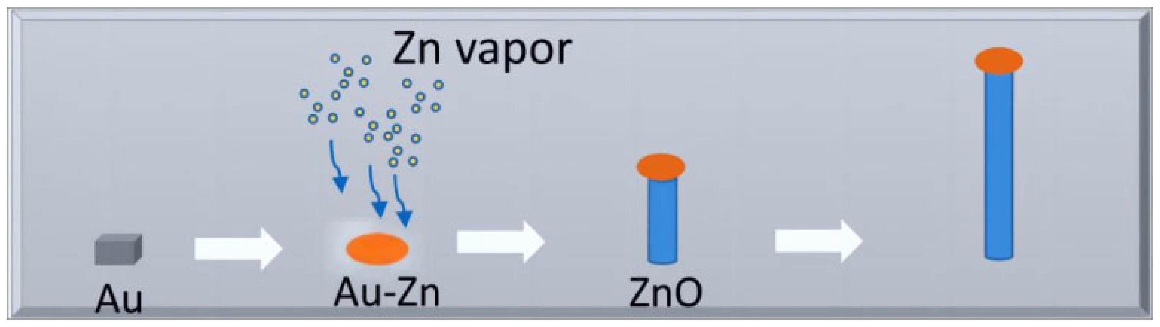
The experimental setup utilizes a custom high-temperature tube furnace (OTF-1200X-III, Hefei Kejing Material Technology Co., Ltd., Hefei, China) with a three-zone independent heating system, where the temperature profile along the quartz tube is precisely controlled to create a stable gradient. As illustrated in
Figure 1, high-purity zinc oxide (ZnO) powder and carbon black were mixed in a 1:1 mass ratio (0.6 g ZnO and 0.6 g carbon black), thoroughly ground, and placed in a quartz boat positioned at the center of the heating zone in a high-temperature tube furnace. The Au/Si substrate was placed approximately 10 cm downstream. The system pressure was first evacuated below 0.1 Pa using a mechanical pump. A mixed carrier gas (Ar/O
2) with a total flow rate of 50 sccm was then introduced, maintaining the system pressure between 150 Pa and 5000 Pa. This was achieved by dynamically balancing the gas inlet flow via mass flow controllers with an exhaust throttle valve at the downstream, ensuring stable vapor-phase transport conditions essential for reproducible VLS growth. The furnace was heated to the set temperature at a rate of 50 °C/min and maintained for 30 min. After growth, the carrier gas flow was stopped, and the sample was allowed to cool naturally to room temperature before removal. Key parameters (Au catalyst, growth temperature, system pressure, and oxygen ratio) were systematically varied to study their interactions, quantify their impact on ZnO nanostructure growth, and reveal underlying relationships to optimize synthesis conditions.
The synthesized ZnO nanostructures were characterized using scanning electron microscopy (SEM, GeminiSEM 300, Zeiss, Jena, Germany), transmission electron microscopy (TEM, Titan Themis G2, Thermo Fisher Scientific, Hillsboro, OR, USA), X-ray diffraction (XRD, Rigaku, Tokyo, Japan), and photoluminescence (PL, Horiba iHR 320 PL, Horiba Scientific, Kyoto, Japan) spectroscopy to analyze their morphology, crystal structure, and optical properties.
3. Results and Discussion
3.1. Influence of Gold Catalyst on ZnO Nanostructures
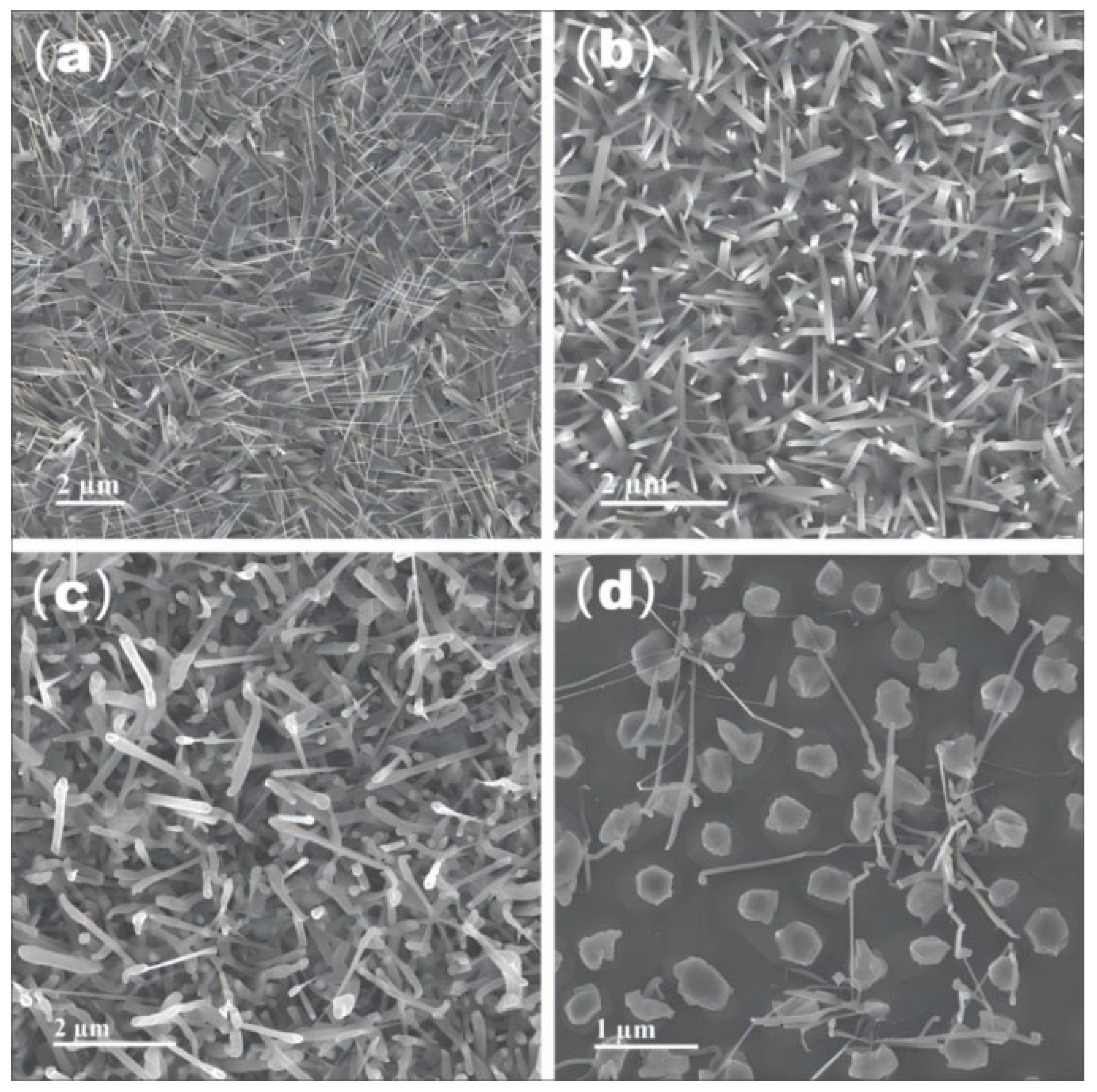
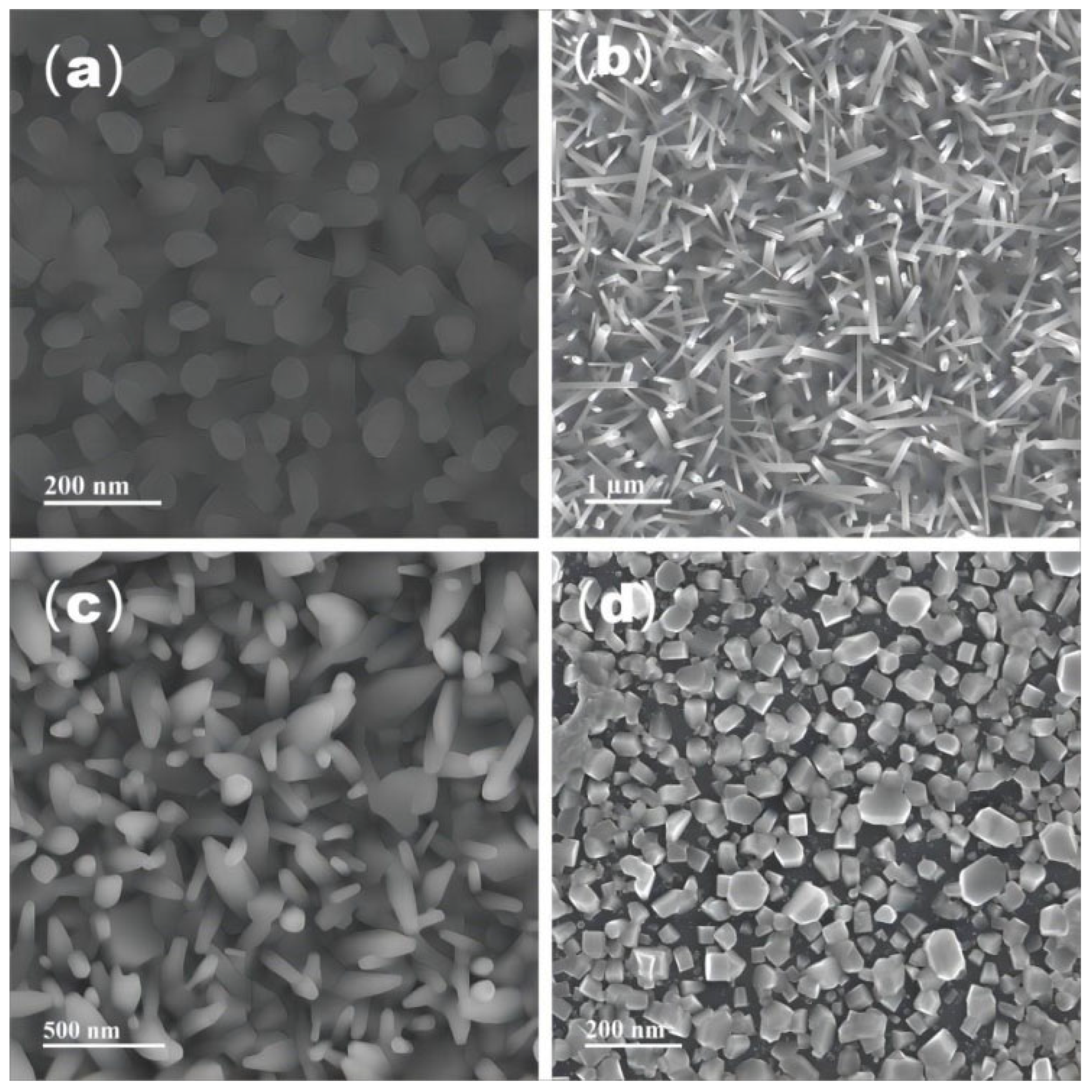
Au/Si substrates underwent either high-temperature rapid annealing or low-temperature slow annealing to form Au nanoparticles of varying sizes and densities. ZnO nanostructures were synthesized under identical conditions except for the Au film thickness (3 nm, 5 nm, 15 nm) and annealing treatment. The resulting morphologies are shown in
Figure 2.
Figure 2a,b correspond to samples with a 3 nm Au film. High-density, high-yield nanowires were observed. For high-temperature rapid annealing (900 °C, 15 s, Au nanoparticle average diameter = 52 ± 3 nm), the average nanowire diameter was approximately 60 nm (
Figure 2a). Low-temperature slow annealing (400 °C, 30 min, Au nanoparticle average diameter = 70 ± 4 nm) resulted in larger average diameters of about 84 nm (
Figure 2b). With a 5 nm Au film under high-temperature rapid annealing (900 °C, 15 s, Au nanoparticle average diameter = 102 ± 6 nm), the nanowires were sparsely distributed with medium yield and an average diameter of ~130 nm (
Figure 2c). For the 15 nm Au film subjected to high-temperature rapid annealing (900 °C, 30 s, Au nanoparticle average diameter = 430 ± 25 nm), almost no nanowires formed. Instead, granular structures consisting of ZnO crystallites and Au particles were observed, with average sizes around 460 nm (
Figure 2d).
These results demonstrate the significant influence of Au catalyst properties on VLS-grown ZnO nanostructures. Quantitative analysis revealed a strong positive correlation between nanowire diameter and Au nanoparticle size (R
2 = 0.98), indicating that Au particle size directly modulates nanowire thickness. Furthermore, thicker Au films resulted in reduced nanowire yield and density, particularly evident for the 15 nm film. This can be attributed to two factors: first, thicker films yield larger, less dense Au particles after annealing; second, larger particles require a greater supply of Zn and O atoms to achieve supersaturation and nucleation, and increased diffusion distances significantly reduce growth rates, hindering the formation of complete 1D nanostructures within the 30 min growth period [
26,
27,
28]. The large ZnO grains in
Figure 2d support this inference. Notably, the average diameters of the synthesized nanowires exceeded those of the initial Au nanoparticles. This discrepancy may arise from: (i) further coarsening of Au particles at high temperatures, especially in thin films (e.g., 3 nm, 5 nm) where high initial density facilitates particle coalescence, leading to thicker nanowires; and (ii) potential radial growth of ZnO nanowires, where Au migration to the sidewalls catalyzes lateral deposition, increasing diameter.
3.2. Effect of Temperature on ZnO Nanostructures
In VLS growth, the source temperature and substrate temperature are critical parameters governing reaction kinetics and deposition, respectively [
29]. To systematically study the temperature effect, experiments were conducted by varying the source temperature while keeping other parameters constant. Based on the carbothermal reduction reaction, the theoretical reaction temperature exceeds 950 °C. The source temperature varied from 850 °C to 1100 °C, while the substrate temperature was maintained at 880 °C.
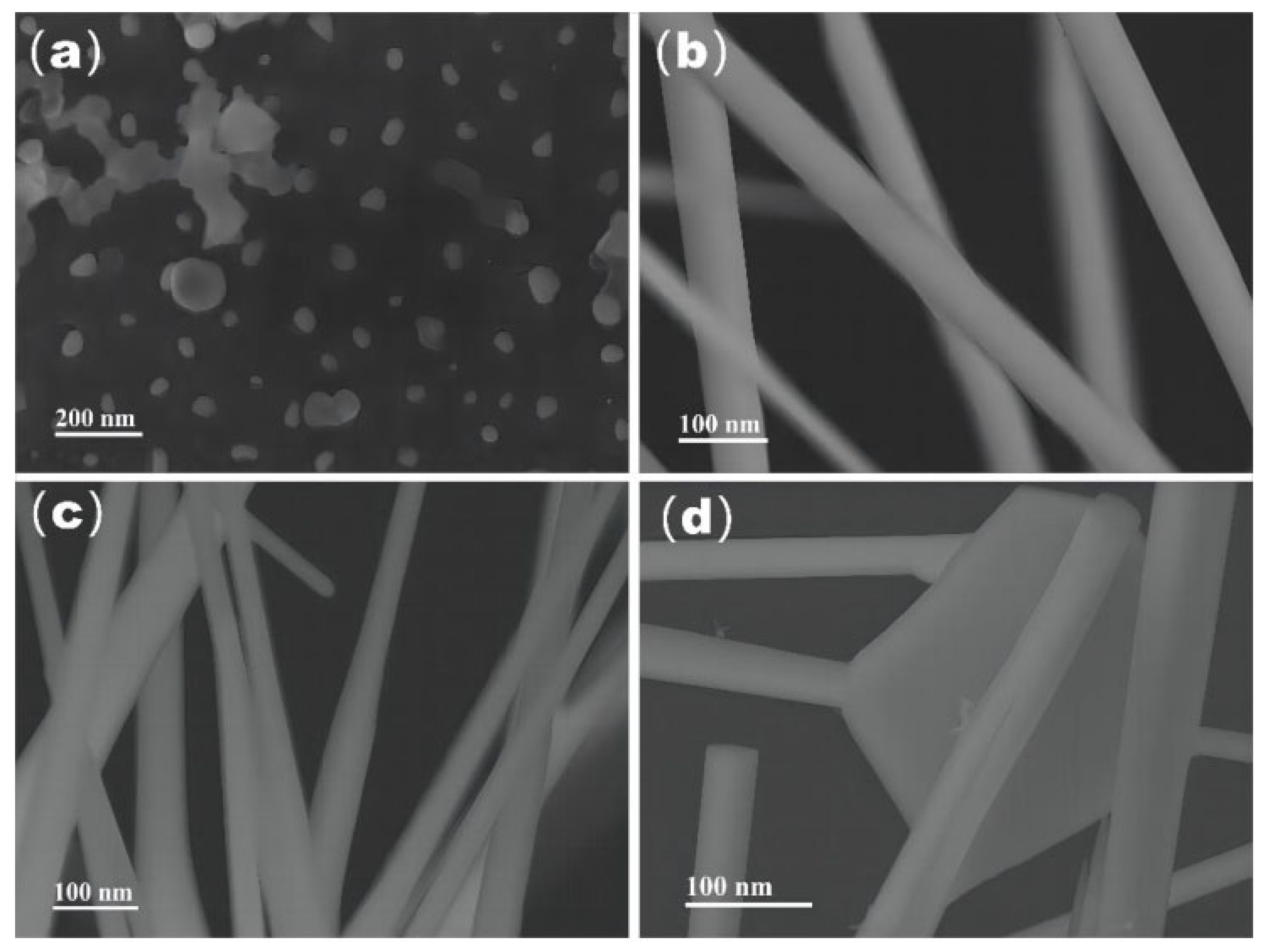
At a source temperature of 850 °C (
Figure 3a), only Au particles and sporadic ZnO grains were observed, with no well-defined nanowires, indicating insufficient Zn vapor generation for sustained VLS growth. When the source temperature reached 950 °C (
Figure 3b), significant reaction occurred, producing adequate Zn vapor for stable nanowire growth catalyzed by Au droplets. Further increasing the temperature to 1000 °C (
Figure 3c) also yielded nanowires, with slightly thinner diameters (average diameter: 55–65 nm) compared to those grown at 950 °C, suggesting that higher Zn vapor pressure enhances atomic diffusion within the droplet, favoring axial growth and yielding slenderer nanostructures. However, at an excessively high temperature of 1100 °C (
Figure 3d), the morphology transitioned to sheet-like ZnO structures, attributed to excessive Zn vapor supersaturation inducing two-dimensional nucleation and growth [
30,
31].
Thus, source temperature critically controls ZnO nanostructure morphology. Temperatures that are too low prevent nanowire growth due to insufficient reaction, while excessively high temperatures promote 2D growth, hindering the formation of uniform 1D nanostructures. Precise temperature control is therefore essential for the controlled preparation of high-quality ZnO nanowires.
3.3. Influence of System Pressure on ZnO Nanostructures
The growth of ZnO nanostructures under vapor transport conditions is governed not only by the vapor generation rate but also critically by the transport dynamics and residence time of reactant species within the system. While the Zn vapor generation rate remains relatively constant at a fixed source temperature, the system pressure, coupled with the controlled carrier gas flow, primarily influences the molecular mean free path and the residence time of Zn species in the high-temperature zone and their diffusion towards the substrate [
32]. A series of syntheses were performed under a constant total carrier gas flow rate while varying the system pressure between 150 Pa and 5000 Pa. These conditions directly modulate the reactant transport efficiency and the time available for supersaturation buildup at the growth front.
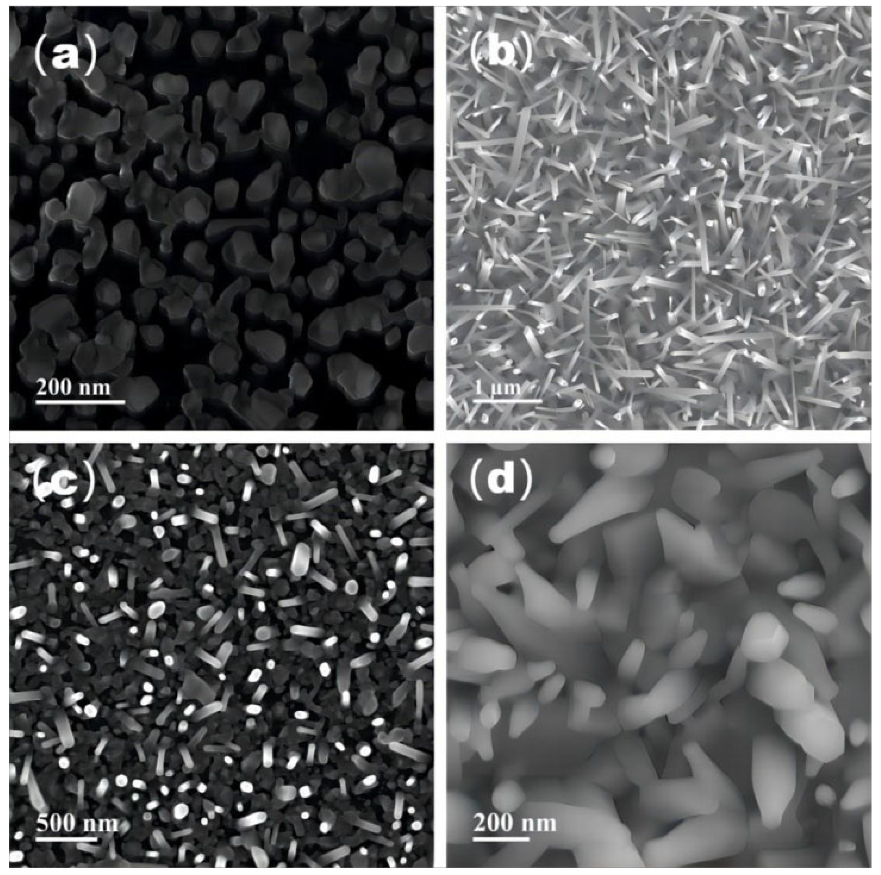
As shown in
Figure 4, at a high pressure of 5000 Pa, the product consisted mainly of Au particles and few ZnO grains, with no nanowire formation. The short residence time and reduced mean free path at this pressure likely hinder the effective transport and surface diffusion of adatoms, preventing the sustained supersaturation required for 1D nanowire growth. Reducing the pressure to 3000 Pa enhanced the vapor transport efficiency, providing conditions conducive to uniform nanowire growth via the VLS mechanism, as evidenced by the numerous nanowires with diameters of approximately 50–65 nm. At a lower pressure of 600 Pa, the increased mean free path and longer residence time promote higher adatom mobility and local supersaturation, leading to the formation of short nanorods with two-dimensional ZnO layers at their bases. When the pressure was further reduced to 150 Pa, the excessively long residence time and high adatom mobility resulted in a continuous ZnO film with attached nanorods, demonstrating a transition to predominant two-dimensional growth due to extensive surface diffusion and nucleation. These results confirm that system pressure, by governing the reactant transport dynamics and residence time rather than directly modulating a quantified partial pressure, is a key parameter determining the growth mode and final morphology of ZnO nanostructures.
3.4. Effect of Oxygen Concentration on ZnO Nanostructure
Oxygen content is a critical factor influencing the vapor transport synthesis of ZnO, as it participates in the carbothermal reduction and oxidation pathways, regulating the dynamic balance between Zn vapor generation and consumption [
33,
34]. To investigate this effect, synthesis experiments were conducted at a system pressure of 3000 Pa by varying the oxygen volume ratio (1–4%) while maintaining a total carrier gas flow of 50 sccm.
At 1% O
2 (
Figure 5a), only nucleated ZnO grains were observed, with no nanowire formation. Increasing the oxygen ratio to 2% (
Figure 5b) resulted in the abundant growth of uniform nanowires (average diameter ~ 60 nm). At 2.5% O
2 (
Figure 5c), the nanostructures transformed into short rods with significantly reduced density. Further increasing the oxygen ratio to 4% (
Figure 5d) yielded almost no nanowires, primarily producing ZnO grains and bulk aggregates. These phenomena are closely related to the competition among multiple reactions in the system, including:
Under low oxygen conditions (e.g., 1%), CO generated from reaction (2) accumulates, inhibiting the forward progress of the carbothermal reduction reaction (1), leading to insufficient Zn vapor concentration for nanowire growth. Moderately increasing the oxygen ratio (e.g., 2%) promotes reaction (3), consuming CO and driving reaction (1) forward, thereby generating sufficient Zn vapor for high-quality nanowire growth. However, excessively high oxygen concentrations (≥2.5%, 2.5% O
2 with O
2 flow rate of 1.25 sccm and Ar flow rate of 48.75 sccm) intensify reaction (4), leading to premature oxidation of Zn vapor in the source zone. Based on the vapor trapping mechanism described in prior studies, this condition may promote the formation of a ZnO shell on the source material, analogous to the ZnO structures observed under Zn-rich environments, which would hinder vapor release and reduce Zn transport to the substrate, thereby inhibiting nanowire growth [
35]. This interpretation is consistent with the observed suppression of nanowire formation at high O
2 concentrations.
In summary, moderate oxygen concentration (approximately 2%) is optimal for efficient ZnO nanowire growth. Both excessively high and low oxygen levels disrupt the reaction equilibrium, adversely affecting morphology and yield.
4. Morphology, Structure, and Optical Properties of ZnO Nanowires Under Optimized Conditions
This study demonstrates that synergistic optimization of key parameters, such as Au catalyst thickness, source temperature, system pressure, and oxygen content, enables controlled growth of ZnO nanowires via the VLS method. As shown in
Table 1, unlike previous VLS/CVT studies that often focus on isolated factors, our work provides a comprehensive parameter mapping with mechanistic insights, particularly highlighting how pressure modulates Zn vapor supersaturation and oxygen balance’s reaction kinetics. Under optimized conditions (3 nm Au film, source temperature 950 °C, O
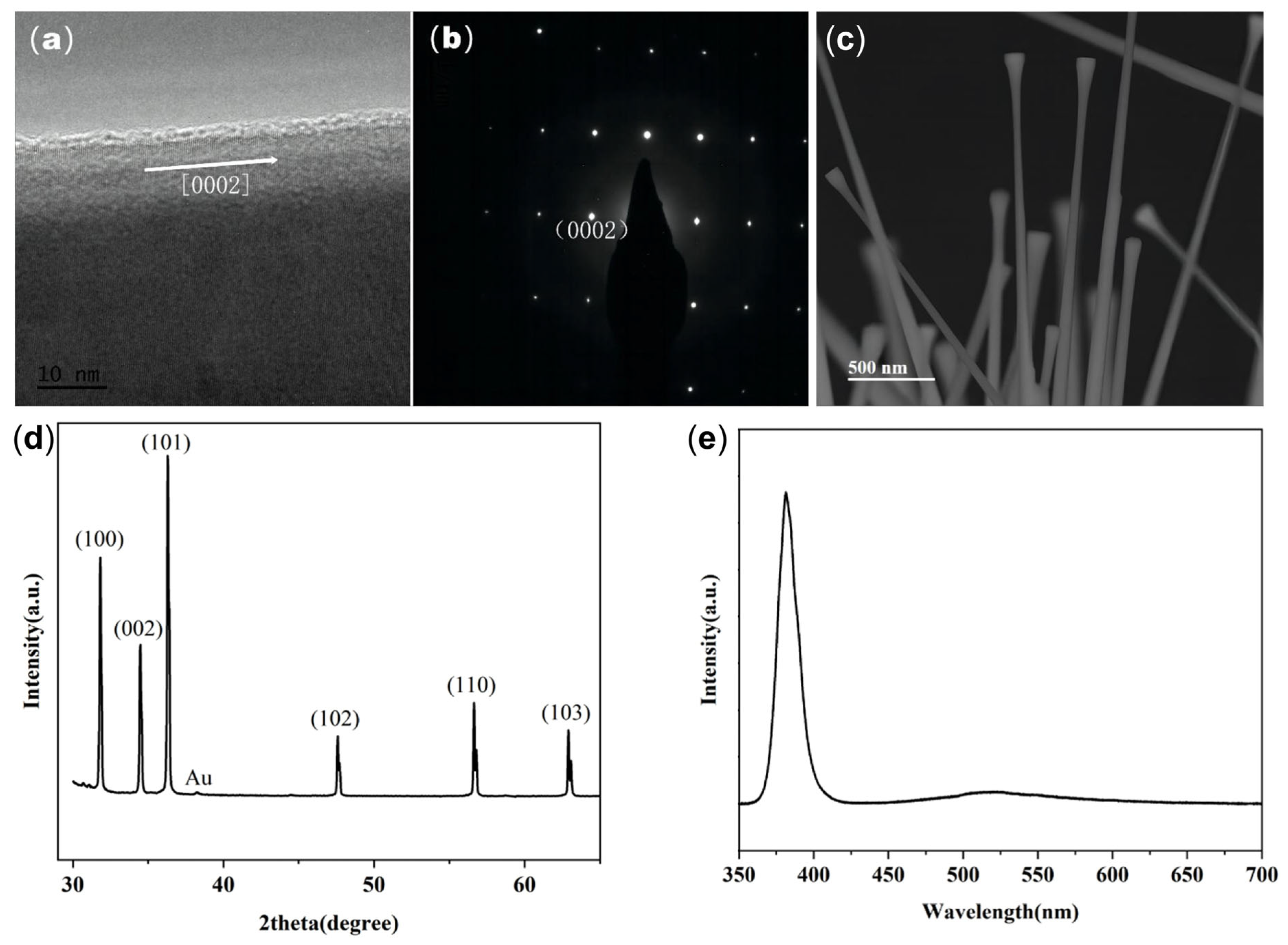
2 2 vol%, system pressure 3000 Pa), ZnO nanowires with excellent morphological and structural properties were achieved. These outcomes are validated by the characterization results shown in
Figure 6.
High-resolution TEM images (
Figure 6a,b) and corresponding selected-area electron diffraction (SAED) patterns clearly revealed the crystalline structure. Continuous lattice fringes and sharp diffraction spots confirmed the single-crystalline nature of the nanowires, growing along the [0001] direction. SEM images (
Figure 6c) showed uniform nanowire morphology with an average diameter of approximately 60 nm and a length of approximately 2 μm. The XRD pattern (
Figure 6d) was acquired using a Cu Kα radiation source (λ = 1.5406 Å) with a scan range from 30° to 70° (2θ). Rietveld refinement of the pattern confirmed the hexagonal wurtzite structure of ZnO (JCPDS No. 36-1451), with the three dominant diffraction peaks precisely located at 31.77°, 34.42°, and 36.25°, corresponding to the (100), (002), and (101) crystal planes, respectively. An additional peak was observed at 38.18°, which is indexed to the (111) plane of metallic Au (JCPDS No. 04-0784), further corroborating the VLS growth mode. The PL spectrum (
Figure 6e) showed two emission peaks: a strong near-band-edge (NBE) emission peak centered at 380.5 nm (3.26 eV) with a full width at half maximum (FWHM) of 15 nm, and a weak, broad defect-related green emission band centered at 525 nm, originating from internal defects in ZnO. (2.36 eV) [
12,
36]. The PL measurement was performed at room temperature using a 325 nm He-Cd laser as the excitation source. The laser beam was focused on a spot size of about 100 μm in diameter, sampling an ensemble of several thousand nanowires simultaneously. The excitation was unpolarized, and the collected emission signal thus represents the average optical properties of the nanowire ensemble within the probed region, confirming the uniformity and homogeneity of the synthesized product. These results confirm the successful synthesis of high-quality, single-crystal ZnO nanowires with excellent optical properties under the optimized conditions.
5. Conclusions
This study demonstrates that thinner Au films (3–5 nm), an optimal source temperature window (950–1000 °C), controlled system pressure (~3000 Pa), and precise oxygen content (2%) synergistically influence the growth of ZnO nanowires, with the vapor–liquid–solid (VLS) mechanism playing a primary role under these optimized conditions by regulating Zn vapor supersaturation and reaction pathways. The VLS process is supported by evidence from the optimized sample: TEM images show characteristic Zn–Au alloy droplets at nanowire tips, XRD patterns reveal Au-related peaks, and EDX analysis confirms Au presence at tips. Under these parameters, well-aligned single-crystalline ZnO nanowires with high structural quality and strong near-band-edge emission were achieved. These findings establish a reproducible and controllable synthesis pathway for high-quality ZnO nanowires, paving the way for their future exploration in optoelectronic devices.
Author Contributions
Methodology, Z.-Y.L.; Resources, H.-X.L.; Writing—original draft, Z.-Y.L.; Writing—review & editing, T.-Y.C.; Supervision, T.-Y.C. All authors have read and agreed to the published version of the manuscript.
Funding
This research was funded by the Key-Area Research and Development Program of Guangdong Province (Grants Nos. 2020B0303050001, 2021B0101300001) and the National Natural Science Foundation of China (Grant No. 11974158).
Data Availability Statement
Dataset available on request from the authors.
Conflicts of Interest
The authors declare no conflicts of interest.
References
- Hu, Y.; Zhou, J.; Yeh, P.H.; Li, Z.; Wei, T.Y.; Wang, Z.L. Supersensitive, fast-response nanowire sensors by using Schottky contacts. Adv. Mater. 2010, 22, 3327–3332. [Google Scholar] [CrossRef] [Scilit]
- Li, Z.Y.; Yang, H.Z.; Chen, S.C.; Lu, Y.B.; Xin, Y.Q.; Yang, T.L.; Sun, H. Impact of active layer thickness of nitrogen-doped In–Sn–Zn–O films on materials and thin film transistor performances. J. Phys. D Appl. Phys. 2018, 51, 175101. [Google Scholar] [CrossRef] [Scilit]
- Look, D.C.; Reynolds, D.C.; Sizelove, J.; Jones, R.; Litton, C.W.; Cantwell, G.; Harsch, W. Electrical properties of bulk ZnO. Solid State Commun. 1998, 105, 399–401. [Google Scholar] [CrossRef] [Scilit]
- Yu, P.; Tang, Z.; Wong, G.K.; Kawasaki, M.; Ohtomo, A.; Koinuma, H.; Segawa, Y. Room-temperature gain spectra and lasing in microcrystalline ZnO thin films. J. Cryst. Growth 1998, 184, 601–604. [Google Scholar] [CrossRef] [Scilit]
- Alharshan, G.A.; Aboraia, A.M.; Uosif, M.A.; Sharaf, I.M.; Shaaban, E.R.; Saad, M.; ALMohiy, H.; Elsenety, M.M. Optical band gap tuning, DFT understandings, and photocatalysis performance of ZnO nanoparticle-doped Fe compounds. Materials 2023, 16, 2676. [Google Scholar] [CrossRef] [Scilit] [PubMed]
- Hu, J.; Gordon, R.G. Atmospheric pressure chemical vapor deposition of gallium doped zinc oxide thin films from diethyl zinc, water, and triethyl gallium. J. Appl. Phys. 1992, 72, 5381–5392. [Google Scholar] [CrossRef] [Scilit]
- Kim, H.; Gilmore, C.; Horwitz, J.; Pique, A.; Murata, H.; Kushto, G.; Schlaf, R.; Kafafi, Z.; Chrisey, D. Transparent conducting aluminum-doped zinc oxide thin films for organic light-emitting devices. Appl. Phys. Lett. 2000, 76, 259–261. [Google Scholar] [CrossRef] [Scilit]
- Li, Z.Y.; Song, S.M.; Wang, W.X.; Gong, J.H.; Tong, Y.; Dai, M.J.; Lin, S.S.; Yang, T.L.; Sun, H. Effect of oxygen partial pressure on the performance of homojunction amorphous In-Ga-Zn-O thin-film transistors. Nanotechnology 2023, 34, 025702. [Google Scholar] [CrossRef] [Scilit]
- Gibson, K.; Johlin, E.; Yang, D. Improved perovskite photostability via application of TiO2, ZnO and AZO thin films by pulsed laser deposition. Opt. Mater. 2024, 152, 115395. [Google Scholar] [CrossRef] [Scilit]
- Li, Z.Y.; Song, S.M.; Wang, W.X.; Dai, M.J.; Lin, S.S.; Chen, T.Y.; Sun, H. Amorphous N-doped InSnZnO thin films deposited by RF sputtering for thin-film transistor application. Mater. Adv. 2023, 4, 6535–6541. [Google Scholar] [CrossRef] [Scilit]
- Bae, S.; Jung, Y.; Pal, V.; Lee, J.K. Enhancement of Optical Transparency and Electrical Conductivity of IZO/Ag/IZO Multilayer Film by Intense Pulsed Light and its Effect on the Photovoltaic Performances of Perovskite Solar Cells. Adv. Sci. 2025, 12, 2501058. [Google Scholar] [CrossRef] [Scilit]
- Shalish, I.; Temkin, H.; Narayanamurti, V. Size-dependent surface luminescence in ZnO nanowires. Phys. Rev. B 2004, 69, 245401. [Google Scholar] [CrossRef] [Scilit]
- Li, Z.Y.; Chen, S.C.; Huo, Q.H.; Liao, M.H.; Dai, M.J.; Lin, S.S.; Yang, T.L.; Sun, H. Influence of Sputtering Power on the Electrical Properties of In-Sn-Zn Oxide Thin Films Deposited by High Power Impulse Magnetron Sputtering. Coatings 2019, 9, 715. [Google Scholar] [CrossRef] [Scilit]
- Rasheed, H.M.; Aroosh, K.; Meng, D.; Ruan, X.; Akhter, M.; Cui, X. A review on modified ZnO to address environmental challenges through photocatalysis: Photodegradation of organic pollutants. Mater. Today Energy 2025, 48, 101774. [Google Scholar] [CrossRef] [Scilit]
- Manzano, C.V.; Philippe, L.; Serrà, A. Recent progress in the electrochemical deposition of ZnO nanowires: Synthesis approaches and applications. Crit. Rev. Solid State Mater. Sci. 2022, 47, 772–805. [Google Scholar] [CrossRef] [Scilit]
- Nizar, B.M.; Lajnef, M.; Chaste, J.; Chtourou, R.; Herth, E. Highly C-oriented (002) plane ZnO nanowires synthesis. RSC Adv. 2023, 13, 15077–15085. [Google Scholar] [CrossRef] [Scilit] [PubMed]
- Li, Y.; Bando, Y.; Sato, T.; Kurashima, K. ZnO nanobelts grown on Si substrate. Appl. Phys. Lett. 2002, 81, 144–146. [Google Scholar] [CrossRef] [Scilit]
- Peng, Y.; Bao, L. Controlled-synthesis of ZnO nanorings. Front. Chem. China 2008, 3, 458–463. [Google Scholar] [CrossRef] [Scilit]
- Li, Z.Y.; Du, W.S.; Liao, L.Z.; Sun, Z.Q.; Zhang, Z.R.; Wen, T.Y.; Zhang, Z.K.; Tao, W.; Chen, T.Y. Voltage-Induced Hysteretic Resistance in Nematic Order of SmFeAsO. Aggregate 2025, 6, e70098. [Google Scholar] [CrossRef] [Scilit]
- Vayssieres, L. Growth of arrayed nanorods and nanowires of ZnO from aqueous solutions. Adv. Mater. 2003, 15, 464–466. [Google Scholar] [CrossRef] [Scilit]
- Zhang, J.; Sun, L.D.; Yin, J.L.; Su, H.L.; Liao, C.S.; Yan, C.H. Control of ZnO morphology via a simple solution route. Chem. Mater. 2002, 14, 4172–4177. [Google Scholar] [CrossRef] [Scilit]
- Cao, B.; Matsumoto, T.; Matsumoto, M.; Higashihata, M.; Nakamura, D.; Okada, T. ZnO nanowalls grown with high-pressure PLD and their applications as field emitters and UV detectors. J. Phys. Chem. C 2009, 113, 10975–10980. [Google Scholar] [CrossRef] [Scilit]
- Isakov, I.; Panfilova, M.; Sourribes, M.J.; Warburton, P.A. Growth of ZnO and ZnMgO nanowires by Au-catalysed molecular-beam epitaxy. Phys. Status Solidi C 2013, 10, 1308–1313. [Google Scholar] [CrossRef] [Scilit]
- Haugg, S.; Hedrich, C.; Zierold, R.; Blick, R.H. Field emission characteristics of ZnO nanowires grown by catalyst-assisted MOCVD on free-standing inorganic nanomembranes. J. Phys. D Appl. Phys. 2022, 55, 255104. [Google Scholar] [CrossRef] [Scilit]
- Messing, M.E.; Hillerich, K.; Johansson, J.; Deppert, K.; Dick, K.A. The use of gold for fabrication of nanowire structures. Gold Bull. 2009, 42, 172–181. [Google Scholar] [CrossRef] [Scilit]
- Brewster, M.M.; Zhou, X.; Lim, S.K.; Gradecak, S. Role of Au in the growth and nanoscale optical properties of ZnO nanowires. J. Phys. Chem. Lett. 2011, 2, 586–591. [Google Scholar] [CrossRef] [Scilit]
- Bagga, S.; Akhtar, J.; Mishra, S. Synthesis and applications of ZnO nanowire: A review. In Proceedings of the AIP Conference Proceedings, Solapur, India, 6–7 October 2017; p. 020004. [Google Scholar]
- Yin, H.; Wang, Q.; Geburt, S.; Milz, S.; Ruttens, B.; Degutis, G.; D’Haen, J.; Shan, L.; Punniyakoti, S.; D’Olieslaeger, M. Controlled synthesis of ultrathin ZnO nanowires using micellar gold nanoparticles as catalyst templates. Nanoscale 2013, 5, 7046–7053. [Google Scholar] [CrossRef] [Scilit]
- Li, M.-K.; Wang, D.-Z.; Ding, Y.-W.; Guo, X.-Y.; Ding, S.; Jin, H. Morphology and field emission from ZnO nanowire arrays synthesized at different temperature. Mater. Sci. Eng. A 2007, 452, 417–421. [Google Scholar] [CrossRef] [Scilit]
- Khanlary, M.R.; Vahedi, V.; Reyhani, A. Synthesis and characterization of ZnO nanowires by thermal oxidation of Zn thin films at various temperatures. Molecules 2012, 17, 5021–5029. [Google Scholar] [CrossRef] [Scilit]
- Heo, Y.; Norton, D.; Tien, L.; Kwon, Y.; Kang, B.; Ren, F.; Pearton, S.; LaRoche, J. ZnO nanowire growth and devices. Mater. Sci. Eng. R Rep. 2004, 47, 1–47. [Google Scholar] [CrossRef] [Scilit]
- Zhang, Y.; Ram, M.K.; Stefanakos, E.K.; Goswami, D.Y. Synthesis, characterization, and applications of ZnO nanowires. J. Nanomater. 2012, 2012, 624520. [Google Scholar] [CrossRef] [Scilit]
- Lim, Y.; Park, J.; Kim, M.; Kim, J. Effect of carbon source on the carbothermal reduction for the fabrication of ZnO nanostructure. Appl. Surf. Sci. 2006, 253, 1601–1605. [Google Scholar] [CrossRef] [Scilit]
- Gao, J.; Wang, H.; Wang, J.; Zhang, Y.; Wang, F.; Yang, S.; Li, S. A new process of direct zinc oxide production by carbothermal reduction of zinc ash. Materials 2022, 15, 5246. [Google Scholar] [CrossRef] [Scilit]
- Chang, P.-C.; Fan, Z.; Wang, D.; Tseng, W.-Y.; Chiou, W.-A.; Hong, J.; Lu, J.G. ZnO nanowires synthesized by vapor trapping CVD method. Chem. Mater. 2004, 16, 5133–5137. [Google Scholar] [CrossRef] [Scilit]
- Martel, R.; Schmidt, T.; Shea, H.; Hertel, T.; Avouris, P. Single-and multi-wall carbon nanotube field-effect transistors. Appl. Phys. Lett. 1998, 73, 2447–2449. [Google Scholar] [CrossRef] [Scilit]
| Disclaimer/Publisher’s Note: The statements, opinions and data contained in all publications are solely those of the individual author(s) and contributor(s) and not of MDPI and/or the editor(s). MDPI and/or the editor(s) disclaim responsibility for any injury to people or property resulting from any ideas, methods, instructions or products referred to in the content. |