Article

Influence of Reflow Cycles of the Pb–Free/Pb Hybrid Assembly Process on the IMCs Growth Interface of Micro-Solder Joints

1
Beijing Insitute of Computer Technology and Application, Beijing 100854, China
2
College of Mechanical and Vehicle Engineering, Taiyuan University of Technology, Taiyuan 030024, China
*
Author to whom correspondence should be addressed.
Crystals 2025, 15(6), 516; https://doi.org/10.3390/cryst15060516
Submission received: 14 April 2025 / Revised: 7 May 2025 / Accepted: 10 May 2025 / Published: 28 May 2025
(This article belongs to the Special Issue Surface Modification Treatments of Metallic Materials (2nd Edition))

Abstract

Under the dual impetus of environmental regulations and reliability requirements, the Pb–free/Pb hybrid assembly process in aerospace-grade ball grid array (BGA) components has become an unavoidable industrial imperative. However, constrained process compatibility during single or multiple reflow protocols amplifies structural heterogeneity in solder joints and accelerates dynamic microstructural evolution, thereby elevating interfacial reliability risks at solder joint interfaces. This paper systematically investigated phase composition, grain dimensions, thickness evolution, and crystallographic orientation patterns of interfacial intermetallic compounds (IMCs) in hybrid micro-solder joints under multiple reflows, employing electron backscatter diffraction (EBSD), scanning electron microscopy (SEM), and energy-dispersive X-ray spectroscopy (EDX). The result shows that the first reflow induces prismatic Cu6Sn5 grain formation driven by Pb aggregation zones and elevated Cu concentration gradients. Surface-protruding fine grains significantly increase kernel average misorientation (KAMave) of 0.68° while minimizing crystallographic orientation preference density (PFmax) of 15.5. Higher aspect ratios correlate with elongated grain morphology, consequently elevating grain size of 5.3 μm and IMC thickness of 5.0 μm. Subsequent reflows fundamentally alter material dynamics: Pb redistribution transitions from clustered to randomized spatial configurations, while grains develop pronounced in-plane orientation preferences that reciprocally influence Sn crystal alignment. The second reflow produces scallop-type grains with minimized dimensions of 4.0 μm and a thickness of 2.1 μm, with a KAMave of 0.37° and PFmax of 20.5. The third reflow initiates uniform growth of scalloped grains of 7.0 μm with a stable population density, whereas the fifth reflow triggers a semicircular grain transformation of 9.1 μm through conspicuous coalescence mechanisms. This work elucidates multiple reflow IMC growth mechanisms in Pb–free/Pb hybrid solder joints, providing critical theoretical and practical insights for optimizing hybrid technologies and reliability management strategies in high-reliability aerospace electronics.

1. Introduction

Surface Mount Technology (SMT), as the most advanced process technology for electronic mounting in aerospace, is currently the most commonly used method for soldering ball grid array device (BGA) chips on motherboards with high performance, small-form factor, easy heterogeneous formation, light weight, low-power consumption, low cost, etc. [1,2]. Driven by the dual mandates of environmental compliance and reliability requirements, the mixed assembly of lead-based (Pb–Sn) and lead-free (Sn–Ag–Cu) solders in aerospace ball grid array (BGA) devices has become an inevitable trend. However, the large difference in melting points between lead-based solder (183 °C) and lead-free solder (217 °C) necessitates a single reflow temperature profile to satisfy the thermal requirements of both materials during mixed assembly. Poor process compatibility aggravates the structural inhomogeneity of solder joints and induces dynamic microstructural evolution. Additionally, the double-sided configuration of BGA devices exposes them to multiple reflow cycles, further coarsening the grains of the intermetallic compound (IMC) layer at solder joint interfaces and elevating reliability risks.
The development of high-performance advanced packaging technology has made the packaging process increasingly complex, and a single reflow process is difficult to meet the packaging process steps required for the entire structure. Inherently hard and brittle in nature, intermetallic compounds (IMCs) at the solder/substrate interface exhibit limited capacity for plastic deformation prior to fracture, thereby constraining stress dissipation through plastic flow. Crack propagation predominantly occurs along grain boundaries within IMCs, leading to substantial reductions in both ductility and fracture toughness. Furthermore, IMC–dominated interfaces demonstrate heightened susceptibility to fatigue crack initiation under cyclic thermal loading or mechanical vibration. These stress-concentrated defects progressively propagate, ultimately resulting in accelerated degradation of joint longevity. IMCs appearing at the solder/substrate interface are a key factor in the reliability of solder joints [3,4]. Researchers have found that the thickness of IMCs continues to increase with increasing reflow time, and excessively thick IMCs can have adverse effects on the strength and reliability of the resulting joints [5,6]. In recent studies on multiple reflow processes, soldering parameters have been found to significantly influence the morphology, dimensions, and growth kinetics of interfacial intermetallic compounds (IMCs). Ha [7] and Noh [8] et al. observed that as the number of reflow cycles increases, the thickness of the interfacial IMC layer generally grows, while the corresponding joint shear strength decreases [9]. Huebner [10] discovered that multiple reflows promote the formation of a thicker Cu3Sn layer at the solder interface, which inhibits dissolution of the copper substrate into the solder, slows IMC growth, and may even alter the IMC growth mechanism. These findings represent fundamental and widely accepted conclusions in the field, supported by numerous researchers. However, the growth mechanisms and quantitative characterization of intermetallic compounds (IMCs) in Pb–free/Pb hybrid soldering processes have been scarcely investigated. Moreover, the growth mechanisms of IMCs during multiple reflow cycles remain unclear, which increases interfacial reliability risks at solder joint interfaces. This study elucidates multiple reflow IMC growth mechanisms in Pb–free/Pb hybrid solder joints, providing critical theoretical and practical insights for optimizing hybrid technologies and reliability management strategies in high-reliability aerospace electronics. And this study contributes to the application of Pb–free/Pb hybrid assembly processes in aerospace ball grid arrays by investigating multiple reflow processes in Pb–free/Pb hybrid soldering.
This study employed advanced experimental techniques, including electron backscatter diffraction (EBSD), scanning electron microscopy (SEM), and energy-dispersive X-ray spectroscopy (EDX), to systematically analyze the fracture morphology of solder joints, grain morphology, and chemical composition of interfacial intermetallic compounds (IMCs). Quantitative characterization of IMC properties, including composition, crystallographic orientation, size, and thickness, was performed to investigate the growth behavior of IMCs during multiple reflow cycles in mixed Pb–free/Pb soldering processes. The experimental results provide critical insights for establishing robust IMC growth models under repeated reflow conditions. These models serve as effective tools to enhance the overall quality and reliability of solder joints in advanced electronic packaging applications.

2. Experimental Materials and Methods

The experiment utilized 450 µm diameter Sn-3.0Ag-0.5Cu (SAC305) solder balls to investigate interfacial intermetallic compound (IMC) growth behavior during micro-joint reflow soldering. As illustrated in Figure 1g, the micro-joint structure adopted a Cu/solder/Cu sandwich configuration: the upper Cu layer (99.95 wt.%) represented the chip substrate side, while the lower Cu layer (99.95 wt.%) corresponded to the surface-finished PCB pad side. Following the objectives of electronic packaging research and mixed Pb–free/Pb reflow requirements, the experimental protocol comprised: First, preparation of PCB boards with pure tin-plated Cu pads (99.95 wt.%) matching component specifications. Pad dimensions and spacing were arranged per device manufacturer guidelines (Figure 1f), with a central 20 mm × 20 mm × 20 mm array containing 22 × 22 joints. Second, pre-treatment involving deionized water cleaning and 4 h of baking at 65 °C to remove surface contaminants. Third, stencil-printing of 0.12 mm thick Indium Corporation Sn63Pb37 solder paste onto Cu pads. Finally, BGA component placement and soldering using infrared reflow equipment (Figure 1a). Prior to formal testing, thermocouple-monitored temperature profiling (Figure 1d) confirmed SAC305 solder ball heating dynamics, establishing a peak reflow temperature of 220 °C with 40 s above liquidus (217 °C). Post-reflow air cooling to <40 °C preceded subsequent reflow cycles. Experiments systematically examined one, two, three, and five reflow cycles to characterize temperature profile effects as shown in Figure 1h.
To characterize intermetallic compound (IMC) grain orientation and dimensional features, cross-sectional specimens were prepared through the following sequential procedures (Figure 1g): Initially, PCB samples were sectioned using a Buehler IsoMet low-speed precision saw. The excised samples underwent cold mounting with epoxy resin containing 20 vol% nickel powder filler to enhance edge retention. Subsequent mechanical polishing involved sequential grinding with SiC abrasive papers (grit sizes: 320, 500, 1000, and 2400) until the maximum solder joint cross-section was exposed, followed by diamond suspension polishing (2.5 μm and 1.0 μm particle sizes) and final colloidal silica (0.05 μm Al2O3) polishing. A Buehler VibroMet 2 vibratory polisher completed the preparation with 8 h of surface finishing.
Electron backscatter diffraction (EBSD) data acquisition was performed using a JEOL JSM-7900F-Schottky (JEOL Ltd., Tokyo, Japan) field-emission scanning electron microscope (FE-SEM) equipped with an EDAX Hikari XP EBSD detector (EDAX LLC, Pleasanton, CA, USA), operating at 20 kV accelerating voltage and 15 mm working distance. Specimens were aligned to ensure the solder joint interface paralleled the rolling direction (RD). The EBSD datasets were processed via OIM Analysis™ software (version 7.0) for quantitative characterization of grain size distribution, phase composition, IMC layer thickness, crystallographic orientation mapping, and kernel average misorientation (KAM) analysis.
Prior to microstructural observation, specimens were chemically etched using an optimized solution (93 vol% ethanol+5 vol% nitric acid+2 vol% hydrochloric acid) under ultrasonic agitation for 90 s, followed by deionized water rinsing and nitrogen jet drying. Final microstructural characterization and elemental analysis were conducted using a Zeiss Supra 55 FE-SEM (Carl Zeiss AG, Jena, Germany) integrated with an Oxford X-MaxN 80 mm2 energy-dispersive X-ray spectroscopy (EDX) system (Oxford Instruments, Abingdon, UK).

3. Result

3.1. Microstructural Changes

Figure 2 illustrates the gradient distribution of intermetallic compounds (IMCs) at the maximum cross-sectional interface of micro-solder joints subjected to varying reflow cycles. A pronounced evolution in interfacial morphology was observed, driven by interactions between the SAC305 solder ball and Cu substrate from the PCB side. The mutual diffusion effects exhibited a progressive attenuation from the Cu surface toward the bulk SAC305 solder matrix. The primary reflow cycle produced prismatic IMC grains, while subsequent secondary, tertiary, and quintuple reflow cycles induced a morphological transition from scalloped to semi-circular configurations. Notably, IMC layer thickness after the second reflow decreased significantly compared to that after the initial cycle, with distinct correlations between morphological evolution (prismatic-to-scalloped transition) and thickness reduction during the first two reflow stages. Elevated reflow temperature and prolonged dwell time not only enhance IMC layer growth but also promote a lamellar morphology transformation.

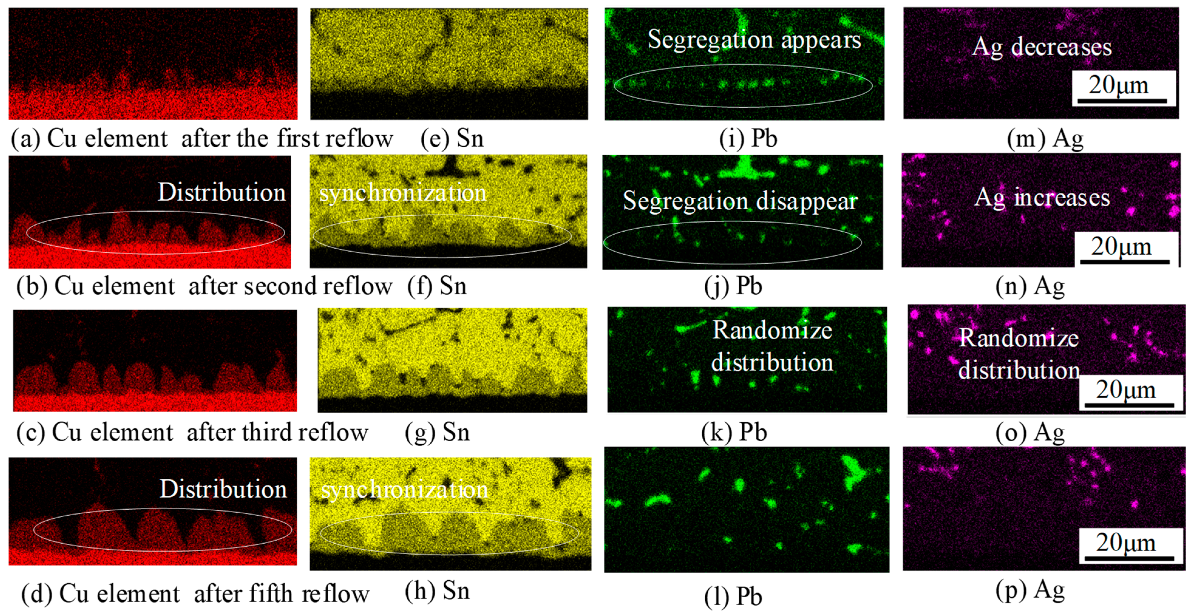
3.2. Changes in Elemental Distribution

To analyze the influence of different reflow cycles on elemental variations during liquid–solid interfacial reactions in micro-solder joints, an elemental area scan analysis was first conducted at the interface of the solder joint after a single reflow process. As shown in Figure 3b, only peaks corresponding to Cu, Sn, Ag, and Pb were detected at the interface, with no Ni observed. Figure 3c indicates that the reactive interface primarily consists of Sn (dominant) and Ag (minor) from the solder ball, Cu (dominant) from the PCB substrate, and Pb from the solder paste. A depth-resolved analysis of the reaction interface reveals the following trends: The Sn concentration increases gradually from the PCB side toward the interior of the solder ball, stabilizes at a plateau (Figure 3g,h), and exhibits fluctuations upon encountering Pb– and Ag–rich regions. The Cu concentration decreases sharply with depth, stabilizes temporarily, and eventually approaches zero within the solder matrix (Figure 3g,h). Figure 3d–f present schematic diagrams of the composite area scan compositions after multiple reflow cycles. Corresponding Figure 3i,j demonstrate that the intermetallic compound (IMC) layers formed under repeated reflow processes exhibit identical elemental variation trends, confirming cycle-independent interfacial stoichiometry.
Figure 4 delineates interfacial elemental evolution under varying reflow cycles. Comparative EDS mapping (Figure 4e–h) reveals Sn enrichment at Cu–dominant surfaces relative to PCB copper substrates, while Ag concentrations remain stable (Figure 4m–p). Notably, Cu–Sn interdiffusion initiates intermetallic compound (IMC) formation with distinct depth-dependent architectures. Primary reflow generates prismatic IMC grains. Secondary cycling induces scalloped morphologies. Tertiary processing expands diffusion zones. Fifth-cycle specimens exhibit semi-circular configurations. The Pb distribution demonstrates cycle-dependent behavior; initial reflow shows localized Pb segregation at Cu–rich interfaces (Figure 4i), critically modifying prismatic IMC growth kinetics; subsequent cycles progressively randomize Pb distribution. Advanced cycling correlates with scalloped/semi-circular IMC geometries through Pb–induced interfacial energy modification.

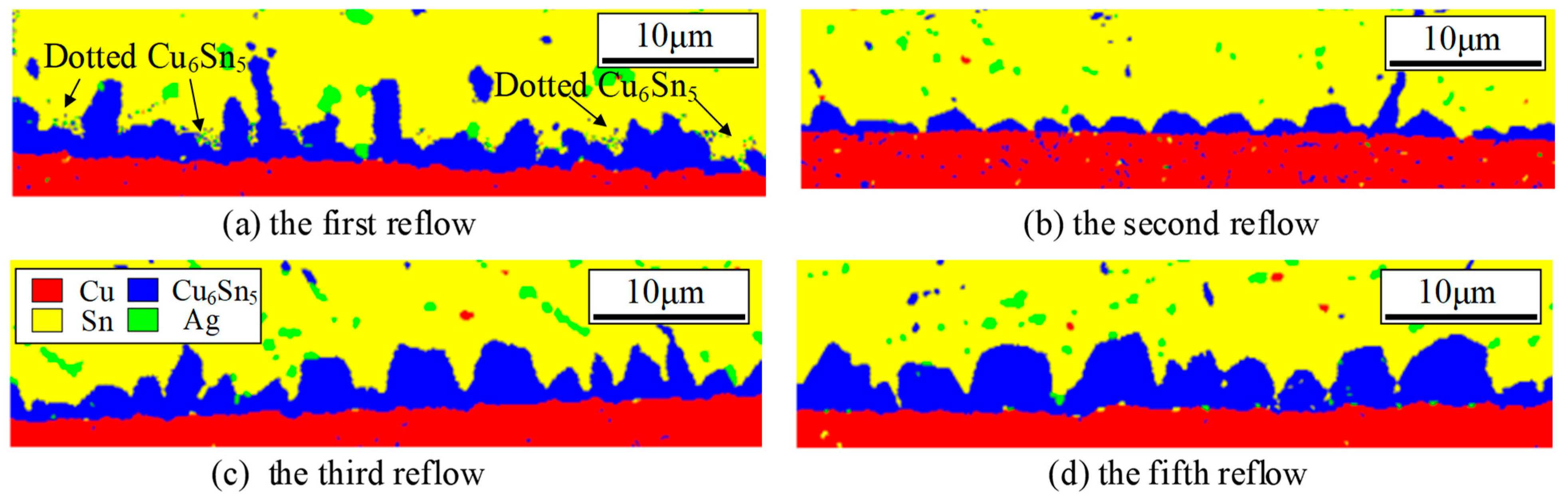
3.3. Changes in Phase Distribution

To elucidate the influence of reflow cycles on intermetallic compound (IMC) evolution during liquid–solid interfacial reactions in micro-solder joints, electron backscatter diffraction (EBSD) was employed to characterize Cu6Sn5 crystallographic features. Phase identification confirmed the exclusive formation of Cu6Sn5 compounds at interfaces (Figure 5). As shown in Figure 5a, the first reflow produced prismatic Cu6Sn5 grains with distinct growth fronts, particularly evident through surface-protruding prismatic structures near Sn–rich regions. This aligns with established coalescence mechanisms [3] where thermodynamically favored larger grains assimilate smaller neighbors under concentration gradient-driven Oswald ripening, resulting in a width increase and reduction relative to initial nucleation. Secondary reflow induced a morphological transition to planar-scalloped configurations (Figure 5b), accompanied by a 22% thickness reduction. Subsequent third reflow reversed this trend, generating thickened scallop structures with curvature radii decreasing (Figure 5c). Quintuple reflow cycles ultimately produced semi-circular Cu6Sn5 architectures, exhibiting maximum thickness accumulation through enhanced Cu–Sn interdiffusion (Figure 5d).

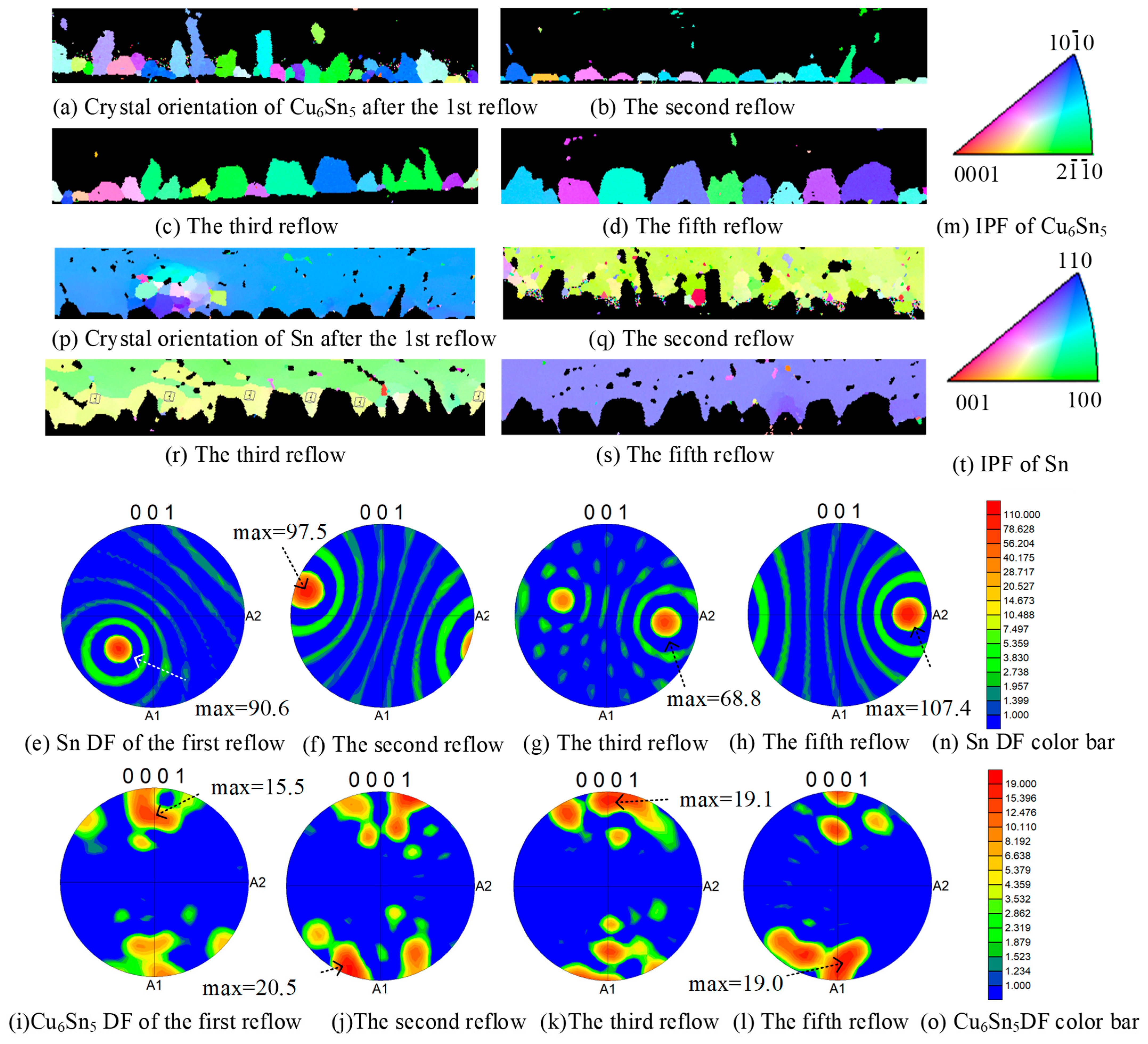
3.4. Change in Crystal Orientation

Figure 6 delineates crystallographic orientation evolution of Sn and Cu6Sn5 during liquid–solid interfacial reactions under multiple reflow cycles. Electron backscatter diffraction (EBSD) mapping (Figure 6p–s) reveals Sn’s progressive texture development, evidenced by the pole figure (PF) quantified through pole figure maxima (PFmax). Primary reflow initiates moderate Sn alignment (PFmax = 97.5), followed by secondary reflow-induced DF reduction and subsequent quintuple-cycle recovery. Cu6Sn5 exerts templating effects on Sn orientation (Figure 6r) through lattice matching mechanisms, consistent with prior reports [11,12]. Notably, Cu6Sn5 displays distinct <0001> fiber texture dominance across cycles (Figure 6i–l). Initial reflow generates stochastic orientations (PFmax = 15.5) characteristic of nucleation-controlled growth. Secondary reflow enhances preferential alignment by 32.3% (PFmax = 20.5), while tertiary and quintuple cycles exhibit moderated texture intensities (19.1 and 19.0). Multiple refluxes caused the crystals to show homogeneous growth, and the crystal orientation maximum density PFmax showed a slight decreasing trend.
Enhanced Cu6Sn5 crystallographic growth features at solder interfaces correlate with increased orientation diversity and elevated average kernel average misorientation (KAMave). Figure 7 quantifies reflow cycle effects on KAMave evolution. Primary reflow exhibits the maximum KAMave (0.68°) due to anisotropic prismatic growth (Figure 7a), with elongated grains generating high geometrically necessary dislocation (GND) densities. The maximum KAMave after the first reflow revealed distinct Pb aggregation at micro-joint interfaces (Figure 4i), exhibiting quasi-periodic distribution patterns as illustrated. Concurrently, elemental mapping confirmed active diffusion of Cu atoms from PCB pads into the solder matrix. Secondary reflow demonstrates a 46% KAMave reduction (0.37°) through stabilized planar grain structures (Figure 7b), attributed to boundary migration-induced strain relaxation. During second reflow heating, metastable prismatic Cu6Sn5 and Pb aggregates from initial reflow undergo dissolution, leaving only orientation-stabilized scallop-type Cu6Sn5 with preferred <0001> alignment (Figure 6i–l). Tertiary reflow initiates scalloped growth patterns, causing moderate KAMave resurgence (0.52°), remaining 23.5% below initial values (Figure 7c). Quintuple cycles exhibit renewed KAMave escalation (0.61°) coinciding with coarse-grained coalescence (Figure 7d). In the fifth reflow isothermal stage, progressive Cu6Sn5 grain growth creates enhanced Cu concentration gradients at adjacent grain interfaces. This drives Ostwald ripening where larger grains engulf smaller ones, leading to substantial thickness augmentation through coalescence-dominated growth. Subsequent isothermal holding promotes gradual grain coalescence with diminishing growth rates proportional to reflow cycle increments.

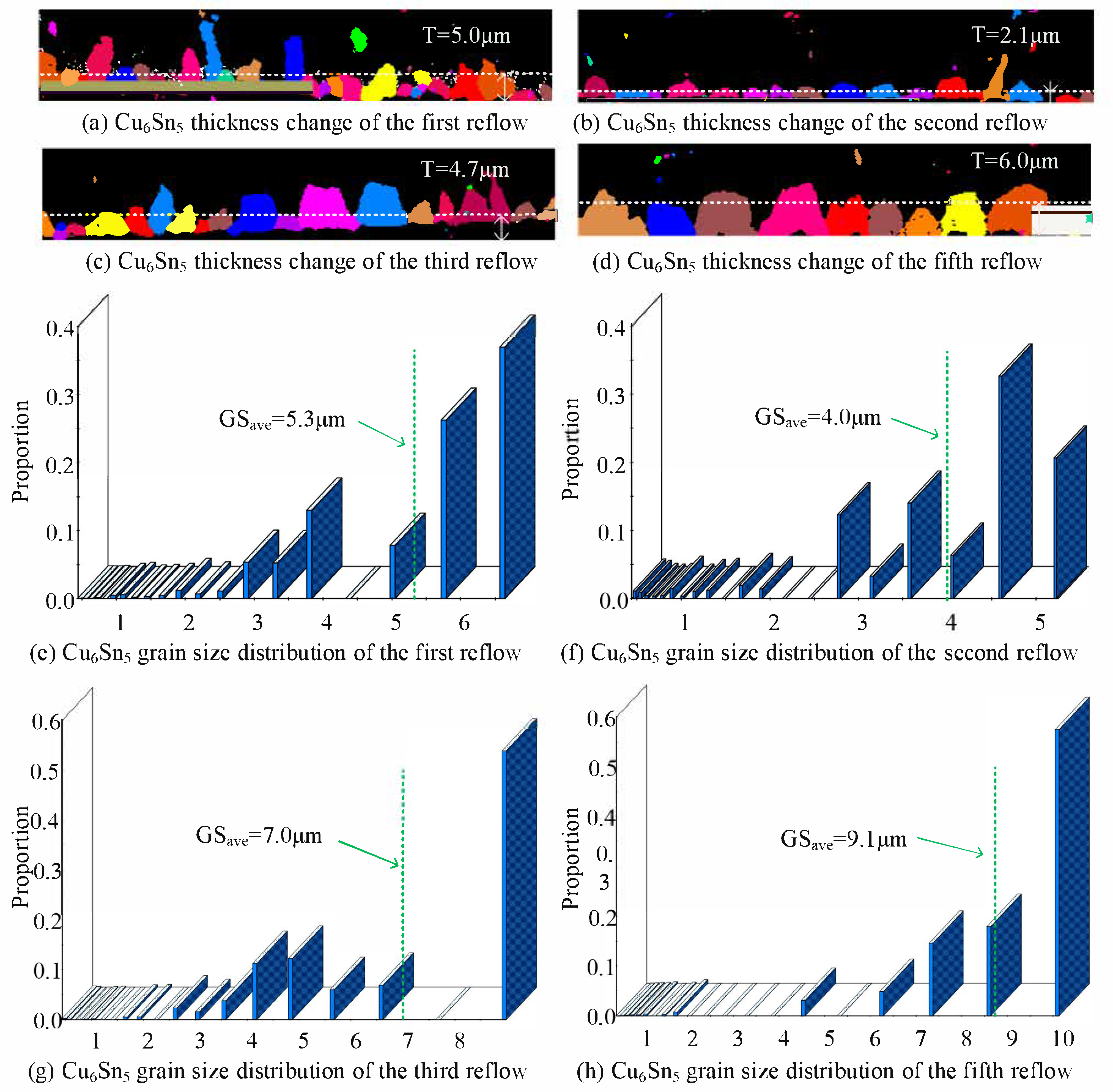
3.5. Size and Thickness Variations
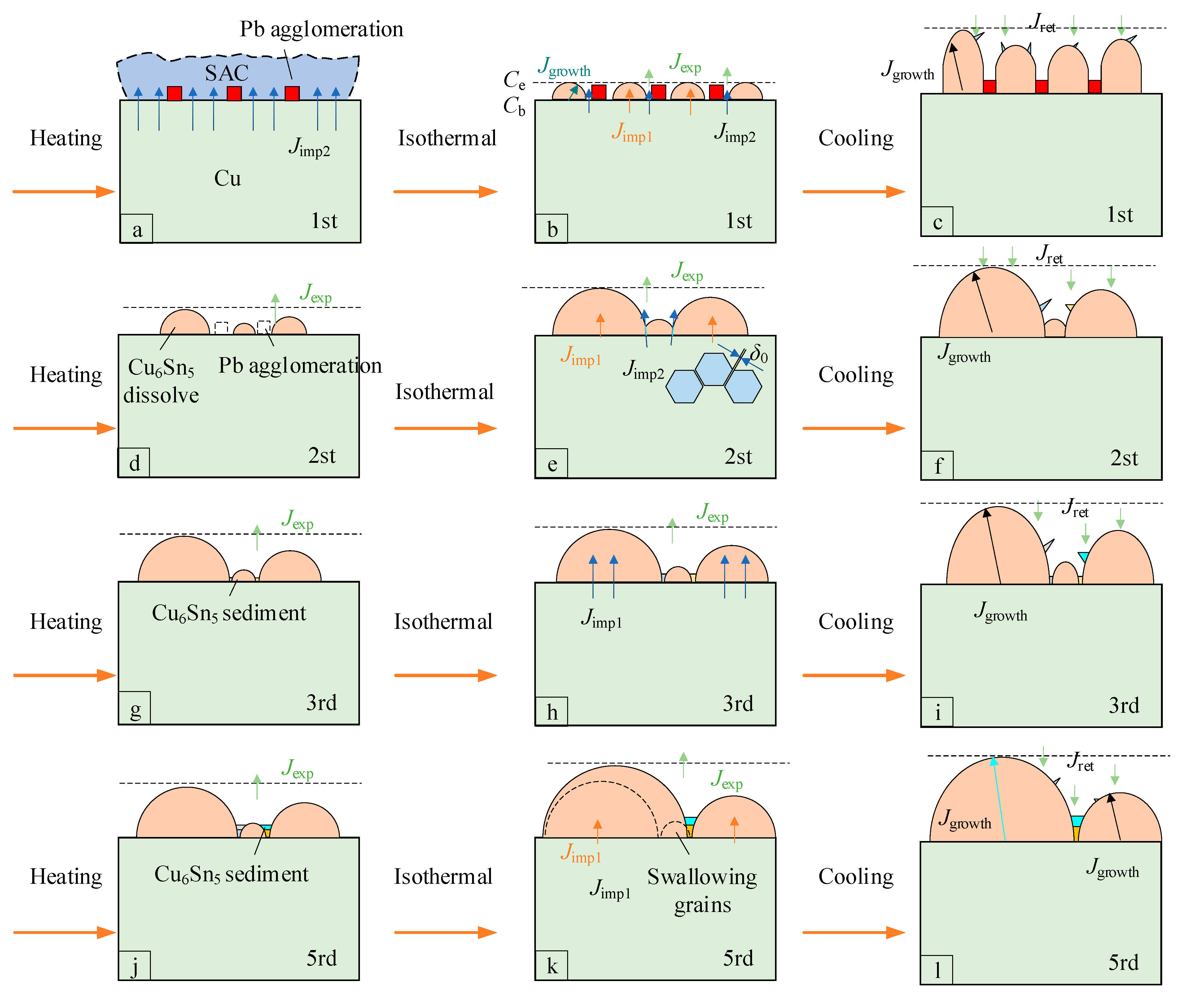
Figure 8 demonstrates the effect of multiple reflow cycles on the thickness evolution of Cu6Sn5 intermetallic compounds. Quantitative phase composition analysis of Cu6Sn5 thickness was initially performed using electron backscatter diffraction (EBSD). Within OIM analysis software, the phase boundary between Cu6Sn5 and Cu substrates served as the reference interface. Phase fraction percentages were statistically evaluated across a standardized measurement zone (width: 100 μm × height: 18 μm) along the depth direction. The average Cu6Sn5 thickness was subsequently derived by multiplying the quantified phase percentage with the total height (18 μm). Notably, this phase fraction-based metrology exhibited negligible sensitivity to specimen tilt angles due to its area-averaging measurement principle. The resultant thickness values are systematically presented in Figure 8. Figure 8e–h illustrate the grain size distribution of Cu6Sn5 crystals under varying reflow conditions. During EBSD characterization, individual grains were defined as contiguous pixel clusters meeting two crystallographic criteria: (1) adjacent pixels within a grain maintained misorientation angles below 5°, and (2) minimum grain dimensions encompassed at least two pixels along both principal axes. Grain size quantification employed the following computational approach: G S ave = i = 1 N V i × g / N , where Vi represents the total pixel count within the i-th grain, and g denotes the real-space area corresponding to a single EBSD pixel (0.09 μm2/pixel in this study).
Following the initial reflow process, the slender-growth morphology of Cu6Sn5 crystals induced a notable increase in average crystallite dimensions, attaining 5.3 μm in size (Figure 8e) and 5.0 μm in thickness (Figure 8a). The presence of distinct fine crystalline structures undergoing active growth was evident on Cu6Sn5 surfaces, exerting significant influence on the growth kinetics of interfacial intermetallic compounds (IMCs). Enhanced aspect ratios of IMC grains promoted morphological elongation, thereby amplifying the interfacial grain boundary area fraction. This microstructural evolution consequently intensified the contribution of grain boundary diffusion to IMC dimensional growth [13]. Secondary reflow processing resulted in morphological transformation of Cu6Sn5 crystals into flattened configurations, accompanied by substantial dimensional reductions to 4.0 μm in size (Figure 8f) and 2.1 μm in thickness (Figure 8b). The Cu6Sn5 phase formed during preceding low-temperature stages underwent rapid dissolution upon subsequent thermal cycling, ultimately retaining only stabilized sub-micron particles with preferential crystallographic orientations [14]. After tertiary reflow, uniform crystal growth manifested with dimensional parameters reaching 7.0 μm in size (Figure 8g) and 4.7 μm in thickness (Figure 8c), while maintaining relative grain population stability. This processing stage predominantly exhibited scallop-type Cu6Sn5 growth morphology. Progressive reflow cycling culminated in fifth-stage specimens demonstrating maximum dimensions of 9.1 μm in size (Figure 8h) and 6.0 μm in (Figure 8d) thickness, concurrent with substantial grain population reduction. Conspicuous grain coalescence phenomena emerged during fifth reflow, consistent with the literature [15] reporting pronounced coalescence and growth mechanisms during dwell phases of multi-reflow processes. Gradual inter-granular coalescence of Cu6Sn5 crystals occurs during thermal equilibration, with concomitant decay in growth kinetics as reflow iterations increase.

4. Discussion

The growth behavior of interfacial intermetallic compounds (IMCs) during multi-stage hybrid soldering processes results from synergistic interactions among three critical thermal phases: heating ramp-up, isothermal dwell, and controlled cooling. This multi-mechanism process is governed by competing transport phenomena including grain boundary diffusion, bulk lattice diffusion, interfacial precipitation, and dissolution-redistribution mechanisms. Notably, IMC grain morphology exerts significant influence on solder joint interfacial reaction kinetics. During primary reflow heating, incomplete dissolution occurred in 120 μm thick Sn63Pb37 solder paste (Indium Corporation) deposited on bonding pads. Microstructural analysis revealed distinct Pb aggregation at micro-joint interfaces (Figure 4i), exhibiting quasi-periodic distribution patterns as illustrated in Figure 9a. Concurrently, elemental mapping confirmed active diffusion of Cu atoms from PCB pads into the solder matrix. The growth rate of Cu6Sn5 [16] is as follows:
d l d t = J imp 1 + J imp 2 J exp C η ρ η
where Jimp1 represents the Cu atomic flux entering the interfacial region through Cu6Sn5 grains; Jimp2 denotes the Cu atomic flux entering through intergranular gaps of Cu6Sn5; and Jexp signifies the Cu flux from the interfacial region into the bulk solder. Cη indicates the Cu mass fraction in Cu6Sn5, while ρη corresponds to the densities of the intermetallic compound (IMCs) and liquid solder phase, respectively. During isothermal dwell, reduced grain dimensions and expanded intergranular spacing render Cu6Sn5 growth primarily dependent on gap diffusion between grains as demonstrated in Figure 9b. The intergranular Cu flux Jimp2 is formulated as follows [2]:
J imp 2 = D l ρ l C b C e l 1 + 3 l 2 δ
where Dl is the diffusion coefficient of Cu atoms in the liquid solder; ρl represents the density of Cu atoms in the solder phase; Cb denotes the equilibrium Cu concentration in the liquid solder at the grain boundary bottom contacting the substrate; Ce indicates the equilibrium Cu concentration in the liquid solder at the grain boundary top interfacing with the IMCs; l corresponds to both the average thickness of interfacial Cu6Sn5 and the radius of Cu6Sn5 grains; and δ specifies the intergranular distance between adjacent Cu6Sn5 grains. The Cu atomic flux Jexp [13] through interfacial Cu6Sn5 gaps into the boundary region is expressed as follows:
J exp = K d ρ l C s e K d t / l 0 l
where Kd denotes the diffusion rate constant of Cu atoms into the liquid solder; Cs represents the saturated Cu concentration in the liquid solder at soldering temperature; l0 corresponds to the height of the solder body; and t indicates the reaction time. During the initial stage of first reflow, the smaller Cu6Sn5 grain size l and larger intergranular distance δ between adjacent Cu6Sn5 grains result in a significant increase in Jimp2. The intermetallic compounds (IMCs) exhibit maximum growth rate during isothermal holding compared to multiple reflow cycles, preferentially nucleating along the [0001] crystallographic orientation of Cu6Sn5 (Figure 6i–l). Subsequent cooling reduces Cu solubility at the interface due to decreasing temperature, promoting additional Cu6Sn5 formation. This process is enhanced by localized Pb segregation at the interface (Figure 4i) and elevated interfacial Cu concentration. As shown in Figure 9c, air-cooling induces a distinct lamellar distribution of Cu6Sn5 grains, with observable dot-shaped precipitates near Sn–rich regions and prismatic Cu6Sn5 grains demonstrating active growth characteristics (Figure 6a). The literature [2] demonstrates that cooling/heating cycles primarily influence Cu6Sn5 vertical height, while isothermal holding governs lateral width and population density. During second reflow heating, metastable prismatic Cu6Sn5 and Pb aggregates from initial reflow undergo dissolution, leaving only orientation-stabilized scallop-type Cu6Sn5 with preferred [0001] alignment (Figure 9d). Progressive isothermal holding promotes gradual coarsening of adjacent Cu6Sn5 grains, reducing intergranular spacing to critical boundary distance δ0 (Figure 9e). Small-sized Cu6Sn5 formed during secondary reflow air-cooling (Figure 9f) subsequently dissolve and accumulate at grain boundaries during third reflow heating (Figure 9g), effectively blocking Cu grain boundary diffusion during thermal aging (Figure 9h). This transition shifts the dominant diffusion mechanism from grain boundary transport to bulk lattice diffusion through Cu6Sn5 crystals. The corresponding bulk diffusion flux Jimp1 [15] is expressed as follows:
J imp 1 = D η S a ρ η 1 C η l
During the triple isothermal process, interfacial Cu diffusion flux primarily occurs via bulk diffusion. The growth thickness l of Cu6Sn5 follows a t1/2 temporal dependence. With increasing reflow cycle numbers, the temporal growth exponent for Cu6Sn5 formation during isothermal holding transitions from 1/3 (observed in secondary isothermal process) to 1/2, accompanied by reduced growth kinetics. Surface Cu concentration in crystalline regions decreases concurrently, inducing overall crystal coarsening. In the fifth reflow isothermal stage, progressive Cu6Sn5 grain growth creates enhanced Cu concentration gradients at adjacent grain interfaces. This drives Ostwald ripening where larger grains engulf smaller ones (Figure 9k), leading to substantial thickness augmentation through coalescence-dominated growth. Subsequent isothermal holding promotes gradual grain coalescence with diminishing growth rates proportional to reflow cycle increments. The Cu6Sn5 growth rate exhibits systematic attenuation as reflow repetitions increase.

5. Conclusions

This study investigates the interfacial intermetallic compound (IMC) growth mechanisms and kinetics in Pb–free/Pb–containing hybrid micro-solder joints under multiple reflow cycles. Key findings are summarized as follows:
(1)
The interfacial IMCs in hybrid solder joints predominantly consist of Cu6Sn5 grains. With increasing reflow cycles, Pb distribution transitions from clustered to random dispersion patterns, accompanied by the progressive transformation of prismatic Cu6Sn5 into scallop-shaped and semicircular configurations.
(2)
Cu6Sn5 grains exhibit pronounced preferential orientation along the horizontal crystallographic direction across all reflow cycles, with this orientation influencing Sn crystal alignment.
(3)
Quantitative EBSD analysis reveals microstructural evolution. The first reflow elongates Cu6Sn5 grains, exhibiting high aspect ratios, with observable fine crystalline protrusions indicating active growth, and the second reflow reduces both dimensions significantly. Scallop-type Cu6Sn5 of the third reflow demonstrates uniform growth with a stable grain population, and coarsening dominates after the fifth reflow, accompanied by pronounced grain coalescence.

Author Contributions

Conceptualization, Y.B.; methodology, Q.C.; software, L.F.; validation, L.F., Z.Z. and C.Z.; formal analysis, Q.Z.; investigation, Y.B.; data curation, Q.Z.; writing—original draft preparation, X.H.; writing—review and editing, Y.W.; visualization, C.Z.; supervision, X.H.; project administration, X.H.; funding acquisition, Y.W. All authors have read and agreed to the published version of the manuscript.

Funding

This research was funded by [National Natural Science Foundation of China] grant number [52405507], [Fundamental Research Program of Shanxi Province] grant number [202203021212233], [Fundamental Research Program of Shanxi Province] grant number [202203021222123], [Research Project Supported by Shanxi Scholarship Council of China] grant number [2021-048].

Data Availability Statement

The original contributions presented in this study are included in the article. Further inquiries can be directed to the corresponding author(s).

Conflicts of Interest

The authors declare no conflict of interest.

References

  1. Le, F.; Lee, S.W.; Zhang, Q. 3D chip stacking with through-silicon-vias (TSVs) for vertical interconnect and underfill dispensing. J. Micromech. Microeng. 2017, 27, 045012. [Google Scholar] [CrossRef]
  2. Ma, H.R.; Kunwar, A.; Shang, S.Y.; Jiang, C.R.; Wang, Y.P.; Ma, H.T.; Zhao, N. Evolution behavior and growth kinetics of intermetallic compounds at Sn/Cu interface during multiple reflows. Intermetallics 2018, 96, 1–12. [Google Scholar] [CrossRef]
  3. Qu, L.; Zhao, N.; Zhao, H.; Huang, M.; Ma, H. In situ study of the real-time growth behavior of Cu6Sn5 at the Sn/Cu interface during the soldering reaction. Scr. Mater. 2014, 72, 43–46. [Google Scholar] [CrossRef]
  4. Park, M.S.; Arróyave, R. Early stages of intermetallic compound formation and growth during lead-free soldering. Acta Mater. 2010, 58, 4900–4910. [Google Scholar] [CrossRef]
  5. Chen, H.; Tsai, Y.-L.; Chang, Y.-T.; Wu, A.T. Effect of massive spalling on mechanical strength of solder joints in Pb-free solder reflowed on Co-based surface finishes. J. Alloys Compd. 2016, 671, 100–108. [Google Scholar] [CrossRef]
  6. Haseeb, A.S.; Arafat, M.M.; Johan, M.R. Stability of molybdenum nanoparticles in Sn-3.8Ag-0.7Cu solder during multiple reflow and their influence on interfacial intermetallic compounds. Mater. Charact. 2012, 64, 27–35. [Google Scholar] [CrossRef]
  7. Ha, S.S.; Jang, J.K. Effect of multiple reflows on interfacial reaction and shear strength ofSn-Ag electroplated solder bumps for fip chip package. Microelectron. Eng. 2010, 87, 517–521. [Google Scholar] [CrossRef]
  8. Noh, B.I.; Koo, J.M.; Kim, J.W.; Kim, D.G.; Nam, J.D.; Joo, J.; Jung, S.B. Effects of number of reflows on the mechanical andelectrical properties of BGA package. Intermetallics 2006, 14, 1375–1378. [Google Scholar] [CrossRef]
  9. Yao, P.; Liu, P.; Liu, J. Effects of multiple reflows on intermetallic morphology and shear strength of Sn Ag Cu-xNi composite solder joints on electrolytic Ni/Au metalized substrate. J. Alloys Compd. 2008, 462, 73–79. [Google Scholar] [CrossRef]
  10. Huebner, H.; Penka, S.; Barchmann, B.; Eigner, M.; Gruber, W.; Nobis, M.; Janka, S.; Kristen, G.; Schneegans, M. Microcontacts with sub-30um pitch for 3D chip-on-chip integration. Microelectron. Eng. 2006, 83, 2155–2162. [Google Scholar] [CrossRef]
  11. Darbandi, P.; Bieler, T.R.; Pourboghrat, F.; Lee, T.-K. The effect of cooling rate on grainorientation and misorientation microstructure of SAC105 solder joints before and after impact droptests. J. Electron. Mater. 2014, 43, 2521–2529. [Google Scholar] [CrossRef]
  12. Chang, Z.Y.; Zhao, N.; Wu, C. Effects of cooling rate and joint size on Sn grain features inCu/Sn-3.5Ag/Cu solder joints. Materialia 2020, 14, 100929. [Google Scholar] [CrossRef]
  13. Ma, H.; Kunwar, A.; Huang, R.; Chen, J.; Wang, Y.; Zhao, N.; Ma, H. Size effect on lMC growth induced by Cu concentration gradient and pinning of Ag3Sn particles during multiple reflows. Intermetallics 2017, 90, 90–96. [Google Scholar] [CrossRef]
  14. Huang, M.; Yang, F.; Zhao, N.; Zhang, Z. In situ study on dissolution and growth mechanism of interfacial Cu6Sn5 in wetting reaction. Mater. Lett. 2015, 139, 42–45. [Google Scholar] [CrossRef]
  15. Ma, H.; Ma, H.; Kunwar, A.; Shang, S.; Wang, Y.; Chen, J.; Huang, M.; Zhao, N. Effect of initial Cu concentration on the lMC size and grain aspect ratio in Sn-xCu solders during multiple reflows. J. Mater. Sci. Mater. Electron. 2018, 29, 602–613. [Google Scholar] [CrossRef]
  16. Li, J.; Mannan, S.; Clode, M.; Whalley, D.; Hutt, D. Interfacial reactions between molten Sn-Bi-X soldersand Cu substrates for liquid solder interconnects. Acta Vaterialia 2006, 54, 2907–2922. [Google Scholar] [CrossRef]
Figure 1. Experimental process diagram.
Crystals 15 00516 g001
Figure 2. Gradient distribution of IMCs with different reflux times.
Crystals 15 00516 g002
Figure 3. Elements line scan results at the interface of micro solder joints.
Crystals 15 00516 g003
Figure 4. Elements line scan results at the interface of micro-solder joints.
Crystals 15 00516 g004
Figure 5. Phase analysis of IMCs with different reflux times.
Crystals 15 00516 g005
Figure 6. Crystal orientation analysis of IMCs with different reflux times.
Crystals 15 00516 g006
Figure 7. KAM distribution of IMCs with different reflux times.
Crystals 15 00516 g007
Figure 8. Size and thickness distribution of IMCs with different reflux times.
Crystals 15 00516 g008
Figure 9. IMC growth model at SAC solder ball and Cu interface.
Crystals 15 00516 g009
Disclaimer/Publisher’s Note: The statements, opinions and data contained in all publications are solely those of the individual author(s) and contributor(s) and not of MDPI and/or the editor(s). MDPI and/or the editor(s) disclaim responsibility for any injury to people or property resulting from any ideas, methods, instructions or products referred to in the content.

