Abstract
Microwave Plasma Chemical Vapor Deposition (MPCVD) plays a crucial role in the growth of high-quality diamonds. However, during the MPCVD process, residues such as polycrystalline diamond, and graphite often adhere to the high-temperature growth substrate surfaces, potentially degrading diamond growth quality. To effectively remove these contaminants and improve the quality of diamond growth, this study employed an 800 kHz femtosecond laser to clean growth substrates with residual deposits. We assessed the effects of multiple cleaning cycles on residue removal from the Foundation Trench Region (FTR) and Inwall Region (IR) and on substrate quality. The results indicate that multiple scans at a laser power of 2.38 W, a repetition rate of 800 kHz, a scanning speed of 1800 mm/s, and a scan spacing of 10 μm significantly removed residues, reduced substrate surface roughness, and restored substrate cleanliness. This approach enhances the quality and efficiency of diamond growth via MPCVD. The application of high-repetition-rate femtosecond laser cleaning techniques for growth substrates significantly improves the quality of regenerated diamond films, providing crucial support for the preparation of high-quality diamond materials.
1. Introduction
MPCVD (Microwave Plasma Chemical Vapor Deposition) is widely utilized in the preparation of large-area, high-quality single-crystal diamonds due to advantages such as high electron density in the plasma, the absence of electrode contamination, and superior diamond growth quality [1,2]. However, during the MPCVD growth process, interactions between the high-temperature substrate and raw materials like H2 and CH4 often result in the deposition of residues on the substrate surface [3,4]. These residues include incompletely grown polycrystalline diamonds, graphite crystals, and amorphous carbon contaminants [5,6]. The residual material at the edge of the substrate will lead to the rapid growth of polycrystalline materials at these locations in the subsequent MPCVD stage [7,8]. This rapid growth can cause a significant temperature drop around the seed crystal during growth, thereby adversely affecting crystal growth quality, as illustrated in Figure 1. Figure 1a shows diamonds grown on a substrate without surface residues; they have high-quality growth with uniform crystal morphology. In contrast, Figure 1b shows diamonds grown on a substrate with surface residues, resulting in poorer quality growth with uneven crystal morphology. Clearly, the removal of surface residues from the growth substrate is crucial for achieving high-quality MPCVD diamond growth.
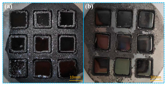
Figure 1.
The effect of residues of growth substrate on MPCVD diamond growth. (a) Diamond grown on a clean growth substrate. (b) Diamond grown on a growth substrate with residues.
Therefore, to ensure the high-quality growth of single-crystal diamonds, it is essential to effectively clean the surface of the growth substrate. However, due to the strong adhesion between the residues and the substrate surface, conventional methods such as mechanical cleaning, chemical cleaning, and ion beam cleaning often fail to achieve the desired cleaning effect. In contrast, laser cleaning promises non-contact and high efficiency, and it has been widely used in die cleaning. It not only extends the lifespan of the growth substrate but also provides a cleaner surface for the high-quality growth of single-crystal diamonds, significantly enhancing the quality and efficiency of diamond growth [9,10]. In a previous study, Jia et al. [11] studied the removal of rubber contaminants from a chrome-plated die with slots using an acousto-optic Q-switched Nd:YAG nanosecond pulsed laser with an average power of 100 W. Using a positive defocused laser, the single pulse energy density was 0.97 J/cm2, and argon gas was added to achieve the efficient cleaning of the mold in a single scan. Wang et al. [12] studied the 1064 nm Nd:YAG pulsed laser cleaning of a tire die. The cleaning threshold of the rubber was 18.6 J/cm2, and the substrate damage threshold was 22.0 J/cm2. It can be seen that a nanosecond laser can clean a mold, but the thermal effect is serious and can easily damage the substrate and reduce the strength of the substrate. Femtosecond laser ablation, with its advantages of non-contact, high precision, high efficiency, and cold processing characteristics, is widely used in the surface treatment and cleaning of various materials [13,14]. Rivas et al. [15] used a femtosecond Ti–sapphire laser to clean granite at its fundamental wavelength (790 nm) and subharmonic level (395 nm). The extremely small heat load on the substrate caused by ultrashort laser pulse irradiation minimized any side effects caused by heat conduction (carbonization, cracking, chemical modification, etc.). It can be seen that a femtosecond laser has no thermal effect during cleaning but instead uses a thermal expansion effect and elastic force to fragment, vaporize, and remove the deposits, achieving the purpose of efficient cleaning [16,17].
After femtosecond laser cleaning, the mold surface often remains rough, which is detrimental to the growth of MPCVD diamonds. To address this issue, it is necessary to introduce a slight thermal effect to reduce the surface roughness of the mold post-cleaning. There are generally two methods to achieve this. The first method involves using a femtosecond–nanosecond composite laser. By introducing the thermal effects of the nanosecond laser, the surface roughness of the mold after cleaning can be adjusted [18]. However, this composite hybrid laser system is complex and expensive. The second method is to use a high-repetition-rate femtosecond laser. This approach effectively introduces the necessary thermal effect to smooth the surface without the complexity and cost associated with hybrid laser systems. Consequently, using a high-repetition-rate laser is a more practical and economical solution for reducing mold surface roughness after femtosecond laser cleaning. Shin et al. [19] demonstrated that using low flux and applying high repetition pulse widths can reduce thermal damage caused by heat accumulation while ensuring high productivity. Therefore, we can use an 800 kHz high-repetition-rate femtosecond laser to clean the substrate, which can reduce thermal effects and avoid excessive substrate roughness caused by complete cool-cleaning. Since optimizing these parameters can improve cleaning speed and efficiency, adjusting the appropriate laser cleaning conditions is crucial to obtain the best results for substrate surfaces with different types of contaminants [20]. Chen et al. [21] conducted a single-pulse separation ablation experiment on a single-crystal diamond using femtosecond lasers of different powers. The results showed that the femtosecond laser single-pulse ablation threshold of single-crystal diamonds is 8.80 J/cm2. Therefore, setting an appropriate high-repetition-rate femtosecond laser power can remove MPCVD residues.
Based on the analysis above, this study used an 800 kHz femtosecond laser with an average power of 2.38 W to clean the MPCVD diamond growth substrate. We evaluated the cleaning quality by analyzing the morphology before and after processing and assessed the feasibility and advantages of 800 kHz femtosecond laser cleaning technology in improving the surface quality of growth substrates and the quality of diamond single-crystal growth.
2. Materials and Methods
2.1. Sample Preparation
Figure 2a shows a schematic of a molybdenum alloy diamond MPCVD growth substrate with a radius of 35 mm and a height of 6 mm. In Figure 2b, it is evident that MPCVD residues deposited on the FTR (Foundation Trench Region) accumulate on the molybdenum alloy surface in the form of aggregated granules, obscuring the molybdenum substrate. As shown in Figure 2d, residues deposited on the IR (Inwall Region) exhibit a thick-layered structure with a thickness ranging from 30 μm to 50 μm. Therefore, the MPCVD particles deposited inside the trench differ from common uniform contaminants. The substrate of the growth base is a molybdenum alloy, as indicated in Table 1.
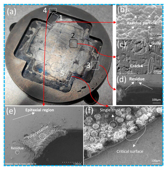
Figure 2.
Schematic diagram of the MPCVD growth substrate and various regions: (a) Schematic diagram of the MPCVD growth substrate. (b) Residue particles on FTR. (c) FTR surface. (d) Residue on IR. (e) Epitaxial layer surface. (f) Residue and FTR interface.

Table 1.
Chemical composition of molybdenum alloy.
Before laser cleaning, the MPCVD growth substrate surface was carefully wiped with alcohol. Figure 2c reveals cracks that intersect each other in a grid-like pattern, with numerous irregularly shaped grooves appearing on the FTR surface. Figure 2b,f illustrate residual materials (comprising crystalline graphite, polycrystalline diamond, etc.) remaining on the planar area during the laser cleaning of MPCVD processes. Additionally, as shown in Figure 2d, residue distribution on the IR surface is uneven, with not all areas of the IR surface exhibiting residues. The interface between MPCVD residues and the growth substrate is depicted in Figure 2f, showing a residual layer thickness of approximately 40 μm.
2.2. Laser Cleaning
A schematic diagram of the femtosecond laser cleaning system is shown in Figure 3. The femtosecond laser used is a femto laser produced by Huaray Laser (Wuhan, China), with a pulse width of 250 fs, a maximum single pulse energy of 50 μJ, a maximum average power of 40 W, a repetition rate of 800 kHz, a beam quality M2 less than 1.3, a beam divergence angle less than 0.5 mrad, linear polarization, and a laser wavelength of 1035 nm. After focusing through an F-theta lens, the spot diameter is 15 μm. The laser scanning area is 10 mm × 10 mm. Depending on the cleaning position, the MPCVD growth substrate is placed either flat (for bottom-surface cleaning) or at a 45° angle (for side-surface cleaning). After completing the system study, the samples were cleaned with multiple sets of parameters. By evaluating the degree of surface damage on the molybdenum alloy substrate cleaned under different parameters, suitable laser parameters were determined, as shown in Table 2.
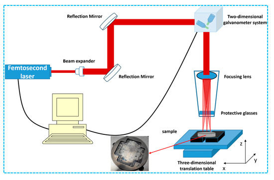
Figure 3.
Schematic diagram of femtosecond laser cleaning system.
Table 2.
Laser parameters.
2.3. Characterization Methods
In this study, a Hitachi tabletop scanning electron microscope (SEM), model TM4000Plus (Hitachi, Ltd., Tokyo, Japan), equipped with an energy dispersive spectrometer (EDS), was used for SEM characterization and an elemental analysis of the samples. Additionally, an Olympus confocal microscope, model OLS-5100 (Olympus, Ltd., Tokyo, Japan), and a Horiba automated micro-confocal Raman spectrometer, model XploRA PLUS (Horiba, Kyoto, Japan), were utilized for roughness measurement and Raman analysis of the samples, respectively.
3. Results and Discussion
3.1. MPCVD Residual Substance Composition Analysis
The residuals were analyzed using EDS elemental spectroscopy and Raman spectroscopy before cleaning. EDS spectroscopy was employed to map the elemental distribution of the residuals, while Raman spectroscopy recorded the Raman scattering signals of the residuals across different wavenumber ranges. Figure 4a,b show elemental maps of the residuals and the FTR interface area from Figure 2f. These maps indicate that the residual areas primarily consist of carbon, with the minimal presence of other elements. Figure 5a presents the Raman spectrum of pure diamond, serving as reference data. The characteristic Raman peak for diamond is observed at 1332 cm−1. Analysis of this Raman peak allows for the identification of the material as diamond, graphite, or hexagonal carbon. Peak shifts can indicate internal stress, and peak broadening can suggest structural defects, thereby helping assess the quality of the diamond. The relative intensity of the characteristic peak can also be used to estimate the thickness of the diamond film. As shown in Figure 5a, the Raman spectrum fitting reveals no graphite peak in the spectrum of the original pure diamond material, but a distinct characteristic peak is observed at 1332 cm−1, confirming the diamond’s characteristic Raman peak. Figure 5b shows the fitted Raman spectrum of the residuals, displaying a prominent peak at 1304 cm−1, close to the 1332 cm−1 peak of pure diamond. The presence of the 1304 cm−1 peak in the residual spectrum, similar to the 1354 cm−1 peak in pure diamond, indicates that a significant amount of diamond exists within the residuals. However, additional peaks, such as the graphite peak, suggest that the residuals primarily consist of single-crystal diamonds with small amounts of graphite and other substances [22].
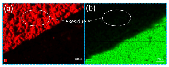
Figure 4.
EDS map of the (a) residue and (b) FTR interface, respectively.
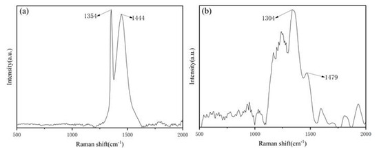
Figure 5.
Raman spectrum of (a) pure diamond single crystals and (b) residue on the substrate.
3.2. Laser Cleaning of Residual Particles on FTR
The EDS results for the contaminants on the FTR and IR surfaces before laser cleaning are shown in Table 3 (a). Before cleaning, the total carbon content reached 98.62 wt%, while the molybdenum content was 1.38 wt%.
Table 3.
Average composition of the growth substrate surface before and after cleaning (in wt.%).
As shown in Figure 2a, the presence of single-crystal diamond residues is clearly visible on the surface of the base groove and its inner walls before cleaning. These residues not only affect the smoothness of the base groove but also adversely impact the subsequent single-crystal diamond growth process.
Figure 6b shows the experimental results of cleaning multiple scans of the laser parameters in parameter model I (Table 2) after testing. As can be seen from Figure 6b, there is no obvious damage to the substrate, and the cleaning results are acceptable. After cleaning the single-crystal diamond particles on the FTR using laser parameter II, a clear and smooth surface can be observed with no damage to the substrate. This indicates that the optimal laser parameters for removing single-crystal diamond particles are a laser power of 2.38 W, a repetition rate of 800 kHz, and a scanning speed of 1800 mm/s, which cause minimal damage to the molybdenum substrate. The SEM results in Figure 6a,b show that the surface smoothness of the base groove was very low before cleaning due to the accumulation of single-crystal diamond residues. After cleaning, the surface smoothness of the base groove improved significantly, with residues effectively removed and minimal damage observed. There was no obvious ablation or formation of cracks, and the substrate remained undamaged. This demonstrates that femtosecond laser cleaning technology can thoroughly remove single-crystal diamond residues without damaging the base surface, thereby enhancing the quality and reusability of the base.
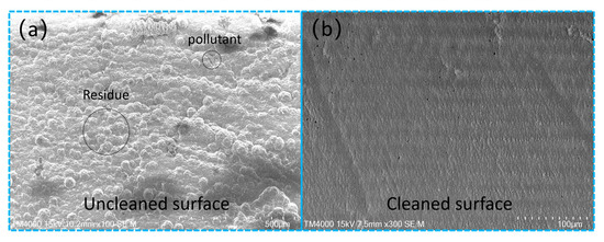
Figure 6.
SEM images of residues on the FTR surface (a) before and (b) after cleaning.
The EDS results before cleaning in Table 3 (a) and Figure 7a show that the carbon (C) content was as high as 98.62 wt%, with a small amount of molybdenum (Mo) content at 1.38 wt%. Combined with the SEM results in Figure 6a, this indicates that the residues mainly consisted of single-crystal diamonds. To avoid adverse effects on the diamond single-crystal growth and ensure the reuse of the growth base, ultrafast laser cleaning was performed. After cleaning, we found that the single-crystal diamond residues were effectively removed, and the chemical composition of the base surface remained largely unchanged. As shown by the EDS results in Table 3 (c) and (d) and Figure 7c, post-cleaning, the Mo content reached 86.24 wt%, while the C, O, and S contents were 0 wt%, 8.94 wt%, and 4.82 wt%, respectively. Compared to the pre-cleaning state, the Mo elemental proportion significantly increased, and the O elemental proportion significantly decreased, indicating the presence of other oxides or contaminants on the FTR surface before cleaning. The S elemental content remained essentially unchanged. The single-crystal diamond particle residues and oxides on the FTR surface were effectively removed, demonstrating that the femtosecond laser cleaning process has a high non-destructive effect on the base surface’s chemical composition, helping to preserve the base’s original performance. After 800 kHz femtosecond laser cleaning, the groove surface achieved a satisfactory cleaning effect.
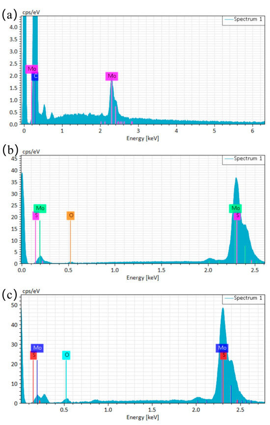
Figure 7.
EDS results: (a) residue part before cleaning; (b) molybdenum substrate (no residue diamonds exist); (c) molybdenum substrate with residue after cleaning.
Figure 8b,c show a comparison of the surface roughness results for the groove surface before and after cleaning, measured by a confocal microscope. Sa represents the average roughness of the area, which avoids skewed results due to the influence of the network of cracks and grooves on the groove surface. As shown in Figure 8a, the surface roughness was measured in four different areas of the same size on the sample, and the average value was calculated to obtain an accurate roughness measurement. According to Table 4 (a) and (b) and Figure 8b,c, it is evident that, before cleaning, the substrate surface morphology exhibited considerable fluctuations with a high roughness of about 6.557 μm. This high roughness could negatively impact the quality and surface morphology of the single-crystal diamond growth. After cleaning, the surface fluctuations were reduced, and the roughness decreased to about 5.231 μm. During the femtosecond laser cleaning process, as the surface residues were removed, the substrate’s roughness continued to decrease, effectively polishing the surface and improving its quality. This improvement in surface quality promotes the regrowth of single-crystal diamonds. Therefore, femtosecond laser cleaning technology provides an efficient and reliable method for cleaning diamond single-crystal growth substrates, with the potential to advance and be applied in related fields.
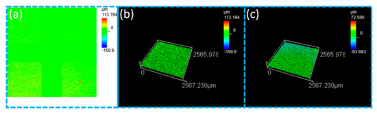
Figure 8.
Confocal microscopy roughness results before and after cleaning: (a) Ra area selection; (b) substrate roughness before cleaning; (c) substrate roughness after cleaning.
Table 4.
Surface roughness results—molybdenum base groove base surface.
During the experiments, noticeable black smoke was observed during the laser cleaning process, indicating a more complex removal mechanism than simple vaporization. In instances where the cleaning was incomplete, some areas of the MPCVD residues would break off, revealing a clean substrate underneath. This suggests that the acoustic waves generated during the laser cleaning process can exert elastic forces to remove the residues. Analyzing the laser cleaning of single-crystal diamond particles on the FTR indicates that thermoelastic expansion can serve as an additional cleaning mechanism for layered MPCVD residues. This phenomenon involves the laser-induced rapid heating and subsequent expansion of the material, generating mechanical stress that assists in dislodging the residues from the substrate. In summary, the combined effects of vaporization and thermoelastic expansion contribute to the effective removal of MPCVD residues during femtosecond laser cleaning. This dual mechanism ensures a thorough cleaning process, maintaining the integrity and cleanliness of the substrate, thereby enhancing the quality of subsequent single-crystal diamond growth.
3.3. Laser Cleaning of IR Residues
As shown in Figure 2a, the MPCVD residues on the FTR are relatively easy to clean. However, as illustrated in Figure 9a,b, single-crystal diamonds on the FTR tend to grow and extend onto the IR, even reaching the groove area. If the residues on the IR are not cleaned, it can adversely affect the quality of subsequent single-crystal diamond growth. Therefore, it is essential to use laser cleaning to remove the residues on the IR. During the laser cleaning process for IR residues, the same laser parameters are employed. However, because the IR cannot be laid flat for laser focusing, a special IR processing substrate is used to incline the sample, enabling the laser to clean the inclined surface of the IR, as shown in Figure 9d. The vertical distance between the upper and lower surfaces of the inclined IR is ±1 mm. The Rayleigh length of the laser processing system used in this study is 0.7 mm. Due to the similar magnitude of positive and negative defocusing, they exhibit comparable laser energy density and processing capabilities, resulting in similar cleaning outcomes [23]. Therefore, the laser focus is positioned at the midpoint of the IR, and this focusing method is employed to clean the residues on the IR. During the laser cleaning process, the laser first irradiates the FTR and then continues to act on the inclined surface of the IR. This process is repeated multiple times until the surface is completely clean. As shown in Figure 9c, after cleaning, the single-crystal diamond residues on the IR surface are effectively removed, leaving a relatively smooth surface. This outcome is comparable to the cleaning effect achieved on the FTR, indicating that the inclined focusing method is suitable for removing residues from the inner wall of the groove using femtosecond laser cleaning, achieving the desired cleaning effect. As depicted in Figure 2a, the IR has more extensive areas. Compared to cleaning residues on the FTR, cleaning residues on the IR is more challenging. However, by employing this rapid positioning and focusing method, it is possible to thoroughly clean the IR residues without damaging the IR substrate.
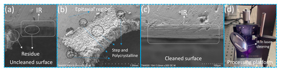
Figure 9.
Residues on IR and special processing substrate: (a) Residues on IR. (b) Steps on epitaxial layer and polycrystalline. (c) IR after cleaning. (d) Special IR processing substrate.
As shown in Figure 9b, single-crystal diamonds grow along the IR on the molybdenum substrate, extending to the epitaxial layer surface and forming steps and polycrystalline structures. To prevent contamination that could affect subsequent diamond single-crystal growth, femtosecond laser cleaning is employed. The laser focus is directed at these polycrystalline areas, using the same laser parameters to clean multiple times until the surface is clean and undamaged. This method effectively removes the steps and polycrystalline structures on the epitaxial layer, ensuring the quality of continuous single-crystal diamond growth. By carefully focusing the laser on the polycrystalline regions and utilizing optimal cleaning parameters, it is possible to eliminate unwanted growths without harming the underlying substrate. This ensures that the epitaxial layer remains smooth and free from contaminants, which is crucial for high-quality single-crystal diamond growth. The effectiveness of this approach demonstrates the precision and efficiency of femtosecond laser cleaning technology in maintaining the integrity of the substrate and facilitating superior diamond growth.
3.4. Laser Cleaning of Mo Substrate Cracks
Under the same experimental conditions, using parameter II, we performed femtosecond laser cleaning on both the FTR and IR surfaces, with a laser power of 2.38 W and a scanning speed of 1800 mm/s. After cleaning, we further studied the crack morphology on the molybdenum (Mo) substrate. As shown in Figure 10, the cleaned Mo substrate cracks are clear and smooth, with a width of 3 μm. This indicates that during the cleaning process, the femtosecond laser ablates the strip-shaped cracks on the Mo substrate, achieving thorough cleaning and surface smoothing. The EDS analysis results are shown in Table 3 (d), indicating that the Mo content after cleaning reached 86.24 wt%. This further confirms that femtosecond laser not only allows for cleaning minor damage on the molybdenum growth substrate but also significantly improves the cleaning effectiveness on the substrate cracks. By promptly repairing and cleaning the strip-shaped cracks in the Mo substrate, the quality and growth rate of single-crystal diamonds are enhanced, improving crystal quality and reducing energy consumption during growth. Therefore, femtosecond laser cleaning technology provides favorable conditions and environments for the regrowth of single-crystal diamonds while also laying the foundation for subsequent cleaning processes, further improving surface roughness and quality of the substrate. This advancement promotes development and applications in related technical fields.
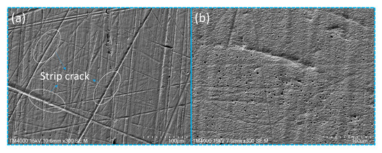
Figure 10.
Strip crack cleaning results: (a) Mo substrate strip crack. (b) Strip crack cleaning results.
4. Conclusions
This study investigated the multiple-scanning cleaning of non-uniform single and polycrystalline residues during single-crystal diamond growth on molybdenum growth substrates. At a laser power of 2.38 W, a repetition rate of 800 kHz, a scanning speed of 1800 mm/s, and a scanning interval of 10 μm, the MPCVD residues deposited on the FTR were found to aggregate into composite particles, removed through spalling caused by thermal expansion effects. In this situation, a complex tilted cleaning mechanism was employed to clear thick layered residues on the IR, where single-crystal diamonds on the FTR were reduced in thickness through gasification or elastic forces generated by reflected waves, followed by the removal of the remaining single-crystal diamonds via thermal expansion. Simultaneously, a positive defocusing laser with the same parameters effectively cleaned both the FTR and IR without damaging the substrate grooves of the growth base while also clearing clean cracks on the molybdenum substrate. By comparing the morphology and EDS characteristics of the substrate before and after cleaning, it can be seen that the femtosecond laser is accompanied by an instantaneous high temperature when removing polycrystalline diamonds. This indicates that the interaction of polycrystalline diamonds with femtosecond lasers is accompanied by the removal process of diamond graphitization and the mechanical exfoliation of the graphite layer substrate. This study not only provides a minor damage cleaning method for cleaning groove–inner wall structured growth bases but also has broad applicability for planar structure growth bases and even products like automobiles with decorative coatings. Therefore, replacing traditional chemical cleaning techniques with laser processes is beneficial, as it enhances mold lifespans and is environmentally friendly owing to eliminating chemical waste.
Author Contributions
Conceptualization, X.W.; methodology, X.C.; investigation, X.W.; writing—original draft preparation, X.W.; writing—review and editing, X.W.; supervision, X.W.; project administration, X.W.; funding acquisition, X.W. All authors have read and agreed to the published version of the manuscript.
Funding
This research was funded by the National Key Research and Development Program of China, No. 2021YFB3701800.
Data Availability Statement
The data are contained within the article.
Conflicts of Interest
Authors Xiwang Wu and Xin Chen were employed by the company Henan Huanghe Whirlwind Co., Ltd. The authors declare that the research was conducted in the absence of any commercial or financial relationships that could be construed as a potential conflict of interest.
References
- Sang, L. Diamond as the heat spreader for the thermal dissipation of GaN-based electronic devices. Funct. Diamond. 2021, 1, 174–188. [Google Scholar] [CrossRef]
- Wort, C.; Balmer, R. Diamond as an electronic material. Mater. Today 2008, 11, 22–28. [Google Scholar] [CrossRef]
- Yang, Z.; Liu, Y.; Guo, Z.; Wei, J.; Liu, J.; Chen, L.; Li, C. Deposition of uniform diamond films on three dimensional Si spheres by using faraday cage in MPCVD reactor. Diam. Relat. Mater. 2024, 142, 110767. [Google Scholar] [CrossRef]
- Wang, J.; Wang, X.; Li, X.; Wang, L.; Xu, F.; Zhang, B. Blue-white electroluminescence of diamond/WS2 quantum dot composite films. Diam. Relat. Mater. 2024, 143, 110941. [Google Scholar] [CrossRef]
- Bolshakov, A.; Ralchenko, V.; Shu, G.; Dai, B.; Yurov, V.; Bushuev, E.; Khomich, A.; Altakhov, A.; Ashkinazi, E.; Antonova, I.; et al. Single crystal diamond growth by MPCVD at subatmospheric pressures. Mater. Today Commun. 2020, 25, 101635. [Google Scholar] [CrossRef]
- Silva, F.; Achard, J.; Brinza, O.; Bonnin, X.; Hassouni, K.; Anthonis, A.; De Corte, K.; Barjon, J. High quality, large surface area, homoepitaxial MPACVD diamond growth. Diam. Relat. Mater. 2009, 18, 683–697. [Google Scholar] [CrossRef]
- Mokuno, Y.; Chayahara, A.; Soda, Y.; Yamada, H.; Horino, Y.; Fujimori, N. High rate homoepitaxial growth of diamond by microwave plasma CVD with nitrogen addition. Diam. Relat. Mater. 2006, 15, 455–459. [Google Scholar] [CrossRef]
- Liang, Q.; Yan, C.; Meng, Y.; Lai, J.; Krasnicki, S.; Mao, H.; Hemley, R. Recent advances in high-growth rate single-crystal CVD diamond. Diam. Relat. Mater. 2009, 18, 698–703. [Google Scholar] [CrossRef]
- Jia, X.; Dong, J.; Chen, Y.; Wang, H.; Zhu, G.; Kozlov, A.; Zhu, X. Nanosecond-millisecond combined pulse laser drilling of alumina ceramic. Opt. Lett. 2020, 45, 1691–1694. [Google Scholar] [CrossRef]
- Jia, X.; Chen, Y.; Wang, H.; Zhu, G.; Zhu, X. Experimental study on nanosecond-millisecond combined pulse laser drilling of alumina ceramic with different spot sizes. Opt. Laser Technol. 2020, 130, 160351. [Google Scholar] [CrossRef]
- Jia, X.; Zhang, Y.; Chen, Y.; Wang, H.; Zhu, G.; Zhu, X. Laser cleaning of slots of chrome-plated die. Opt. Laser Technol. 2019, 119, 105659. [Google Scholar] [CrossRef]
- Wang, Z.; Zeng, X.; Huang, W. Mechanism research of laser cleaning rubber layer on tire mold. In Proceedings of the International Conference on Industrial Lasers, Wuhan, China, 8 September 1999. [Google Scholar]
- Song, Y.; Wang, C.; Dong, X.; Yin, K.; Zhang, F.; Xie, Z.; Chu, D. Controllable superhydrophobic aluminum surfaces with tunable adhesion fabricated by femtosecond laser. Opt. Laser Technol. 2018, 102, 25–31. [Google Scholar] [CrossRef]
- Brand, J.; Maximova, K.; Madden, S.; Wain, A.; Rode, A.; Rapp, L. Femtosecond pulse laser cleaning of Makrana marble. Appl. Surf. Sci. 2023, 641, 158484. [Google Scholar] [CrossRef]
- Rivas, T.; Lopez, A.; Ramil, A.; Pozo, S.; Fiorucci, M.; de Silanes, M.; García, A.; de Aldana, J.; Romero, C.; Moreno, P. Comparative study of ornamental granite cleaning using femtosecond and nanosecond pulsed lasers. Appl. Surf. Sci. 2013, 278, 226–233. [Google Scholar] [CrossRef]
- Ersoy, T.; Tunay, T.; Uğuryol, M.; Mavili, G.; Akturk, S. Femtosecond laser cleaning of historical paper with sizing. J. Cult. Herit. 2014, 15, 258–265. [Google Scholar] [CrossRef]
- Maharjan, N.; Zhou, W.; Zheng, H.; Zhou, Y.; Wu, N. Surface Cleaning of a Titanium Alloy Using Femtosecond Laser Pulses. Laser Eng. 2019, 43, 223–235. [Google Scholar]
- Jia, X.; Chen, Y.; Liu, L.; Wang, C. Combined pulse laser: Reliable tool for high-quality, high-efficiency material processing. Opt. Laser Technol. 2022, 153, 108209. [Google Scholar] [CrossRef]
- Shin, S.; Hur, J.; Park, J.; Kim, D. Thermal damage free material processing using femtosecond laser pulses for fabricating fine metal masks: Influences of laser fluence and pulse repetition rate on processing quality. Opt. Laser Technol. 2021, 134, 106618. [Google Scholar] [CrossRef]
- Kononenko, T.; Meier, M.; Komlenok, M.; Pimenov, S.; Romano, V.; Pashinin, V.; Konov, V. Microstructuring of diamond bulk by IR femtosecond laser pulses. Appl. Phys. A 2008, 90, 645–651. [Google Scholar] [CrossRef]
- Chen, G.; Zhu, Z.; Yin, J.; Xiong, B.; Jin, M. Experiment on Ablation Threshold of Single Crystal Diamond Produced by Femtosecond Laser Processing. Chin. J. Lasers 2019, 46, 0402001. [Google Scholar]
- Yan, Y.; Zhang, S.; Zhao, X.; Han, Y.; Hou, L. Raman spectral research on MPCVD diamond film. Chin. Sci. Bull. 2003, 48, 2029–2030. [Google Scholar] [CrossRef]
- Zhang, X.; Chen, X.; Chen, T.; Ma, G.; Zhang, W.; Huang, L. Influence of Pulse Energy and Defocus Amount on the Mechanism and Surface Characteristics of Femtosecond Laser Polishing of SiC Ceramics. Micromachines 2022, 13, 1118. [Google Scholar] [CrossRef]
Disclaimer/Publisher’s Note: The statements, opinions and data contained in all publications are solely those of the individual author(s) and contributor(s) and not of MDPI and/or the editor(s). MDPI and/or the editor(s) disclaim responsibility for any injury to people or property resulting from any ideas, methods, instructions or products referred to in the content. |
© 2025 by the authors. Licensee MDPI, Basel, Switzerland. This article is an open access article distributed under the terms and conditions of the Creative Commons Attribution (CC BY) license (https://creativecommons.org/licenses/by/4.0/).