Article

Bismuth(III) Sulfide Films by Chemical Bath Deposition Method Using L-Cysteine as a Novel Sulfur Source

by
Aistis Melnikas
1,
Remigijus Ivanauskas
1,*,
Skirma Zalenkiene
1 and
Marius Mikolajūnas
2
1
Department of Physical and Inorganic Chemistry, Kaunas University of Technology, Radvilenu Str. 19, LT-50254 Kaunas, Lithuania
2
Faculty of Technology, State Higher Education Institution, Laisves Sq. 23, LT-35200 Panevezys, Lithuania
*
Author to whom correspondence should be addressed.
Crystals 2025, 15(6), 515; https://doi.org/10.3390/cryst15060515
Submission received: 12 March 2025 / Revised: 13 May 2025 / Accepted: 26 May 2025 / Published: 28 May 2025
(This article belongs to the Section Inorganic Crystalline Materials)

Abstract

Thin films of bismuth(III) sulfide (Bi2S3) on fluorine doped tin oxide (FTO) coated glass slides were successfully formed by the chemical bath deposition (CBD) method. In this work, a new sulfur precursor L-cysteine was used instead of the typical sulfur precursors, such as urea, thiosulfate, or thioacetamide, used for the formation of the Bi2S3 films by the CBD method. The synthesized Bi2S3 thin film on the FTO substrate was subjected to characterization techniques, including X-ray diffraction (XRD), scanning electron microscopy (SEM), energy dispersive X-ray spectroscopy (EDS), and UV–Visible spectroscopy analysis. An X-ray diffraction analysis showed that, initially, Bi2S3 films of an amorphous structure with elemental sulfur impurities were formed on the FTO surface. During the annealing of the samples, amorphous Bi2S3 was transformed into its crystalline phase with an average crystallite size of about 22.06 nm. The EDS studies confirmed that some of the sulfur that was not part of the Bi2S3 was removed from the films during annealing. The influence of the morphology of Bi2S3 films on their optical properties was confirmed by studies in the UV-visible range.

1. Introduction

Accelerating climate change, rapidly growing populations, and the resulting pollution are forcing a shift away from fossil fuels to clean and sustainable energy sources. Solar energy is one of these sources. It is imperative to develop innovative, efficient, and resource-saving solar energy technologies that have a lower impact on the environment. Non-toxic, earth abundant, and stable, bismuth is an ideal alternative to poisonous lead, cadmium, or mercury in environmentally friendly solar panels. Furthermore, non-toxic bismuth(III) sulfide (Bi2S3) thin films are of great interest as a component of solar cells due to their high efficiency for converting incoming photons into electrons. Bi2S3 is classified as an n-type semiconductor with a direct optical band gap between 1.3 and 2.2 eV, and with a high absorption coefficient of 105 cm–1 [1]. According to the Beer–Lambert law, a 200 nm thick Bi2S3 film can absorb 95% of the incident radiation [2]. Due to the optical and electro-optical properties of the Bi2S3 films, they are widely used in optoelectronic and thermoelectric devices, such as photo-catalysts [3], hydrogen storage [4], and the optical-detection for infrared [5] and UV light [6], among other uses. Furthermore, the Bi2S3 thin films can be used as efficient anode materials for lithium–ion batteries [7], as thermoelectric hydrogen [8] gas sensors [9], or memristors [10], and even for cancer diagnostics [11,12]. Bi2S3 thin films can be grown using physical processes, including spray pyrolysis [13], pulsed laser deposition [14], chemical vapor deposition [15], and thermal evaporation [16], among other processes. However, the above methods for forming Bi2S3 thin films have various disadvantages, such as requiring complex equipment, high temperature, ultrahigh vacuum environment, and high costs. While wet methods, such as chemical bath deposition (CBD) and successive ion layer adsorption and reaction (SILAR) of chalcogenide films, are very promising due to their low deposition costs, ease of equipment use, and large surface area deposition capability. The use of flow reactors in the process of film formation eliminates the influence of local fluctuations in the concentration or temperature gradient on the deposited film [17]. However, the most important advantage of this method is the ability to control the formation rate and the film thickness. During the formation of films by the CBD method, the substrate, and all cationic and anionic precursors are present in the same reaction bath. Thus, the reaction rate is controlled by the gradual release of metal ions from their chelate complexes, which then react with the sulfur ions to form a thin metal sulfide film. The film thickness can be controlled by varying the duration of the reaction. This allows for the production of films in one step, as well as the simultaneous control of film deposition. Therefore, in this work, the CBD method was used to form thin films of Bi2S3. The optoelectronic properties of films depend on their morphology, crystallinity, and the shape and size of the nanoparticles they contain. A wide range of the morphologies of Bi2S3 nanostructures is also known, such as stars, balls, belts, ribbons, flowers, snowflakes, tubes, rods, and wires [18]. The microstructure of sulfide films is significantly affected by sulfur sources [19,20] and the metal-to-sulfur ratio [20]. For the deposition of Bi2S3 thin films by the CBD method, thioacetamide, thiourea, and thiosulfate [21] are usually used as sulfur-releasing precursors.
A new precursor of sulfur for the formation of metal sulfide films may be L-cysteine, which has been studied much less than the precursors listed above. In its molecular structure, sulfur is present as a thiol group [–SH]. In addition, L-cysteine contains carboxyl [–COOH] and amino [–NH2] groups, which can bind protein biomolecules to metal electrodes, and gives it a unique metal-binding ability [22]. This makes L-cysteine one of the most versatile biomolecules for forming thin-layer bifunctional films. Furthermore, when combined with graphene oxide, it can be used for multicomponent synthesis as a reducible catalyst [23], for detection of toxic metal ions [24], for sensing in nanoarchitectonics [25], or for improving the anticorrosive properties of coatings [26]. Bi2S3 nanoparticles of various shapes and sizes and their heterostructures were synthesized using L-cysteine as a sulfur precursor using two-step hydrothermal [26,27,28] or solvothermal [29] methods. Meanwhile, the Bi2S3 layers were formed using L-cysteine by the electrodeposition method [30].
L-cysteine is considerably underexplored compared to the precursors listed above. The main drawback of L-cysteine as a sulfur precursor is its cost and relatively low sulfur content. By contrast, the selection of L-cysteine in our work was based out of scientific interest, as we found no existing work exploring its role in forming such metal sulfide films using the CBD route. The literature presents us with conflicting data on the effect of annealing on the film structure. Karsandik et al. [31] and Hussain et al. [32] reported the presence of the effect of annealing on the crystallite size and morphology of Bi2S3 films. However, Ahire et al. [33] noted no significant annealing effect on the crystalline structure of the films. Given these clashing confirmations, the main objective of this study was first to form Bi2S3 thin films on FTO substrates using the CBD wet chemistry method, then to anneal them and evaluate how this operation affects the crystallinity, morphological, and optical properties of these films.

2. Materials and Methods

2.1. Materials

For the synthesis of the Bi2S3 thin films, bismuth nitrate pentahydrate Bi(NO3)3·5H2O (99.99% purity) and L-cysteine (98.0% purity) were purchased from Sigma–Aldrich (Burlington, Massachusetts, United States). They were used as the precursors, while ethylenediaminetetraacetic acid disodium salt (EDTA-Na2) was used as a chelating agent. The fixanals of 0.1 mol/L nitric acid (Fluka, Buchs, Switzerland) and 0.025 mol/L EDTA-Na2 disodium salt solution (Chem-Lab, Zedelgem, Belgium) were also used to prepare solutions. Fluorine doped tin oxide (FTO) coated glass slides (by Merck, Rahway, NJ, USA) were used as substrates for the deposition of the Bi2S3 films. All materials were used as received.

2.2. Formation of the Bi2S3 Films

Pre-structured FTO slides (300 mm × 300 mm × 2.2 mm, surface resistivity ~7 Ω/sq) were cleaned with soapy water, then with acetone and distilled water in an ultrasonic bath, each step for 10 min, and finally dried in a desiccator over silica gel granules. The 0.1 mol/L bismuth precursor solution was prepared by dissolving 48.5 g Bi(NO3)3·5H2O in a minimum volume of 1 M nitric acid with magnetic stirring at 300 rpm until dissolved, and then diluted with distilled water to 1 L. The solution for the formation of the Bi2S3 films was prepared by mixing 25 mL of 0.1 mol/L Bi(NO3)3 solutions and 30 mL of 0.025 mol/L EDTA-Na2 solutions, followed by raising the temperature of the resulting solution to 80 °C and adding 1.0, 1.5, and 2.0 g (samples S1, S2, and S3) of L-cysteine powder while stirring. The concentrations of L-cysteine in the solutions prepared in this manner were 0.15, 0.23, and 0.30 mol/L, respectively. After 5 min, the FTO was immersed in this solution and kept there for 8 h. Zhang et al. [34] reported the co-precipitation of heavy metals, such as Cu(II), Pb(II), and Cd(II), from aqueous solutions using L-cysteine at 80 °C for 12 h. Since we did not find any information on the formation of Bi2S3 films on FTO substrates using the CBD method, these films were deposited under conditions similar to those described in the above-mentioned reference. When L-cysteine powder is added to the clear, colorless bismuth nitrate solution prepared for the experiment, the solution turns light yellow. This solution remains clear and light yellow throughout the experiment. Meanwhile, a black thin film of Bi2S3 gradually forms on the surface of the FTO slide. At the end of the experiment, the FTO slide samples were removed from the vessel, washed with distilled water for 20 s, dried in a desiccator for 24 h, and then used in further studies. Recently, it has been reported [35] that Bi2S3 films are partially oxidized to bismuth oxysulfate (Bi6S2O15) when annealed in an ambient atmosphere at temperatures of 360 °C and above. Therefore, the FTO slides with the Bi2S3 films were annealed in ambient atmosphere with a heating rate of 10 °C/min up to 300 °C. The samples were held at this temperature for 20 min and then allowed to cool naturally. The preparation of Bi2S3 films on the FTO slides by the CBD method are shown in Figure 1.

2.3. Characterization Methods of the Bi2S3 Films

An X-ray structural analysis of the Bi2S3 films formed on the FTO plates was performed using a D8 Advance diffractometer (Bruker AXS, Karlsruhe, Germany) with a high-speed one-dimensional Bruker LYNXEYE detector for recording diffraction patterns. The sizes of the Bi2S3 crystallites were calculated using the Scherrer formula based on the X-ray diffraction data along a given crystallographic plane as follows:
D = k λ β c o s θ
where D is the average crystallite size, λ is the X-ray wavelength (1.54178 Å), k is the shape factor (k = 0.9), θ = Bragg’s angle, and β is full-width at half-maximum (FWHM) of the peak. The phase composition of the formed films was determined using the Crystallographica Search-Match v. 2.1 and ConvX v. 1.0 software. The surface structure and morphology of the Bi2S3 thin films formed on the FTO plates were studied by scanning electron microscopy (SEM) using a Hitachi S–3400N scanning electron microscope (Chiyoda, Tokyo, Japan, magnification 1000× and 10,000×, scale 50 µm and 5 µm). The elemental composition of these films was determined by energy-dispersive X-ray spectroscopy (EDS) using an analyzer (JEOL-JSM 6360 A). The UV–Vis spectra were recorded at room temperature on a PerkinElmer Lambda 35 UV/VIS Spectrometer (Waltham, MA, USA). To compensate for the absorption of the PP strip band in the range of 200–900 nm, the Diffuse Reflectance Sphere Labsphere RSA-PE-20 was used.
A MarSurf WS1 (Göttingen, Germany) white light interferometer was used to measure the thickness of the film. First, on the prepared sample, a line was scratched diagonally in order to obtain the FTO glass, and then a picture of the sample surface was recorded. A point-measurement system was used. The heights between the FTO glass and the deposited film were measured, and this process was repeated 15 times at different parts of the film in order to measure the thickness precisely. Then, the average thicknesses were calculated.

3. Results and Discussion

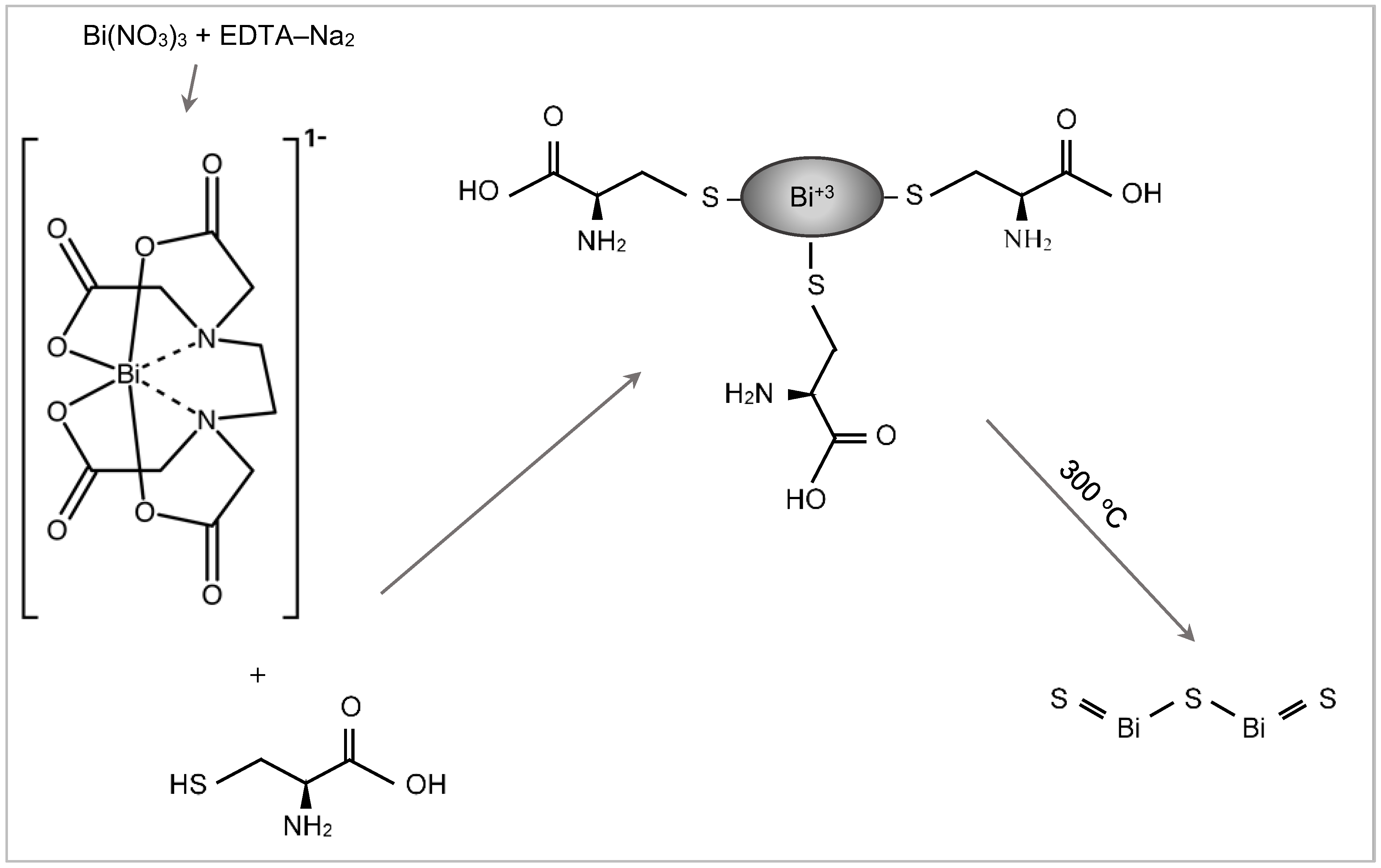
3.1. Bi2S3 Film Formation

A series of Bi2S3 films were formed on an FTO slide substrate using the CBD method, which maintains constant parameters under systematic variation of the sulfur precursor concentration. The probable process of formation of these films is shown schematically in Figure 2. Initially, Bi3+ forms ligand complexes with EDTA-Na2, which stabilize the Bi3+ ions and prevent their rapid hydrolysis in aqueous solution. El Adraa et al. recently reported [36] that L-cysteine formed a very stable chelate complex with heavy metal cations. Therefore, it is very likely that after L-cysteine dissolves in this solution, it reacts with Bi3+ ions, which are gradually released at higher temperatures due to hydrolysis of the chelate complex [37]. As a result of this reaction, complexes of bismuth with L-cysteine (Bi–LCy) are formed, which are deposited on the surface of the FTO plate. At the same time, hydrolysis of L-cysteine probably also occurs in the solution, leading to the formation of elemental sulfur. Salavati-Niasari et al. reported that a Bi complex containing L-cysteine decomposes at 180 °C for 5 h to form agglomerated Bi2S3 particles [38]. Finally, the FTO slides with the formed films were annealed at 300 °C for 20 min. At this temperature, the chelate complexes of bismuth with L-cysteine in the films was expected to decompose to form a crystalline Bi2S3 phase.

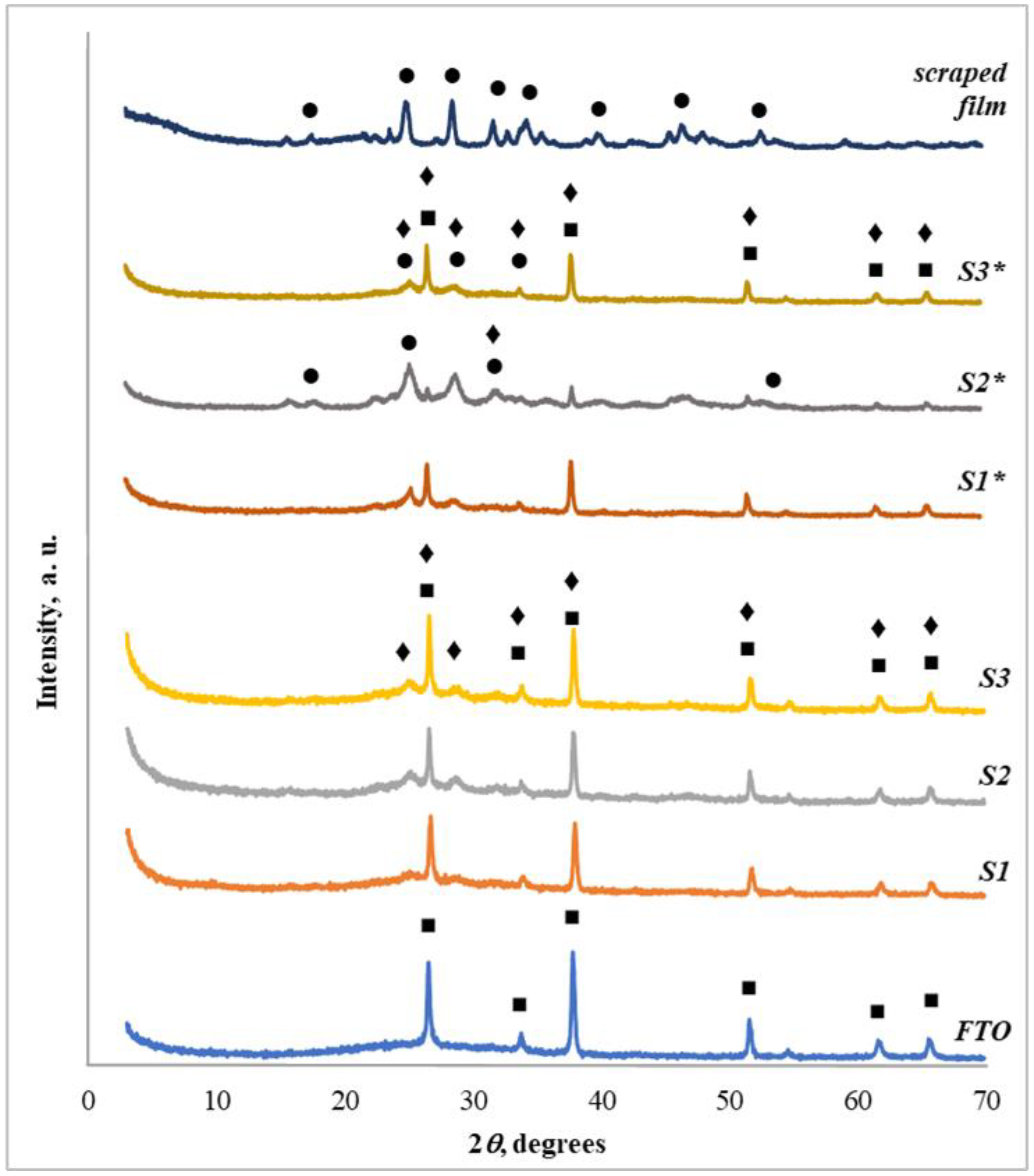
3.2. XRD Characterization

The structural characterization of the obtained Bi2S3 films on the FTO slides was carried out using X-ray diffraction. The XRD data of the Bi2S3 films were interpreted in detail using combinations of the data available in the literature [39,40,41] and the JCPDS reference templates. The results of the X-ray diffraction analysis are shown in Figure 3. Although the surface of samples 1–3 was obviously changed after the formation of the Bi2S3 films on them, the XRD patterns presented in Figure 3 do not show any peaks attributed to any bismuth(III) sulfide phase. Here, it can also be seen that the formed films contain a single-crystal phase of orthorhombic sulfur S8 (JCPDS: 83-2285). It is also important to note that six of the seven sulfur peaks, including the three most intense ones at 2θ = 26.66, 33.87 and 51.69°, overlap with the FTO peaks. Therefore, it is likely that the film formed on the FTO surface consists of the amorphous phase Bi2S3 or Bi–LCy and the crystalline phase of sulfur S8. The effect of annealing on the morphology, microstructure, crystallite size, phase composition, and optical properties of metal chalcogenide films on the surface of various carriers has been confirmed in our studies [42,43]. Therefore, in this work, we expected that the amorphous Bi2S3 would transform into a crystalline form during annealing. The X-ray diffraction patterns 1*–3* shown in Figure 3 confirmed that the films on the FTO slides formed a crystalline phase of orthorhombic bismuth(III) sulfide (JCPDS: 17-320) during the annealing process, with five peaks assigned to it at 2θ = 17.69, 25.20, 28.75, 31.89, and 52.56°. At the same time, from the peaks of the diffraction patterns shown in Figure 3, it can be said that the peaks of Bi2S3, elemental sulfur S8, and SnO2 are in very similar positions, and most of them overlap each other. Since the most intense peaks of the diffraction patterns of SnO2 and S8, such as 2θ = 26.66, 33.87, 37.91, 51.69, 61.74, and 65.72°, overlap, it is unclear whether sulfur remains in the film after annealing. To make sure that there was no sulfur left in the film after annealing, it was decided to remove the SnO2 peaks from its diffraction pattern. To accomplish this, part of the film formed after annealing was scraped off the FTO glass slide. If the scraped film contains sulfur, it will be visible in the diffraction pattern of this film. The most intense peaks of the crystalline phase of Bi2S3 are observed in the X-ray diffraction patterns of sample S2*, which indicates the formation of a film with the highest concentration of Bi2S3 on it. Therefore, the film was scraped off the surface of this sample and its diffraction pattern was recorded. This diffraction pattern is presented in Figure 3, which shows eight peaks of different intensities at 2θ = 17.43, 24.98, 28.67, 31.85, 35.51, 39.92, 46.42, and 52.52° attributed to the orthorhombic phase of Bi2S3 (JCPDS: 17-320). However, the diffraction pattern does not contain peaks that could be attributed to elemental sulfur. Therefore, the annealing of the deposited films is an important part of the formation of the crystalline Bi2S3 films on the FTO slide surface. Also, using the Scherrer formula, the crystallite size of the scraped film was estimated to be 22.0 ± 2 nm. Thus, the obtained X-ray diffraction data indicate that, after annealing, the orthorhombic phase Bi2S3 (JCPDS: 17-320) dominates in the film on the FTO slide of sample S2*. For example, the most intense peaks of the diffraction patterns, such as 2θ = 26.66, 33.87, 37.91, 51.69, 61.74, and 65.72°, can be attributed to SnO2 (JCPDS: 46-1088), which is located on the surface of the FTO glass slide.

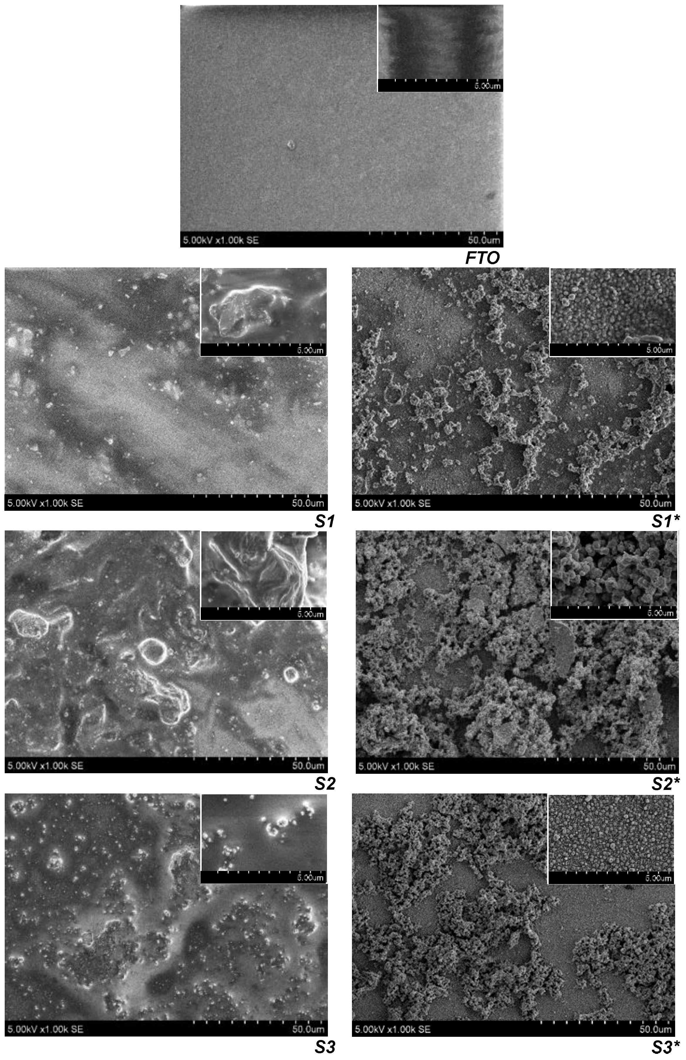
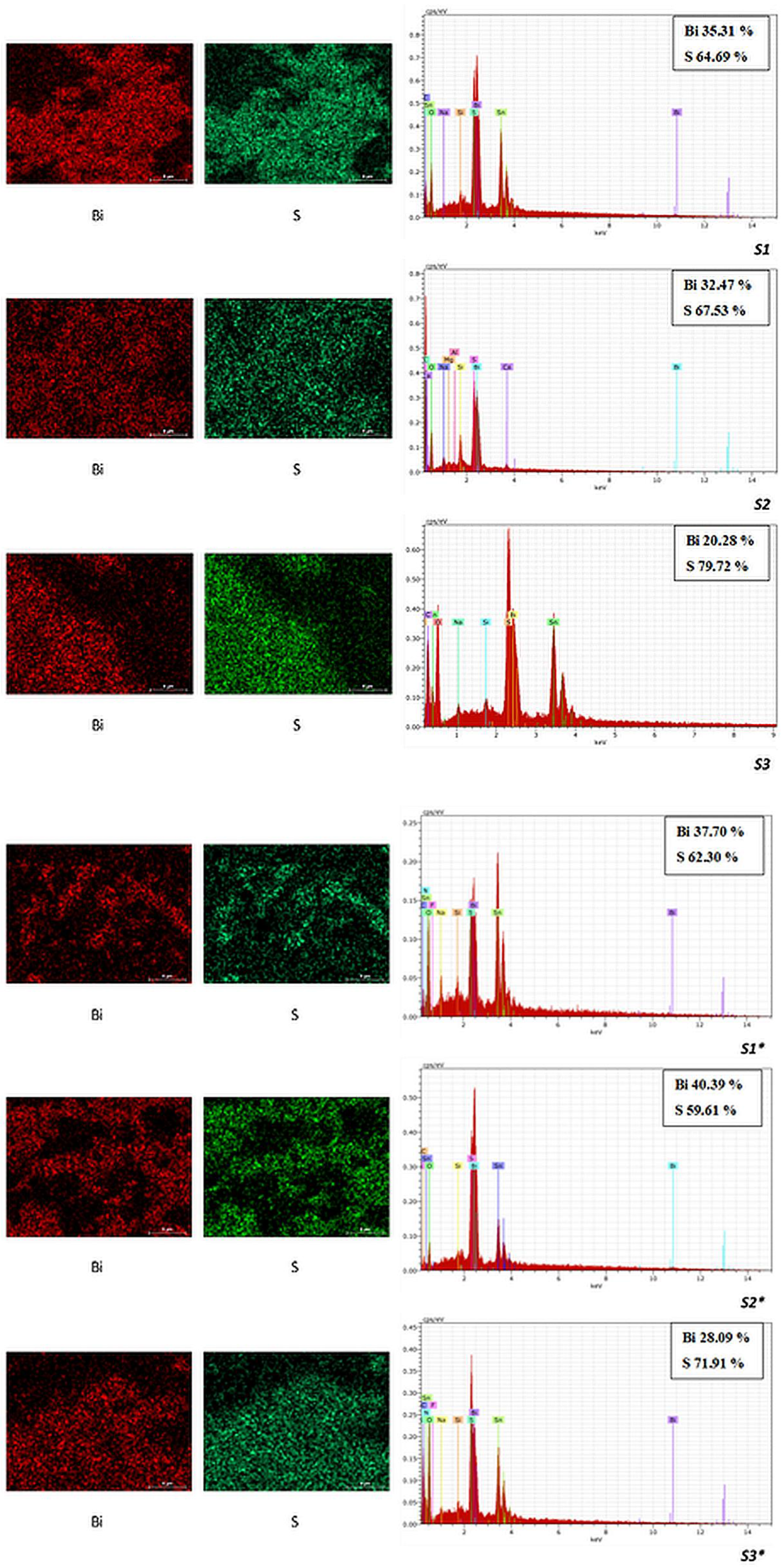
3.3. SEM/EDX Characterization

The surface morphology and elemental composition of the Bi2S3 thin films formed on the surface of the FTO slides were evaluated using scanning electron and energy dispersive X-ray spectroscopy. The SEM images of these films before and after annealing as well as the FTO slide without the film at different magnifications are shown in Figure 4. By comparing the SEM image of the FTO slide and samples S1–S3, it can be clearly stated that films were formed on the surface of the glass substrates. It is important to note that the SEM images of samples S1–S3 show typical amorphous layers with irregularly shaped particles and aggregates of different sizes, unevenly distributed over the entire surface area. The insets show that the particle and aggregate sizes vary widely from 10 nm to 5 µm. The surface morphology of the Bi2S3 films on the FTO slides changed dramatically after their annealing. As can be seen from the SEM images of samples S1*–S3* in Figure 4, the previously typical amorphous films were transformed into crystalline ones. The insets show that, after annealing, uniform, densely packed films containing nearly spherical particles or small grains of about 50 nm in size were formed on the surface of the FTO slides (Figure 4, sample S1* and S3*). In addition, part of the surface of these films is covered with clusters of agglomerates consisting of grains of irregular spherical shape. It is also clearly seen that the highest concentration of these clusters is on the surface of sample S2*.
The presence of stratified Bi2S3 films on the FTO slides was confirmed by elemental analysis using EDS. The analysis was conducted on the surface of the 50 × 45 µm FTO slides with the Bi2S3 film, as well as at a film depth of several micrometers. As can be seen from the results presented in Figure 5, in all the EDX spectra of the samples, the Bi and S peaks are clearly visible next to the extra ones, such as Na, Si, Sn, O, and F, which is due to the glass substrate or substrate holder used in the EDX instrument. There were no sources of these elements in the chemicals used to form the Bi2S3 film. In a number of studios, extra peaks of other elements were discarded and only the atomic percentages of Bi and S were considered [14,32,44]. Therefore, in this work, it was also decided to estimate only the atomic percentages of Bi and S. Based on these spectra and the elemental maps of Bi and S, the following observations can be made. First, the elemental mapping of Bi and S correlates, suggesting a uniform distribution of these elements on the surface of the FTO slides, confirming the formation of the stratified Bi2S3 films. Second, the intensity of the peaks in the EDX spectrum is directly proportional to the content of these elements. Thus, the predominance of the Bi and S peaks at 2.4 eV and 2.15 eV, respectively, over the peaks of other elements in samples S2, S2*, S3, and S3* directly indicates the highest concentration of bismuth(III) sulfide in the films formed on them. Finally, as can be seen from the inserts of the atomic percentages of bismuth and sulfur in the EDX spectra, in the unannealed Bi2S3 films, the atomic ratios of Bi and S vary in the ranges of 20.28–32.47% and 64.69–79.72%, respectively. This indicates an excess of sulfur in the films, and it is likely that the stoichiometric Bi2S3 was not formed. Riahi et al. [45] and Sonawane and Patil [44] reported that the atomic percentages of Bi of 40% and of S of 60% in the Bi2S3 films indicate the stoichiometric nature of these films. After annealing the films, the atomic percentage of Bi in all samples increased to 28.09–40.31%, while the atomic percentage of S decreased accordingly to 59.61–71.91%. Dachraoui et al. [46] formed stoichiometric orthorhombic phase Bi2S3 (JCPDS: 17-320) with Bi and S in a percentage ratio of 39.61:60.39% on glass microscopic specimens when thiourea was used as the sulfur precursor. The atomic percentages of Bi and S, 40.31 and 59.61%, respectively, are very similar to those in sample S2*, while the orthorhombic Bi2S3 (JCPDS: 17-320) phase in the film was confirmed by the X-ray diffraction analysis. Based on these data, it can be stated that a stoichiometric Bi2S3 film was formed on the surface of sample S2* after its annealing.

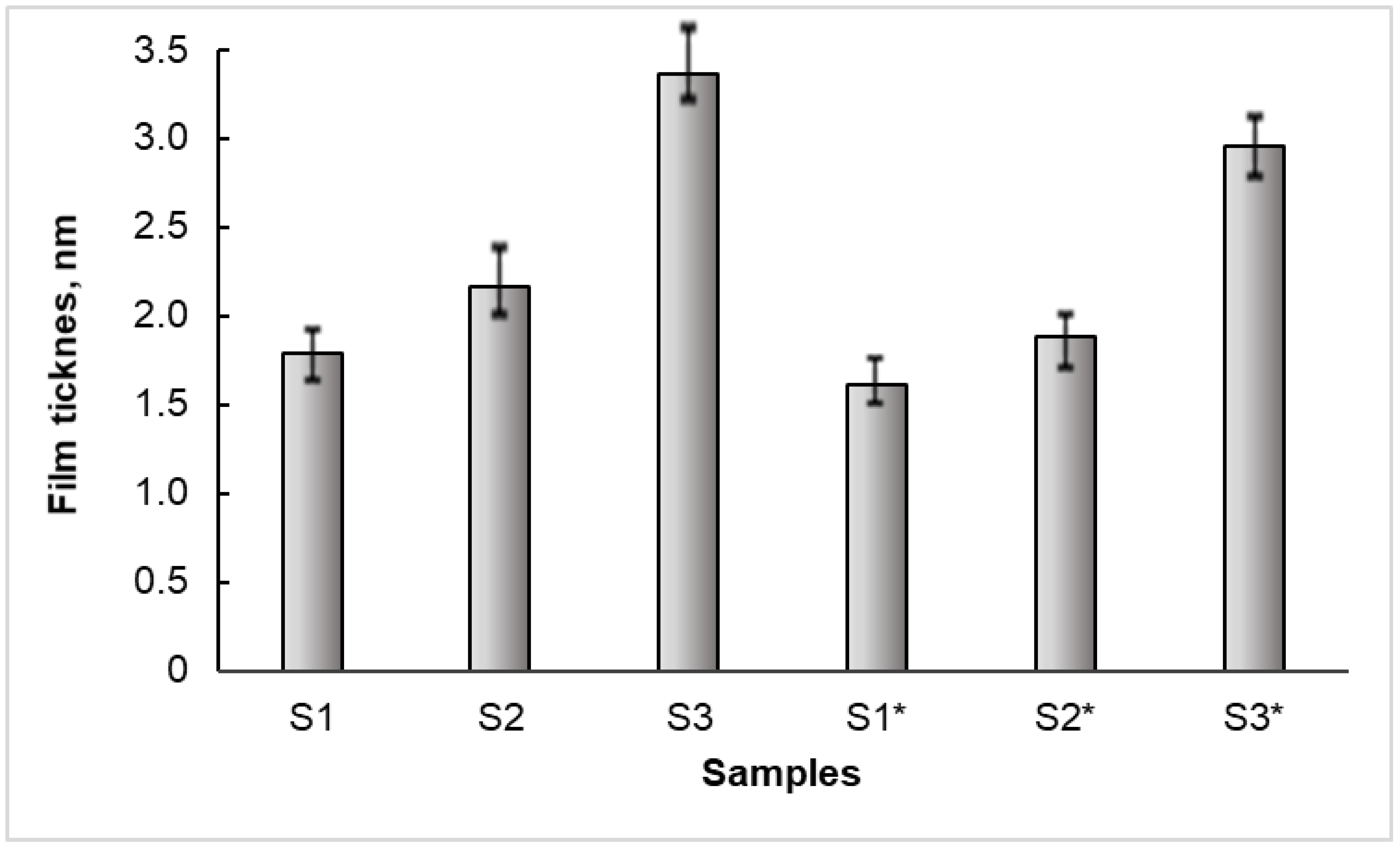
3.4. The Thickness of the Bi2S3 Films

It is well known that the film thickness applied to different materials can affect their thermal, mechanical, electrical, and optical properties [47]. To assess the dependence of the thickness of the films formed on the FTO slide substrate on the concentration of the sulfur precursor and the annealing process, a cross-sectional analysis was performed. The results of the analysis are presented in Figure 6, where it is evident that, with an increase in the concentration of the sulfur precursor, the film thickness increases from 1.79 to 3.37 µm. Meanwhile, after annealing, the thickness of all films decreased by ~10–12% from 1.62 to 2.96 µm. As already mentioned in reference [38], the Bi–L-cysteine complex decomposes at 180 °C and forms the agglomerated Bi2S3 particles. Therefore, it is most likely that, during annealing, the Bi–L-cysteine complexes in the film decompose under the influence of a temperature of 300 °C, forming a crystalline orthorhombic phase of Bi2S3. Along with this, oxidation of elemental sulfur in the film by atmospheric oxygen and its removal from the layer in the form of SO2 gas occurs. All this leads to a decrease in the volume of the film and, as a consequence, to a decrease in its thickness. Other researchers have also noted a decrease in the thickness of Bi2S3 films formed by the CBD method on a glass substrate using thioacetamide as a sulfur precursor after annealing them in air at 250 °C for 30 min or in an Ar plasma [21] or under a helium gas flow [48].

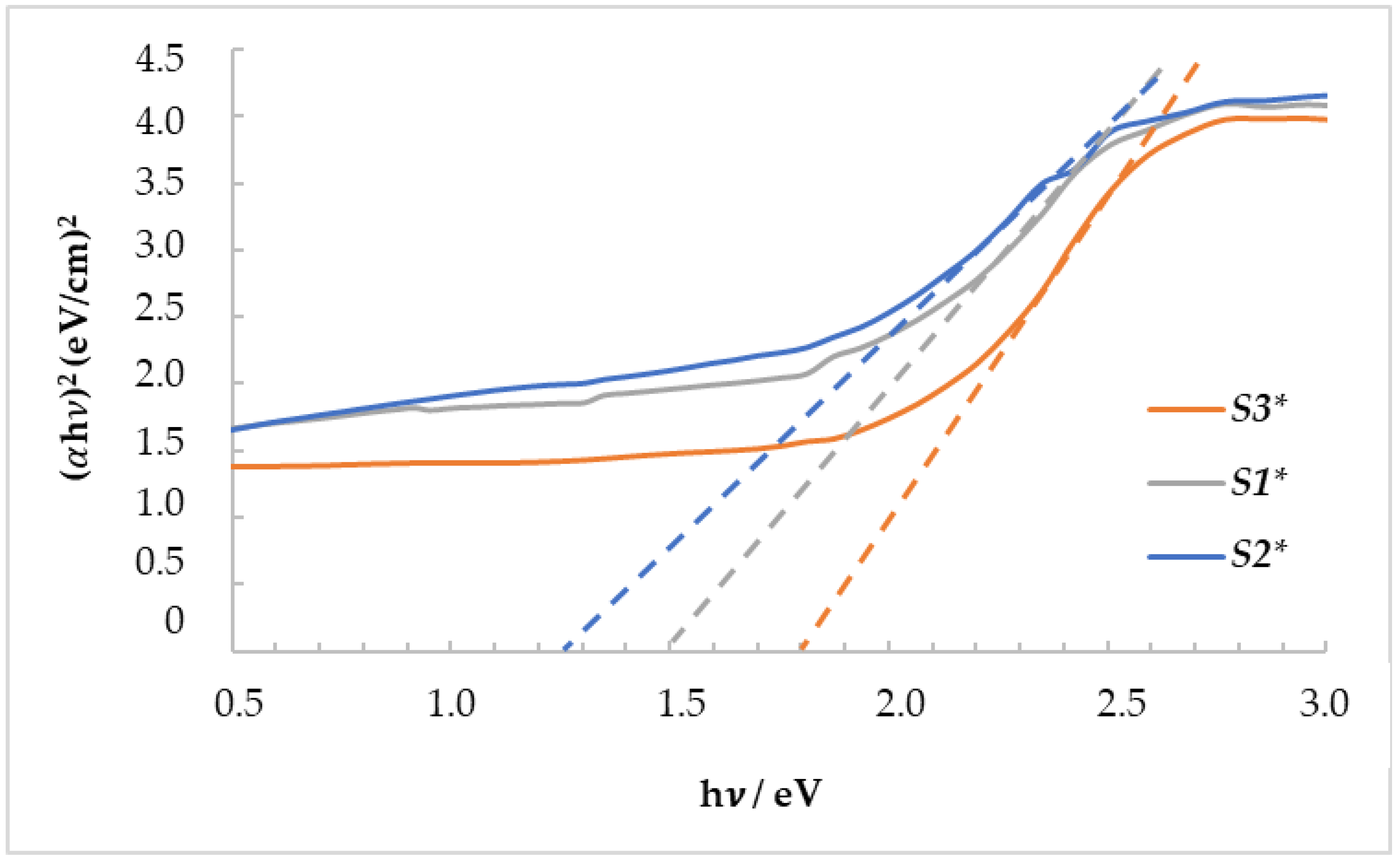
3.5. UV–Vis Spectroscopy Analysis

The optical transmittance of materials is their ability to transmit light through themselves. Optical transmittance plays a particularly important role in thin semiconductor films, since it directly affects the absorption coefficient and the band gap energy. The optical transparency of semiconductor films near the absorption edge drops sharply due to band-to-band transitions. The band gap (Eg) was calculated using Equation (2), which relates the photon energy in crystalline semiconductors to the following absorption coefficient [49]:
(αhν) = B(hν − Eg)n
where α is the absorption coefficient, B is a constant, coherent with absorption, is photon energy (eV), and n can have values of 1/2, 2, 3/2, and 3 for allowed direct, allowed indirect, forbidden direct, and forbidden indirect transitions, respectively.
Figure 7 and Figure 8 show the typical diagrams used to calculate the band gap values for samples S1–S3 and S1*–S3* before and after annealing, respectively. The band gap values for the unheated S1–S3 samples were found to be 3.35–3.95 eV. No evidence has been found in the literature that Bi2S3 thin films have such band values. As the XRD and SEM analyses of these samples show, this is most likely due to the amorphous structure of these films and their high crystalline sulfur content. However, after annealing the samples, it was found that the band gap of the films decreased up to 1.25–1.8 eV. This agrees well with the previously published values of the band gap for Bi2S3 films on glass substrate obtained by CBD followed by sulfurization in N2 atmosphere at 250–400 °C [50]. According to the XRD and SEM results, this sharp decrease in the band gap during annealing is attributed to improved film homogeneity and stoichiometry as well as sulfur removal from the films. According to Rincón et al. [51], the loss of sulfur during annealing favors the formation of crystalline Bi2S3 phases. Summarizing the UV studies, it should be emphasized that the S2* sample has a bandgap width of 1.25 eV at room temperature, the value of which provides the highest solar cell energy conversion efficiency according to the Shockley–Queisser limit for a single junction solar cell [52].

4. Conclusions

Bismuth(III) sulfide films on FTO glass slides were prepared by the CBD method using L-cysteine as the sulfur precursor. The influence of L-cysteine concentration and the annealing process of the Bi2S3 films on the FTO on the chemical, surface morphology, and phase composition of these films was studied. The XRD data showed that the as-formed films consisted of amorphous Bi2S3 and the crystalline phase of orthorhombic sulfur S8 (JCPDS: 83-2285). However, after annealing in these films, amorphous bismuth(III) sulfide or complexes of bismuth with L-cysteine were transformed into the crystalline form of Bi2S3. The EDX analysis showed that the atomic ratios of Bi and S on the surface of the S2* sample (40.31 and 59.61%) were in good agreement with the results of the studies [44,45,46], which confirmed the presence of the orthorhombic phase of Bi2S3 (JCPDS: 17-320) in this film. In addition, the EDX analysis showed that the Bi2S3 films on other samples contained excessive amounts of sulfur, which negatively affected the properties of these films. Therefore, it is necessary to conduct detailed studies of Bi2S3 films in order to determine the effect of annealing process conditions on the phase and elemental composition of these films. An SEM analysis confirmed the XRD results and showed that the typical amorphous Bi2S3 films were transformed into crystalline ones after annealing, and the surface of the FTO slides was partially covered by the formation of fine-grained agglomerates. The EDS results showed that some of the sulfur was removed from the films during the annealing process. The optical study of the Bi2S3 films revealed a huge influence of the annealing procedure on the bandgap width of these films. Before annealing the bandgap width of the samples was in the range of 3.35–3.95 eV, and after annealing it decreased more than twice to 1.25–1.8 eV. The studies carried out confirmed beyond a doubt that annealing of the samples is a prerequisite for the formation of crystalline Bi2S3 films on the surface of the FTO substrate. Therefore, this operation is one of the main strategies for further research in order to obtain films with a suitable band gap for use in the production of photovoltaic materials.

Author Contributions

Conceptualization, R.I.; Methodology, R.I. and M.M.; Software, A.M.; Formal analysis, A.M. and M.M.; Investigation, S.Z.; Data curation, S.Z.; Writing—original draft, R.I. All authors have read and agreed to the published version of the manuscript.

Funding

This research was funded by the Doctoral Fund of Kaunas University of Technology No. A-410, approved 26 June 2019.

Data Availability Statement

The original contributions presented in this study are included in the article. Further inquiries can be directed to the corresponding author(s).

Conflicts of Interest

The authors declare no conflict of interest.

References

  1. Supekar, A.T.; Bhujbal, P.K.; Salunke, S.A.; Rathod, S.M.; Patole, S.P.; Pathan, H.M. Bismuth Sulfide and Antimony Sulfide-Based Solar Cells: A Review. ES Energy Environ. 2023, 19, 848. [Google Scholar] [CrossRef]
  2. Fazal, T.; Ismail, B.; Shah, M.; Iqbal, S.; Elkaeed, E.B.; Awwad, N.S.; Ibrahium, H.A. Simplified Route for Deposition of Binary and Ternary Bismuth Sulphide Thin Films for Solar Cell Applications. Sustainability 2022, 14, 4603. [Google Scholar] [CrossRef]
  3. Renuka Devee, D.; Sivanesan, T.; Muthukrishnan, R.M.; Pourkodee, D.; Mohammed Yusuf Ansari, P.; Abdul Kader, S.M.; Ranjani, R. A novel photocatalytic activity of Bi2S3 nanoparticles for pharmaceutical and organic pollution removal in water remediation. Chem. Phys. Impact 2024, 8, 100605. [Google Scholar] [CrossRef]
  4. Razavi, F.S.; Mahdi, M.A.; Ghanbari, D.; Dawi, E.A.; Abed, M.J.; Ganduh, S.H.; Jasim, L.S.; Salavati-Niasari, M. Fabrication and design of four-component Bi2S3/CuFe2O4/CuO/Cu2O nanocomposite as new active materials for high performance electrochemical hydrogen storage application. J. Energy Storage 2024, 94, 112493. [Google Scholar] [CrossRef]
  5. Rong, P.; Gao, S.; Ren, S.; Lu, H.; Yan, J.; Li, L.; Zhang, M.; Han, Y.; Jiao, S.; Wang, J. Large-Area Freestanding Bi2S3 Nanofibrous Membranes for Fast Photoresponse Flexible IR Imaging Photodetector. Adv. Funct. Mater. 2023, 33, 2300159. [Google Scholar] [CrossRef]
  6. Singh, A.; Chauhan, P.; Verma, A.; Yadav, B.C. Interfacial engineering enables polyaniline-decorated bismuth sulfide nanorods towards ultrafast metal–semiconductor-metal UV-Vis broad spectra photodetector. Adv. Compos. Hybrid Mater. 2024, 7, 88. [Google Scholar] [CrossRef]
  7. Zhang, X.; Xie, J.; Tang, Y.; Lu, Z.; Hu, J.; Wang, Y.; Cao, Y. Oxygen Self-Doping Bi2S3@C Spheric Successfully Enhanced Long-Term Performance in Lithium-Ion Batteries. ACS Appl. Mater. Interfaces 2024, 16, 52423–52431. [Google Scholar] [CrossRef]
  8. Yu, Y.; Hu, Z.; Lien, S.-Y.; Yu, Y.; Gao, P. Self-Powered Thermoelectric Hydrogen Sensors Based on Low-Cost Bismuth Sulfide Thin Films: Quick Response at Room Temperature. ACS Appl. Mater. Interfaces 2022, 14, 47696–47705. [Google Scholar] [CrossRef]
  9. Kan, H.; Yang, W.; Guo, Z.; Li, M. Highly sensitive room-temperture NO2 gas sensor based on Bi2S3 nanorods. J. Mater. Sci. Mater. Electron. 2024, 35, 331. [Google Scholar] [CrossRef]
  10. Terdalkar, P.; Kumbhar, D.D.; Pawar, S.D.; Nirmal, K.A.; Kim, T.G.; Mukherjee, S.; Khot, K.V.; Dongale, T.D. Revealing switching statistics and artificial synaptic properties of Bi2S3 memristor. Solid State Electron. 2025, 225, 109076. [Google Scholar] [CrossRef]
  11. Zhao, Y.; Tao, Y.; Huang, Q.; Huang, J.; Kuang, J.; Gu, R.; Zeng, P.; Li, H.-Y.; Liang, H.; Liu, H. Electrochemical Biosensor Employing Bi2S3 Nanocrystals-Modified Electrode for Bladder Cancer Biomarker Detection. Chemosensors 2022, 10, 48. [Google Scholar] [CrossRef]
  12. Yang, Z.; Wang, L.; Zhang, J.; Liu, J.; Yu, X. Application of bismuth sulfide based nanomaterials in cancer diagnosis and treatment. Nano Today 2023, 49, 101799. [Google Scholar] [CrossRef]
  13. Bouachri, M.; Oubakalla, M.; El Farri, H.; Díaz-Guerra, C.; Mhalla, J.; Zimou, J.; El-Habib, A.; Beraich, M.; Nouneh, K.; Fahoume, M.; et al. Substrate temperature effects on the structural, morphological and optical properties of Bi2S3 thin films deposited by spray pyrolysis: An experimental and first-principles study. Opt. Mater. 2023, 135, 113215. [Google Scholar] [CrossRef]
  14. Rodríguez-Rosales, K.; Cruz-Gómez, J.; Cruz, J.S.; Guillén-Cervantes, A.; de Moure-Flores, F.; Villagrán-Muniz, M. Plasma emission spectroscopy for studying Bi2S3 produced by pulsed laser deposition and effects of substrate temperature on structural, morphological, and optical properties of thin films. Mater. Sci. Eng. B 2025, 312, 117867. [Google Scholar] [CrossRef]
  15. Atamtürk, U.; Jung, E.; Fischer, T.; Mathur, S. Tale of Two Bismuth Alkylthiolate Precursors’ Bifurcating Paths in Chemical Vapor Deposition. Chem. Mater. 2022, 34, 7344–7356. [Google Scholar] [CrossRef]
  16. Ran, Y.; Song, Y.; Jia, X.; Gu, P.; Cheng, Z.; Zhu, Y.; Wang, Q.; Pan, Y.; Li, Y.; Gao, Y.; et al. Large-Scale Vertically Interconnected Complementary Field-Effect Transistors Based on Thermal Evaporation. Small 2024, 20, 2309953. [Google Scholar] [CrossRef]
  17. Su, Y.-W.; Paul, B.K.; Chang, C.-H. Investigation of CdS nanoparticles formation and deposition by the continuous flow microreactor. Appl. Surf. Sci. 2019, 472, 158–164. [Google Scholar] [CrossRef]
  18. Ajiboye, T.O.; Onwudiwe, D.C. Bismuth sulfide based compounds: Properties, synthesis and applications. Results Chem. 2021, 3, 100151. [Google Scholar] [CrossRef]
  19. Mukurala, N.; Mishra, R.K.; Jin, S.H.; Kushwaha, A.K. Sulphur precursor dependent crystallinity and optical properties of solution grown Cu2FeSnS4 particles. Mater. Res. Express 2019, 6, 085099. [Google Scholar] [CrossRef]
  20. Behera, C.; Samal, R.; Panda, A.K.; Rout, C.S.; Samal, S.L. Synthesis of flower and biconcave shape CuS: Enhancement of super-capacitance properties via Ni–CuS nanocomposite formation. Solid. State Sci. 2021, 117, 106631. [Google Scholar] [CrossRef]
  21. Fazal, T.; Iqbal, S.; Shah, M.; Ismail, B.; Shaheen, N.; Alharthi, A.I.; Awwad, N.S.; Ibrahium, H.A. Correlation between structural, morphological and optical properties of Bi2S3 thin films deposited by various aqueous and non-aqueous chemical bath deposition methods. Results Phys. 2022, 40, 105817. [Google Scholar] [CrossRef]
  22. Koswattage, K.R.; Liyanage, C.J.; Maduwantha, G.D.K.V. Ultraviolet photoelectron spectroscopic study on the interface electronic structure of the L-cysteine on Pd surface. Surf. Interface Anal. 2022, 54, 561–566. [Google Scholar] [CrossRef]
  23. Toorbaf, M.; Moradi, L.; Dehghani, A. Preparation of GO/Cys-Cu(II) as a novel, effective and recoverable catalyst for the multi component synthesis of spirooxindoles under mild conditions. J. Mol. Struct. 2023, 1294, 136335. [Google Scholar] [CrossRef]
  24. Muralikrishna, S.; Sureshkumar, K.; Varley, T.S.; Nagaraju, D.H.; Ramakrishnappa, T. Ramakrishnappa, In situ reduction and functionalization of graphene oxide with L-cysteine for simultaneous electrochemical determination of cadmium(II), lead(II), copper(II), and mercury(II) ions. Anal. Methods 2014, 6, 8698–8705. [Google Scholar] [CrossRef]
  25. Melikyan, Y.; Gharagulyan, H.; Vasil’Ev, A.; Hayrapetyan, V.; Zhezhu, M.; Simonyan, A.; Ghazaryan, D.; Torosyan, M.; Kharatyan, A.; Michalicka, J.; et al. E-beam induced micropattern generation and amorphization of L-cysteine-functionalized graphene oxide nano-composites. Colloid Interface Sci. Commun. 2024, 58, 100766. [Google Scholar] [CrossRef]
  26. Javidparvar, A.A.; Naderi, R.; Ramezanzadeh, B. L-cysteine reduced/functionalized graphene oxide application as a smart/control release nanocarrier of sustainable cerium ions for epoxy coating anti-corrosion properties improvement. J. Hazard. Mater. 2020, 389, 122135. [Google Scholar] [CrossRef] [PubMed]
  27. Xiao, H.-J.; Liao, X.-J.; Wang, H.; Ren, S.-W.; Cao, J.-T.; Liu, Y.-M. In Situ Formation of Bi2MoO6-Bi2S3 Heterostructure: A Proof-Of-Concept Study for Photoelectrochemical Bioassay of l-Cysteine. Front. Chem. 2022, 10, 845617. [Google Scholar] [CrossRef]
  28. Yan, Y.; Chang, K.; Ni, T.; Li, K. l-cysteine assisted synthesis of Bi2S3 hollow sphere with enhanced near-infrared light harvesting for photothermal conversion and drug delivery. Mater. Lett. 2019, 245, 158–161. [Google Scholar] [CrossRef]
  29. Tao, X.; Hu, X.; Wen, Z.; Ming, Y.; Li, J.; Liu, Y.; Chen, R. Highly efficient Cr(VI) removal from industrial electroplating wastewater over Bi2S3 nanostructures prepared by dual sulfur-precursors: Insights on the promotion effect of sulfate ions. J. Hazard. Mater. 2022, 424, 127423. [Google Scholar] [CrossRef]
  30. Guo, R.; Zhu, G.; Gao, Y.; Li, B.; Gou, J.; Cheng, X. Synthesis of 3D Bi2S3/TiO2 NTAs photocatalytic system and its high visible light driven photocatalytic performance for organic compound degradation. Sep. Purif. Technol. 2019, 226, 315–322. [Google Scholar] [CrossRef]
  31. Karsandık, Ö.; Özdal, T.; Kavak, H. Influence of thickness and annealing temperature on properties of solution processed bismuth sulfide thin films. J. Mater. Sci. Mater. Electron. 2022, 33, 18014–18027. [Google Scholar] [CrossRef]
  32. Hussain, A.; Begum, A.; Rahman, A. Effects of annealing on nanocrystalline Bi2S3 thin films prepared by chemical bath deposition. Mater. Sci. Semicond. Process 2014, 21, 74–81. [Google Scholar] [CrossRef]
  33. Ahire, R.; Deshpande, N.; Gudage, Y.; Sagade, A.; Chavhan, S.; Phase, D.; Sharma, R. A comparative study of the physical properties of CdS, Bi2S3 and composite CdS–Bi2S3 thin films for photosensor application. Sens. Actuators A Phys. 2007, 140, 207–214. [Google Scholar] [CrossRef]
  34. Zhang, X.; Yan, L.; Li, J.; Yu, H. Adsorption of heavy metals by l-cysteine intercalated layered double hydroxide: Kinetic, isothermal and mechanistic studies. J. Colloid Interface Sci. 2020, 562, 149–158. [Google Scholar] [CrossRef]
  35. Khadka, D.B.; Kato, S.; Soga, T. Impact of annealing temperature on structural, optical and photovoltaic properties of bismuth oxysulfate thin films. Opt. Mater. 2024, 154, 115736. [Google Scholar] [CrossRef]
  36. El Adraa, K.; Georgelin, T.; Lambert, J.-F.; Jaber, F.; Tielens, F.; Jaber, M. Cysteine-montmorillonite composites for heavy metal cation complexation: A combined experimental and theoretical study. Chem. Eng. J. 2017, 314, 406–417. [Google Scholar] [CrossRef]
  37. Fazal, T.; Iqbal, S.; Shah, M.; Mahmood, Q.; Ismail, B.; Alzhrani, R.M.; Awwad, N.S.; Ibrahium, H.A.; Alam, S.; Yasir, M.; et al. Optoelectronic Analysis of Bismuth Sulfide and Copper-Doped Bismuth Sulfide Thin Films. JOM 2022, 74, 2809–2816. [Google Scholar] [CrossRef]
  38. Salavati-Niasari, M.; Behfard, Z.; Maddahfar, M. Controllable synthesis of Bi2S3 via a simple hydrothermal approach starting from an inorganic precursor. J. Ind. Eng. Chem. 2014, 20, 4066–4075. [Google Scholar] [CrossRef]
  39. Coppens, P.; Yang, Y.W.; Blessing, R.H.; Copper, W.F.; Larsen, F.K. The Experimental Charge Distribution in Sulfur Containing Molecules. Analysis of Cyclic Octasulfur at 300 and 100 K. J. Am. Chem. Soc. 1977, 99, 760–766. [Google Scholar] [CrossRef]
  40. Pekoite, CuPbBi 11 S 18, a New Member of the Bismuthinite-Aikinite Mineral Series; Its Crystal Structure and Relationship with Naturally- and Synthetically-Formed Members | The Canadian Mineralogist | GeoScienceWorld, (n.d.). Available online: https://pubs.geoscienceworld.org/mac/canmin/article-abstract/14/3/322/11114/Pekoite-CuPbBi-11-S-18-a-new-member-of-the (accessed on 11 March 2025).
  41. Vishwakarma, S.R.; Upadhyay, J.P.; Prasad, H.C. Physical properties of arsenic-doped tin oxide thin films. Thin Solid Film 1989, 176, 99–110. [Google Scholar] [CrossRef]
  42. Ivanauskas, R.; Samardokas, L.; Mikolajunas, M.; Virzonis, D.; Baltrusaitis, J. Polyamide–thallium selenide composite materials via temperature and pH controlled adsorption–diffusion method. Appl. Surf. Sci. 2014, 317, 818–827. [Google Scholar] [CrossRef]
  43. Ivanauskas, A.; Ivanauskas, R.; Ancutiene, I. Effect of In-Incorporation and Annealing on CuxSe Thin Films. Materials 2021, 14, 3810. [Google Scholar] [CrossRef] [PubMed]
  44. Sonawane, P.S.; Patil, L.A. Effect of nonstoichiometry on structural and optical properties of nanostructured Bi2S3 thin films prepared chemically at room temperature. Mater. Chem. Phys. 2007, 105, 157–161. [Google Scholar] [CrossRef]
  45. Riahi, M.; Martínez-Tomás, C.; Agouram, S.; Boukhachem, A.; Maghraoui-Meherzi, H. The effects of thermal treatment on structural, morphological and optical properties of electrochemically deposited Bi2S3 thin films. Thin Solid Film 2017, 626, 9–16. [Google Scholar] [CrossRef]
  46. Dachraoui, O.; Merino, J.M.; Mami, A.; León, M.; Caballero, R.; Maghraoui-Meherzi, H. Annealing study and thermal investigation on bismuth sulfide thin films prepared by chemical bath deposition in basic medium. Appl. Phys. A Mater. Sci. Process 2018, 124, 166. [Google Scholar] [CrossRef]
  47. Chanthong, T.; Intaratat, W.; Wichean, T.N. Effect of Thickness on Electrical and Optical Properties of ZnO:Al Films. Trends Sci. 2023, 20, 6372. [Google Scholar] [CrossRef]
  48. Moreno-García, H.; Messina, S.; Calixto-Rodriguez, M.; Martínez, H. Physical properties of chemically deposited Bi2S3 thin films using two post-deposition treatments. Appl. Surf. Sci. 2014, 311, 729–733. [Google Scholar] [CrossRef]
  49. Makuła, P.; Pacia, M.; Macyk, W. How To Correctly Determine the Band Gap Energy of Modified Semiconductor Photocatalysts Based on UV-Vis Spectra. J. Phys. Chem. Lett. 2018, 9, 6814–6817. [Google Scholar] [CrossRef]
  50. Krishna, V.G.; Reddy, G.P.; Revathi, N.; Reddy, K.T.R. Comprehensive physical and chemical properties of sulfurized Bi2S3 films prepared by CBD process. Next Mater. 2025, 8, 100566. [Google Scholar] [CrossRef]
  51. Rincón, M.E.; Campos, J.; Suárez, R. A comparison of the various thermal treatments of chemically deposited bismuth sulfide thin films and the effect on the structural and electrical properties. J. Phys. Chem. Solids 1999, 60, 385–392. [Google Scholar] [CrossRef]
  52. Linhart, W.M.; Zelewski, S.J.; Scharoch, P.; Dybała, F.; Kudrawiec, R. Nesting-like band gap in bismuth sulfide Bi2S3. J. Mater. Chem. C Mater. 2021, 9, 13733–13738. [Google Scholar] [CrossRef]
Figure 1. Scheme for obtaining Bi2S3 films on the FTO slides by the CBD method.
Crystals 15 00515 g001
Figure 2. Schematic illustration of the formation of Bi2S3 films using L-cysteine as a sulfur precursor.
Crystals 15 00515 g002
Figure 3. XRD patterns of the Bi2S3 films obtained on the FTO slides before (S1, S2, S3) and after (S1*, S2*, S3*) annealing, scraped film from sample S2* and the FTO glass slide. Peaks were identified and assigned as follows: (●)—Bi2S3 (JCPDS: 17-320) orthorhombic bismuth(III) sulfide; (◆)—S8 (JCPDS: 83-2285) orthorhombic sulfur; (■)—tetragonal SnO2 (JCPDS: 46-1088).
Crystals 15 00515 g003
Figure 4. Corresponding SEM surface images of the FTO slide and the Bi2S3 films on the FTO slides: samples S1, S2, S3 before annealing and samples S1*, S2*, S3* after annealing. High-resolution images of these films are shown in the corresponding insets.
Crystals 15 00515 g004
Figure 5. Chemical element maps and representative EDX spectra of the FTO slides with the Bi2S3 films. Samples S1, S2, S3 before annealing and samples S1*, S2*, S3* after annealing. The measured atomic percentages of Bi and S in the films are shown in the corresponding insets.
Crystals 15 00515 g005
Figure 6. Thicknesses of the Bi2S3 films on the FTO slides formed using different amounts of sulfur precursor before (S1, S2, S3) and after (S1*, S2*, S3*) annealing.
Crystals 15 00515 g006
Figure 7. Plot of (αhv)2 versus (hv) for determining the optical band gap of the FTO slides with the Bi2S3 film before annealing.
Crystals 15 00515 g007
Figure 8. Plot of (αhv)2 versus (hv) for determining the optical band gap of the FTO slides with the Bi2S3 film after annealing.
Crystals 15 00515 g008
Disclaimer/Publisher’s Note: The statements, opinions and data contained in all publications are solely those of the individual author(s) and contributor(s) and not of MDPI and/or the editor(s). MDPI and/or the editor(s) disclaim responsibility for any injury to people or property resulting from any ideas, methods, instructions or products referred to in the content.

