Article

Molecular Dynamics Study of Nanoscratching Behavior of Water-Film-Covered GaN (0001) Surface Using Spherical Diamond Abrasive

School of Mechanical Engineering, University of South China, Hengyang 421001, China
*
Author to whom correspondence should be addressed.
Crystals 2025, 15(5), 428; https://doi.org/10.3390/cryst15050428
Submission received: 31 March 2025 / Revised: 24 April 2025 / Accepted: 28 April 2025 / Published: 30 April 2025

Abstract

:
Molecular dynamics (MD) simulation of nanoscratching with a spherical diamond abrasive was performed to investigate the role of water molecular film on the surface nanotribological characteristics and subsurface lattice damage of GaN (0001) at the atomic level. The simulation results indicate that the tangential and normal forces exhibited no significant variation trend with the increase in water film thickness. Inducing a water film can alleviate the material pile-up during scratching, and the GaN surface obtained the lowest friction coefficient and wear volume when the water film thickness reached 3 nm, primarily due to the enhanced lubrication and the heat absorption by the water film in this case. Water-film-covered GaN exhibited a thinner subsurface damage layer than the bare GaN, and the damage layer thickness decreased with the increase in water film thickness for various scratching depths of 1 to 4 nm. For each scratching depth, there was an optimal water film thickness causing the minimum number of amorphization atoms. Nevertheless, the water film failed to inhibit the formation and propagation of dislocations in the scratching process, and water-film-covered GaN exhibited more dislocations than the bare one. This research has the potential to expand the comprehension of water-mediated nanotribology and the ultra-precision machining procedures of GaN.

1. Introduction

Gallium nitride (GaN), a representative of third-generation semiconductor materials, possesses remarkable properties including a wide bandgap, high thermal conductivity, and notable hardness. These features render it highly applicable in various fields like microelectronic devices, optoelectronics, and fifth-generation communications [1,2,3,4,5]. Ultra-precision machining techniques, mainly consisting of surface grinding and chemical-mechanical polishing (CMP), are the key technologies to realize the above applications of GaN materials. The material removal rate is low, and the processing-induced damage is prone to form during ultra-precision surface processing of GaN, primarily due to its hard-brittle properties [6,7,8]. These damages may reduce the reliability of the semiconductor devices and shorten their service life [9]. The mechanism of material removal in ultra-precision machining can be regarded as the degradation of materials from the nanoscale down to the atomic scale. It happens in either single or combined energy fields and under different environmental media [10]. Gaining insights into the nanotribological behavior of GaN can help develop high-efficiency, low-destructive ultra-precision surface machining technology.
The current ultra-precision surface processing of GaN single crystal mainly involves mechanical grinding, polishing, and CMP. Many scholars have studied the grinding and polishing processing of GaN and obtained many valuable results. Through the grinding experiment of GaN wafers with different slurries, Xu et al. [11] explored how the size of abrasives and the pressure applied on the wafer impacted the material’s grinding rate and surface quality. Weyher [12] et al. reported chemical polishing of GaN crystals using alkaline solutions at room temperature. They found that when a soft polishing pad was used and relatively high pressure was applied, a damage-free GaN surface could be obtained through CMP. Lee et al. [13] conducted an observation of the subsurface morphology of single-crystalline GaN after mechanical polishing and CMP through transmission electron microscopy, suggesting that the depth of the damage layer on the GaN substrate was related to the size of the diamond abrasive grains used. In the above ultra-precision surface processing, polishing fluids play an essential role in obtaining defect-free surfaces and improving machining efficiency [14,15,16]. Water, which serves as the primary ingredient in polishing fluids and functions as a lubricant, effectively contributes to the improvement of workpiece surface quality and the reduction of abrasive wear. The water-lubricated surface finishing process caused by abrasives occurs partly at the nanoscale level and can extend as far as the atomic scale. It is hard to elucidate experimentally the influence mechanism of water molecular films on the subsurface damage and surface material removal; the latter can be attributed to the nanoscale or atomic scale frication and wear problems.
Plenty of studies have proved that MD simulation can effectively reveal the surface nanotribological properties and structural transformation in the subsurface at atomic level [17,18,19,20,21]. For instance, Tian et al. [22] conducted a study using MD simulation to explore the impact of the water film on the sliding friction behavior of nanoparticles on Cu/Ag bilayers, and they found that selecting an appropriate water dosage can enhance the working performance of the bilayers. Zhou et al. [23] constructed an MD model for investigating the nano-cutting operation of 4H-SiC in an environment with water moisture. The simulation outcomes presented by them suggest that the water film is capable of decreasing the friction coefficient and improving the heat dissipation during the scratching process. Li et al. [24] used MD simulations to study the sapphire polishing process under water lubrication conditions, indicating that the water lubrication environment can alter the adhesion between the abrasive and the workpiece atoms and hence improve the wear resistance and surface quality. For instance, Wang et al. [25] investigated the influence of the sliding speed of the single abrasive grain on the material removal behavior during nanoscratching of Inva alloy through MD simulation, finding that choosing the right thickness of the water film along with an appropriate polishing velocity can substantially lower the workpiece’s surface roughness and get rid of subsurface defects. These scholars - obtained some similar conclusions that the water film can lower the friction coefficient and boost the heat dissipation performance of the scratching process, thus reducing the frictional wear for the hard-brittle materials [26,27,28,29]. Nevertheless, the roles of water molecular film with severe nanometer thickness on the nanotribological properties involving the nanoscale to atomic material removal behavior, as well as the subsurface lattice damage of monocrystalline GaN, remain unclear.
In this work, we investigated the influence of water molecular film on the surface nanotribological properties and subsurface lattice damage of GaN workpieces through MD simulation of nanoscratching under different water film thicknesses and scratching depths. Effects of water film on friction force, coefficient of friction, wear volume, structural transition, and stress and temperature distributions are clarified. The influence mechanism of the water molecule layer on the surface nanotribological properties and the scratching-induced lattice damage in the subsurface during the nanoscratching of GaN is discussed at the atomic scale. This study can enhance the understanding of water film effects on the water-mediated nanotribological and ultra-precision machining processes of GaN.

2. Materials and Methods

Figure 1 shows the molecular dynamics (MD) model of a nanoscratching consisting of a GaN (0001) workpiece covered with a water film and a spherical diamond abrasive. The size of the GaN workpiece was 30 nm (x-axis) × 20 nm (y-axis) × 15 nm (z-axis) along [1-210], [10-10], and [0001], respectively. The atomic number of GaN workpieces was 797, 525, and that of diamond abrasive particles was 47, 296. The spherical diamond abrasive with a radius of 4 nm was placed 1 nm above the GaN workpiece/water film before scratching. Five water films with thicknesses of 0.5, 1, 1.5, 2, and 3 nm were established in the MD model. During scratching, the diamond abrasive slid on the GaN (0001) surface along the [11-20] crystallographic direction at a sliding speed of 40 m/s; the utmost scratching extent (L) was 10 nm, and the scratching depths (d) were picked as 1, 2, 3, and 4 nm. The starting temperature of the water film was configured as 293 K, and a reflective wall was set up above the water film to stop the evaporation of water molecules. The elaborate simulation parameters are enumerated in Table 1, periodic boundary limitations were employed in the x and y directions to steer clear of boundary and size influences, and a fixed boundary was located in the z-direction. The GaN workpiece was partitioned into three sections from the bottom up, namely, the boundary layer, the thermostat layer, and the Newton layer. Thereinto, the dimensions of the Newtonian layer were 30 nm × 20 nm × 12 nm, and the boundary layer was fixed to maintain the position of the GaN workpiece and to perform the indentation and scratching simulation. The Langevin temperature control method was applied to the thermostatic layer in the indentation and scratching process. The movement of atoms within the Newtonian layer and the thermostat layer adhered to the classical Newtonian laws of motion. Their equations of motion were solved using the Velocity–Verlet numerical integration method.
In this study, the Stillinger–Weber (SW) potential function was used to describe the interactions within GaN, i.e., Ga-Ga, N-N, and Ga-N interactions; the 6-12 Lennard–Jones (L-J) potential function was used to describe the interactions between diamond abrasive grains (C) and GaN and H2O molecules; and the 12-12 L-J potential function was used to depict the interaction of O-O within the H2O molecule. For specific parameters, please refer to Table 2. Since the hardness of the diamond was much higher than that of GaN, the diamond abrasive was treated as a rigid body in our MD simulation.
The GaN\water film model was built by using a large-scale atomic/molecular massively parallel simulator (LAMMPS, Version 12 December 2018, Sandia National Laboratories) [32] and Materials Studio (MS 2020, Accelrys, San Diego, CA, USA) [33] software. The model was relaxed for 100 ps to reach a thermodynamic equilibrium state before the formal simulation that contained three stages of loading (indentation), scratching, and unloading stages. During the indentation procedure, the diamond abrasive advanced towards the GaN (0001) surface along the [000-1] crystal direction at a constant speed of 40 m/s until the predetermined indentation depth was reached. Then, the diamond abrasive scratched the GaN (0001) surface along the [10-12] crystal orientation with a velocity of 40 m/s. Finally, the diamond abrasive was retracted from the GaN workpiece to its original height, thereby concluding the unloading procedure. The simulation data were subsequently analyzed in depth using the visualization software Open Visualization Tool (OVTIO) 3.7.4 [29]. Many methods including identifying diamond structure (IDS) and the dislocation extraction algorithm (DXA) were comprehensively applied to meticulously analyze the structural characteristics of GaN crystals in the nanoscratching process.

3. Results and Discussion

3.1. Nanoindentation Properties

The influence of water molecule film with a thickness of several nanometers on the nanoindentation behavior of GaN workpieces was first investigated through MD simulation. Figure 2 illustrates the deformed morphology of GaN workpieces covered with different thicknesses of water films when the diamond indenter penetrated the GaN with 2 nm depth. Simulation results indicated that the presence of the water film can reduce the range of deformation and the material pile-up during nanoindentation due to the alleviation in the distribution of the stress fields. However, the alleviation of stress caused by the water film did not always work with the increasing thickness of the water film. There existed a thickness of the water film at which the indentation deformation was the slightest. The cross-sectional profiles of the various GaN workpieces when the indentation depth reached 2 nm are displayed in Figure 3. The top-row cloud maps depict the hydrostatic pressure distribution, whereas the bottom-row diagrams reveal the cross-sectional structural characteristics by shading atoms according to their IDS classifications. The water film led to a reduction in the contact area between the abrasive and workpiece and induced changes in stress distribution during their interaction, which ultimately mitigated the transformation of GaN from hexagonal diamond to cubic diamond structure and amorphous phase.

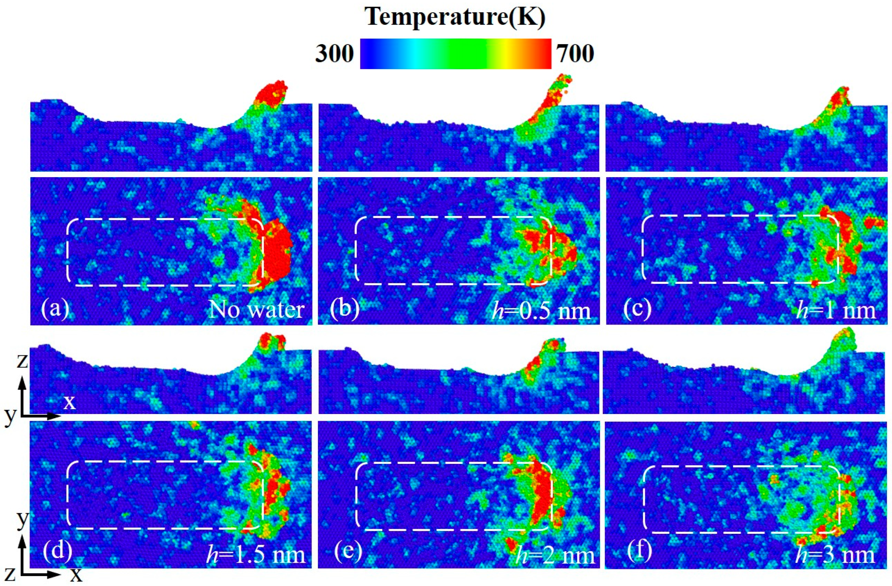
3.2. Nanotribological Performance

The evolution of the tangential force and normal force during nanoscratching of the above-mentioned workpieces at different scratching depths is given in Figure 4. At the initial scratching stage, the instantaneous acceleration induced an elastic shock due to the sudden change of the abrasive grains from loading along the [000-1] direction to scratching along [10-12], resulting in a rapid increase in friction force and the decrease in normal force. As the scratching proceeded and the stress reached the yield strength of GaN crystal, dislocation-dominated plastic removal occurred through activating a new slip regime. The friction force leveled off during the stable plastic removal stage when the scratching distance exceeded 2 nm [34]. In addition, both friction force and normal force increased with the increase in the scratching depth, as a greater scratching depth resulted in a larger contact abrasive–workpiece contact area.
The average tangential force, normal force, and friction coefficient for the steady-state scratching stage under different conditions are summarized in Figure 5. The simulation results reveal that the tangential and normal forces exhibited no significant variation trend with increasing water film thickness from 0 to 3 nm, attributed to the competing effects of lubrication and movement obstruction of the water molecules during scratching. During scratching, the diamond abrasive needed to push the surrounding water molecules to keep it moving and remove material, which brought greater friction and normal forces [29]. In addition, the water film did not exhibit an obvious lubrication effect, and the friction coefficient was similar under various water film thickness conditions. When the scratching depth was 1 nm, the friction coefficient fluctuated with the increase in the water film thickness. At this time, the deformation behavior of the GaN workpiece was in the elastic-plastic transformation zone, and only slight wear occurred. For other scratching depths, the friction coefficient for the GaN workpiece without water film was higher in most cases than that for the GaN workpiece covered with water film. When the thickness of the water film reached 3 nm, the friction coefficient for various scratching depth conditions exhibited the minimum value.
Moreover, the effect of water molecule film on the wear properties of GaN during nanoscratching was also investigated. Figure 6 shows the surface wear morphologies of GaN workpieces covered with different thicknesses of water film after scratching. The water film was hidden, and Ga and N atoms were colored according to their height in the Z direction in this figure to capture the surface wear and subsurface damage of the GaN workpiece. It was indicated that water film can alleviate the material pile-up of GaN, and hence the pile-up height decreased with the increase in the thickness of the water film. This is because the water molecules in the scratching process affected the plastic flow of the material and the formation of chips. The greater the water film thickness, the more pronounced the inhibition effect. In addition, compared with the bare GaN workpiece surface, the groove formed on the water-film-covered GaN workpiece surface was narrower. This is because the water film can disperse the stress in the GaN workpiece, resulting in a decrease in the effective range of stress. Figure 7 illustrates the von Mises stress distribution inside the workpiece after abrasive withdrawal. Following the withdrawal of the abrasive from the GaN workpiece, it can be observed that residual internal stresses existed in the workpiece for all water film thicknesses. Compared with the case without water film, the distribution of residual stresses in the GaN workpiece covered with water film was more dispersed, suggesting the internal stresses can be regulated by the water film.
Subsequently, the wear volume and wear rate of GaN workpieces covered by various films with different thicknesses were calculated, as shown in Figure 8. The water film exhibited an evident influence on the wear volume and wear rate of GaN workpieces. As the thickness of the water film increased from 0 to 3 nm, the wear volume decreased first, then increased, and decreased again when the water film thickness reached 3 nm, at which the wear volume obtained the lowest value. On the one hand, water film can first play a lubricating effect and weaken the direct contact of the diamond abrasive and the GaN workpiece, thus reducing the wear on the workpiece. On the other hand, the water film almost brought additional inhibition in the diamond abrasive scratching process. When the thickness of the water film reached a certain thickness, the resistance effect was higher than the lubrication one, and the wear of the GaN workpiece was promoted. Due to the different resistances at different scratching depths, the position of the “inflection point” corresponding to different scratching depths was not the same. For the scratching depths of 1, 2, 3, and 4 nm, the minimum wear volumes were 64.1, 82.9, 159.8, and 285.4 nm3, respectively, corresponding to water film thicknesses of 3, 1, 0.5, and 3 nm. When the water film thickness was 3 nm, the wear volume of the GaN workpiece demonstrated the lowest value due to the evident lubrication effect of the water film. To assess the rate of material removal, the wear rate is computed using the following formula:
δ = V ( n m 3 ) F n   ( n N ) × L ( n m )
where δ is the wear rate with a unit of nm3/nN·nm, V is the wear volume, Fn is the average normal force during scratching, and L is the scratching distance. Figure 8b shows the variation of wear rate with the water film thickness for different scratching depths. The findings indicate that the presence of a water film can, to a certain degree, diminish the wear rate of the GaN workpiece. Additionally, the lowest wear rate was achieved at the scratching depth of 2 nm. This is because there was not much difference in wear volume at lower scratch depths, but a scratching depth of 2 nm resulted in a greater normal force, which ultimately led to the lowest wear rate.

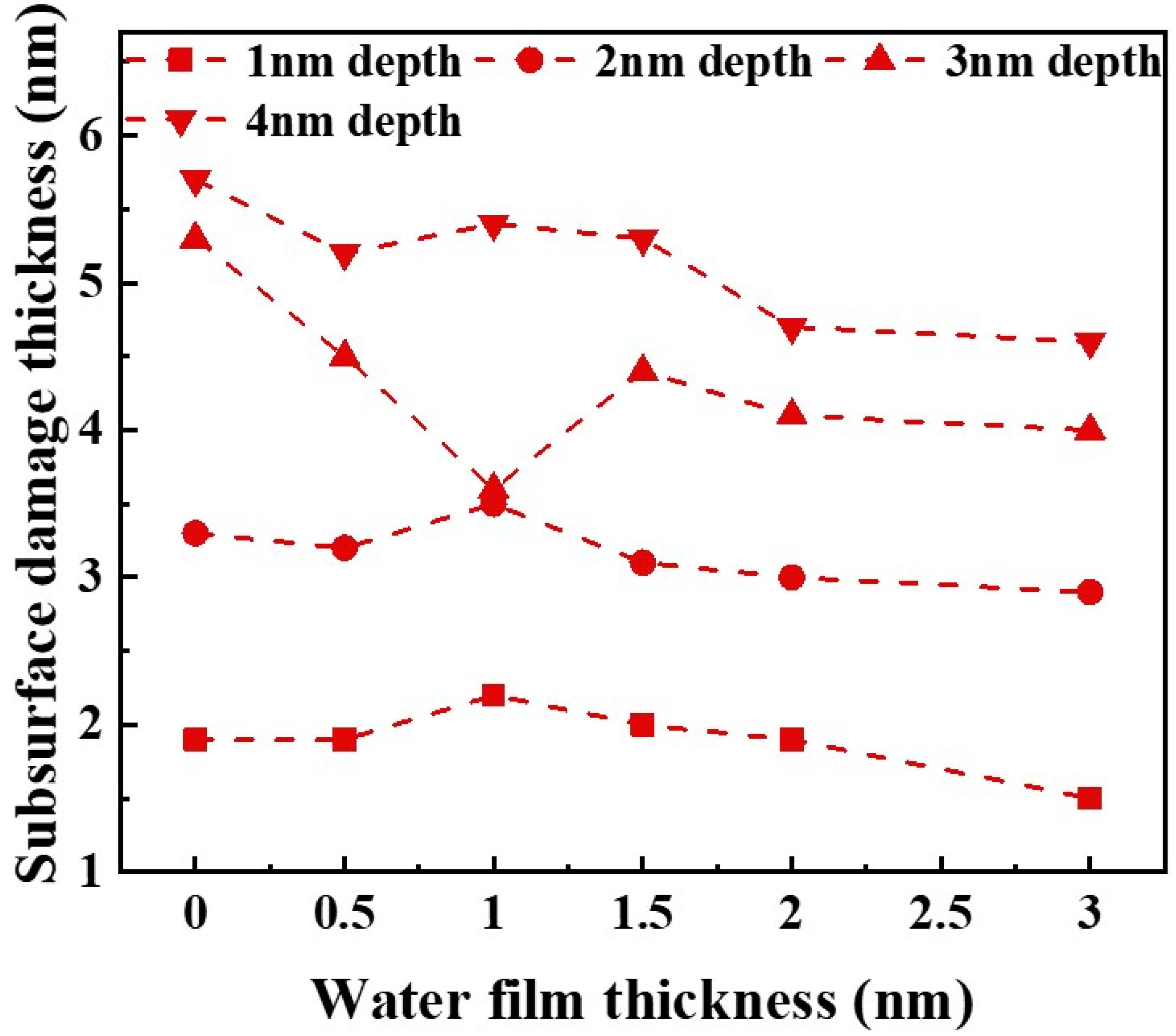
3.3. Subsurface Lattice Damage

In addition to surface nanotribological properties, subsurface lattice damage is also an important aspect during ultra-precision surface processing for hard-brittle semiconductor materials. Figure 9 illustrates the cross-section morphology and structural features after performing scratching with 2 nm scratching depth. The IDS analysis result suggests that after scratching, a part of the hexagonal wurtzite structure was transformed into an amorphous structure, and a small portion was transformed into a cubic diamond structure that was the zinc-blende lattice structure of GaN. Water film presence influenced the phase transition of GaN to a certain extent. Some water molecules flowed into the grooves, and some were adsorbed onto the diamond abrasive, thus reducing the direct contact between the diamond abrasive and the GaN workpiece during scratching. As the thickness of the water film increased, the more intensive resistance of the water film caused the workpiece to be subjected to a greater tangential force, in turn promoting the damage to the GaN workpiece. In addition, the water molecules in front of the diamond abrasive can alleviate the formation of wear debris during scratching.
To further evaluate the role of the water film in amorphization transition, we quantified the count of amorphous atoms under different conditions. Figure 10a–d show the change in the count of amorphous atoms as a function of scratching distance for different scratching depths. Both the scratching depth and the water film thickness exhibited an influence on the structural damage in the subsurface during scratching. With the advance of the diamond abrasive, the number of amorphous atoms gradually increased for various scratching depths, and the water film thickness increased as a whole. The number of amorphous atoms for the GaN workpiece covered with water film was higher than that for the bare GaN workpiece for all the selected conditions except the case of 1 nm water film thickness. Figure 11 shows the number of amorphous atoms versus water film thickness for the different scratching depths of 1, 2, 3, and 4 nm. There was no obvious functional relationship between the number of amorphous atoms and water film thickness. Increasing water film thickness would, to some extent, lead to more serious amorphization, except for the case of the 1 nm scratching depth. When the thickness of the water film was 1 nm, under the given scratch depth condition, the number of amorphous atoms was the least. This was because within a certain thickness, the water film mainly plays a lubricating role, effectively reducing the friction coefficient of the GaN surface. However, as the thickness of the water film increases, the inhibitory effect of the water film on friction gradually strengthens. The tangential force increases accordingly, generating more amorphous atoms. This also shows that, under certain conditions, the water film had a certain anti-wear effect on GaN, and the effect was most obvious when the thickness of the water film was 1 nm.
The friction between the diamond abrasive and the GaN workpiece can lead to an increase in the temperature in the scratching local region, resulting in a decrease in the hardness of the GaN crystal. As a result, the plastic deformation and removal of material were more likely to occur [35,36]. Meanwhile, the water film can act as a cooling heat sink to absorb heat in the scratching process of the water-film-covered GaN workpiece. The effect of the water molecule film on the temperature features during the scratching of the GaN workpiece should be classified to further indicate the role of the water film. Figure 12 displays the temperature distribution of the GaN workpieces with different water film thicknesses after scratching. It should be noted that the diamond abrasive in this study was treated as a rigid body and thus lost its heat conduction capability, meaning it could not absorb heat from the GaN workpiece in the scratching process. Consequently, the temperature distribution of the GaN workpiece shown in Figure 12 may deviate from the real condition under which diamond exhibits high thermal conductivity. In future work, we will attempt to establish a non-rigid diamond abrasive model to investigate the interactive behavior between diamond abrasives and GaN workpieces during nanoscratching. This will provide deeper insights into the deformation, wear, and heat absorption effects of GaN crystal, as well as their impacts on nanoscale to atomic scale material removal and damage mechanisms.
Compared to the dry friction of the GaN workpiece, the absorbed water film can quickly absorb partial-friction-induced heat and reduce the temperature of the GaN workpiece during the scratching process of the water-film-covered GaN workpiece, thus alleviating the material pile-up and structural damage of the GaN workpiece. Dislocations were primarily localized in front of the diamond abrasive and along the groove edges, with a few dislocations distributed within the groove region, as shown in Figure 13. Under dry friction conditions, the dislocations were concentrated near the grooves and were mainly located in front of the diamond abrasive. As the thickness of the water film increased, the development of the dislocations was more extensive, with more dislocations on both sides of the grooves. This is because the presence of the water film can cause the stress in front of the diamond abrasive to expand to both sides, thus resulting in the nucleation and development of dislocations on both sides of the groove. When the scratching depth was 1 nm, GaN crystals under dry friction conditions generated only a limited number of dislocations and minor plastic deformation, whereas inducing a water film can promote the formation of dislocations in the GaN crystals, as shown in Figure 14a. Moreover, the length of dislocation lines reached a maximum value at 0.5 nm water film thickness and decreased with the increase in the water film thickness. For the scratching depths of 2, 3, and 4 nm (see Figure 14b–d), the water film did not exhibit evident influence on the length of dislocation lines in GaN workpiece in total, but the maximum lengths of dislocation lines all occurred at the 1.5 nm water film thickness. Water film did not help inhibit the formation and development of dislocations during the scratching process with diamond abrasive.
Figure 15 illustrates the subsurface lattice damage induced by scratching for GaN workpieces with various water film thicknesses. It was observed that the damage layer thickness of GaN workpieces with water film was slightly smaller than that without water film, except in the case of 1 nm scratching depth. Also, there was no obvious difference in the subsurface damage among the above cases, indicating that the water film thickness did not influence the enhancement of subsurface quality. Figure 16 shows the variation in damage layer thickness within the subsurface as a function of water film thickness for various scratching depths. For the scratching depths of 3 and 4 nm, water films with each level of thickness can reduce the thickness of the damage layer. For 1 and 2 nm scratching depths, the damage layer thickness first increased and then decreased as the water film thickness rose, with the maximum thickness occurring at a water film thickness of 1 nm. These results suggest that the scratching-induced lattice damage can be alleviated only when using the high normal load at which severe plastic deformation occurred on the GaN workpiece.

4. Conclusions

MD simulations were employed to systematically investigate the influence of water molecular films with severe nanometer thickness on the nanotribological properties and subsurface lattice damage evolution of GaN surfaces during the nanoscratching process. The main conclusion can be summarised as follows:
(1)
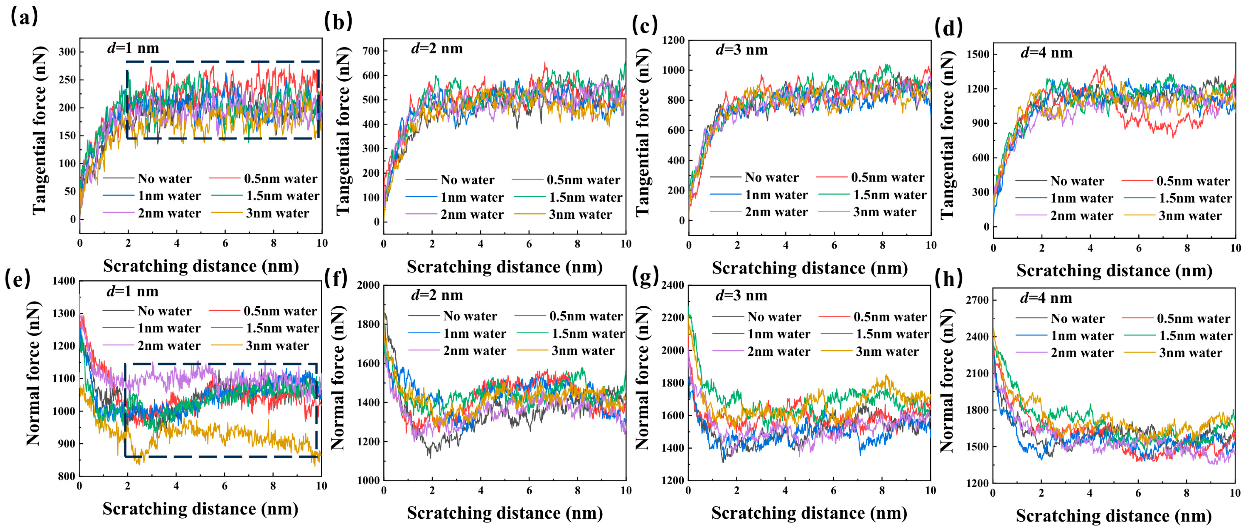
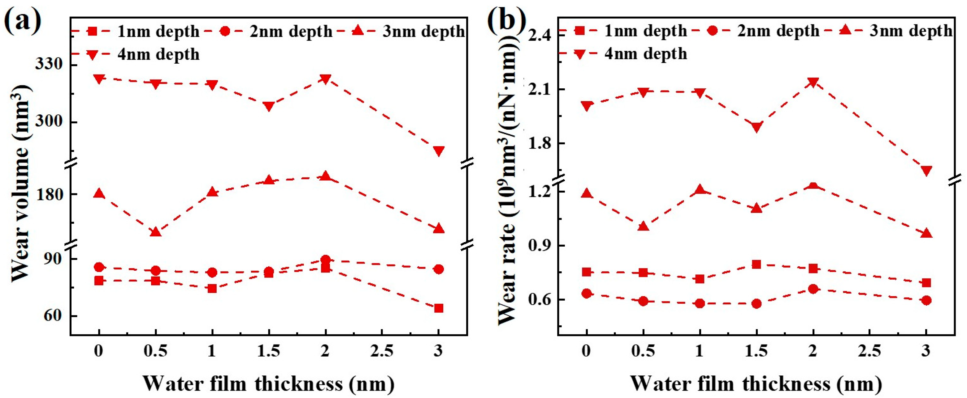
The tangential and normal forces exhibited no significant variation trend with increasing water film thickness from 0 to 3 nm, attributed to the competing effects of lubrication and movement obstruction of the water molecules during scratching. A 3 nm thick water film achieved the lowest friction coefficient under most scratching depth conditions. The water film influenced material plastic flow and chip formation, thereby mitigating the surface pile-up of GaN during scratching. In addition, the wear volume demonstrated a non-monotonic trend: it initially decreased, then increased, and subsequently decreased again as water film thickness rose from 0 to 3 nm, and it reached its minimum value at 3 nm water film thickness due to the enhanced lubrication and the heat absorption of the water film.
(2)
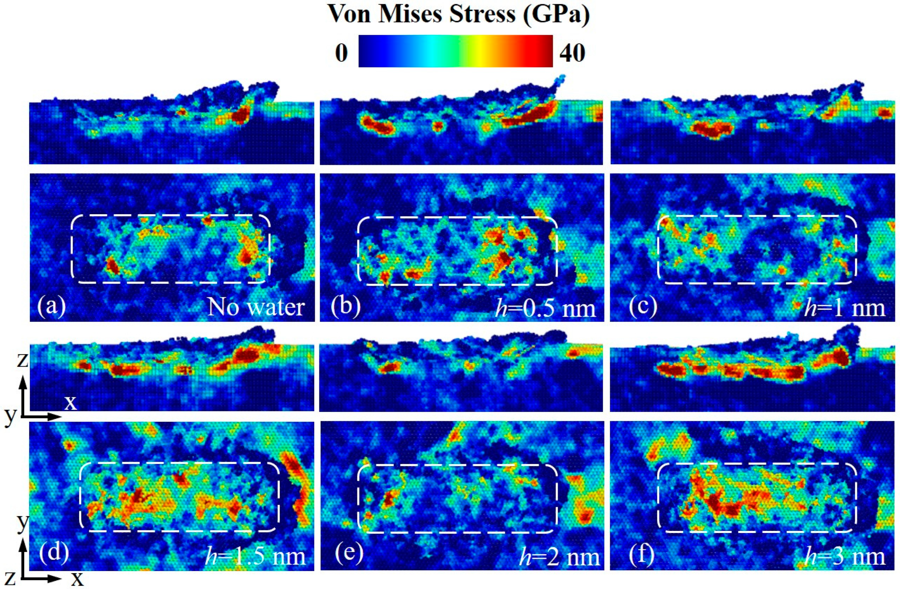
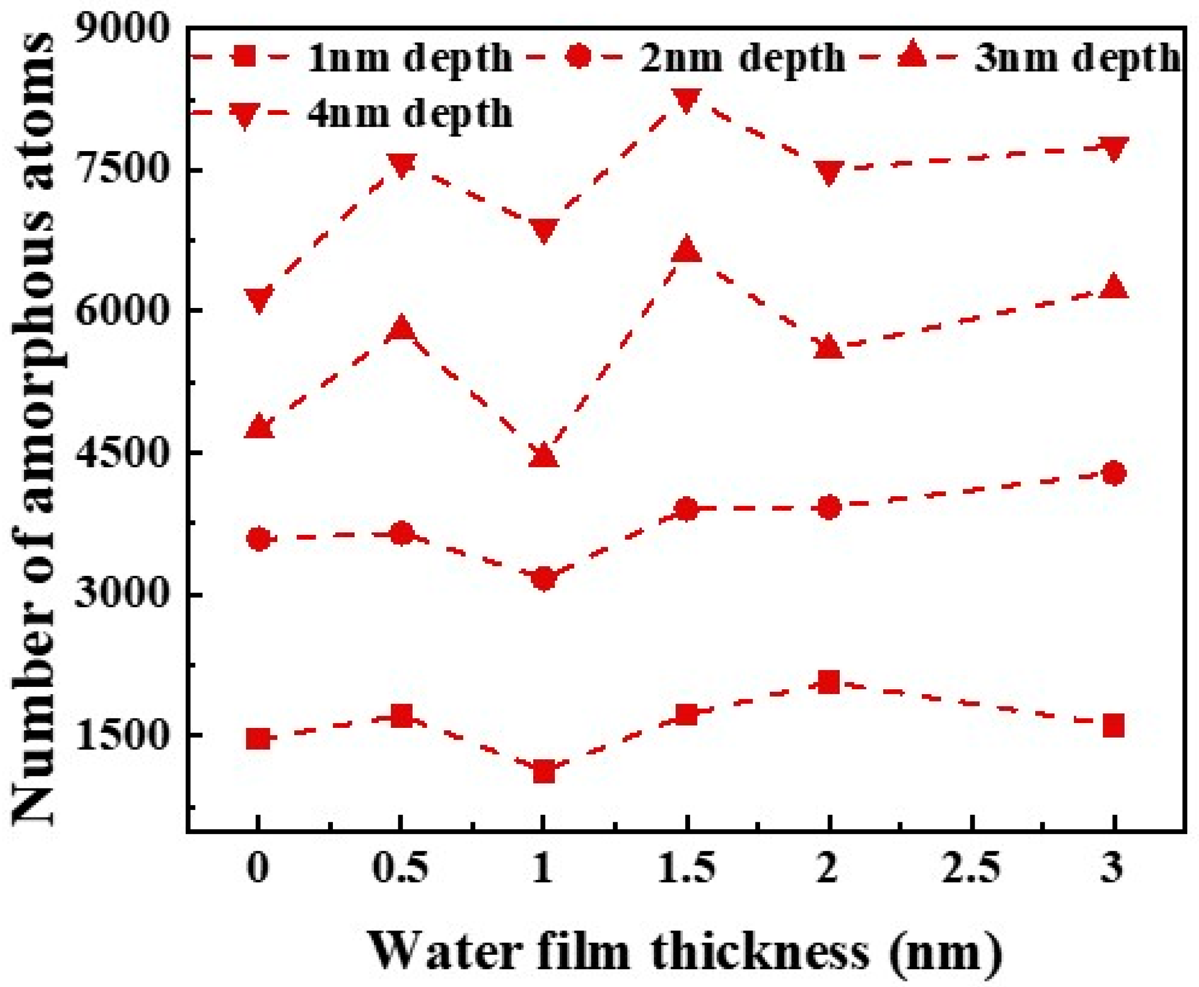
Water-film-covered GaN surfaces covered with water film exhibited a thinner subsurface damage layer compared to bare GaN workpiece, with the thickness of the damage layer monotonically decreasing as water film thickness increased. Nevertheless, the water film failed to inhibit the nucleation and propagation of the dislocations during scratching, and hence the water-film-covered GaN workpieces exhibited more dislocations than the bare GaN workpiece. This study can enhance the understanding of water film effects on the water-mediated nanotribological and ultra-precision machining processes of GaN.

Author Contributions

J.Y.: Conceptualization, investigation, data curation, formal analysis, writing—original draft. S.F.: investigation, data curation. Y.L.: investigation. J.G.: project administration, conceptualization, formal analysis, writing—review and editing, supervision, funding acquisition. All authors have read and agreed to the published version of the manuscript.

Funding

This research was funded by the National Natural Science Foundation of China (no. 51805240) and the Natural Science Foundation of Hunan Province (no. 2023JJ30514).

Data Availability Statement

All data generated or analyzed during this study are included in this published article.

Acknowledgments

The authors would like to acknowledge the National Natural Science Foundation of China (no. 51805240), the Natural Science Foundation of Hunan Province (no. 2023JJ30514), the Scientific Research Foundation of University of South China for the financial support, and the HPC Center of the University of South China for running the LAMMPS (Version 12 Dec 2018) software.

Conflicts of Interest

The authors declare that they have no known competing financial interests or personal relationships that could have appeared to influence the work reported in this paper.

References

  1. Wheeler, J.M.; Niederberger, C.; Tessarek, C.; Christiansen, S.; Michler, J. Extraction of plasticity parameters of GaN with high temperature, in situ micro-compression. Int. J. Plast. 2013, 40, 140–151. [Google Scholar] [CrossRef]
  2. Oka, T. Recent development of vertical GaN power devices. Jpn. J. Appl. Phys. 2019, 58, SB0805. [Google Scholar] [CrossRef]
  3. Zhong, Y.; Zhang, J.; Wu, S.; Jia, L.; Yang, X.; Liu, Y.; Zhang, Y.; Sun, Q. A review on the GaN-on-Si power electronic devices. Fundam. Res. 2022, 2, 462–475. [Google Scholar] [CrossRef] [PubMed]
  4. Sun, R.; Lai, J.; Chen, W.; Zhang, B. GaN Power Integration for High Frequency and High Efficiency Power Applications: A Review. IEEE Access 2020, 8, 15529–15542. [Google Scholar] [CrossRef]
  5. Wang, Y.; Hu, X.; Ge, L.; Liu, Z.; Xu, M.; Peng, Y.; Li, B.; Yang, Y.; Li, S.; Xie, X.; et al. Research Progress in Capping Diamond Growth on GaN HEMT: A Review. Crystals 2023, 13, 500. [Google Scholar] [CrossRef]
  6. Fletcher, A.S.A.; Nirmal, D. A survey of Gallium Nitride HEMT for RF and high power applications. Superlattices Microstruct. 2017, 109, 519–537. [Google Scholar] [CrossRef]
  7. Gao, S.; Huang, H.; Zhu, X.; Kang, R. Surface integrity and removal mechanism of silicon wafers in chemo-mechanical grinding using a newly developed soft abrasive grinding wheel. Mater. Sci. Semicond. Process. 2017, 63, 97–106. [Google Scholar] [CrossRef]
  8. Mori, Y.; Imanishi, M.; Murakami, K.; Yoshimura, M. Recent progress of Na-flux method for GaN crystal growth. Jpn. J. Appl. Phys. 2019, 58, SC0803. [Google Scholar] [CrossRef]
  9. Zhang, C.; Dong, Z.; Yuan, S.; Guo, X.; Kang, R.; Guo, D. Study on subsurface damage mechanism of gallium nitride in nano-grinding. Mater. Sci. Semicond. Process. 2021, 128, 105760. [Google Scholar] [CrossRef]
  10. Guo, J.; Chen, J.; Lin, Y.; Liu, Z.; Wang, Y. Effects of surface texturing on nanotribological properties and subsurface damage of monocrystalline GaN subjected to scratching investigated using molecular dynamics simulation. Appl. Surf. Sci. 2021, 539, 148277. [Google Scholar] [CrossRef]
  11. Xu, X.; Vaudo, R.P.; Brandes, G.R. Fabrication of GaN wafers for electronic and optoelectronic devices. Opt. Mater. 2003, 23, 1–5. [Google Scholar] [CrossRef]
  12. Weyher, J.L.; Müller, S.; Grzegory, I.; Porowski, S. Chemical polishing of bulk and epitaxial GaN. J. Cryst. Growth 1997, 182, 17–22. [Google Scholar] [CrossRef]
  13. Lee, J.; Kim, J.C.; Kim, J.; Singh, R.K.; Arjunan, A.C.; Lee, H. Evaluation of subsurface damage inherent to polished GaN substrates using depth-resolved cathodoluminescence spectroscopy. Thin Solid Film. 2018, 660, 516–520. [Google Scholar] [CrossRef]
  14. Zhou, P.; Li, J.; Wang, Z.; Chen, J.; Li, X.; Zhu, Y. Molecular dynamics study of the removal mechanism of SiC in a fixed abrasive polishing in water lubrication. Ceram. Int. 2020, 46, 24961–24974. [Google Scholar] [CrossRef]
  15. Wang, Y.; Zhu, Y.; Zhao, D.; Bian, D. Nanoscratch of aluminum in dry, water and aqueous H2O2 conditions. Appl. Surf. Sci. 2019, 464, 229–235. [Google Scholar] [CrossRef]
  16. Chen, X.; Zhao, Y.; Wang, Y.; Zhou, H.; Ni, Z.; An, W. Nanoscale friction and wear properties of silicon wafer under different lubrication conditions. Appl. Surf. Sci. 2013, 282, 25–31. [Google Scholar] [CrossRef]
  17. Goel, S.; Knaggs, M.; Goel, G.; Zhou, X.W.; Upadhyaya, H.M.; Thakur, V.K.; Kumar, V.; Bizarri, G.; Tiwari, A.; Murphy, A.; et al. Horizons of modern molecular dynamics simulation in digitalized solid freeform fabrication with advanced materials. Mater. Today Chem. 2020, 18, 100356. [Google Scholar] [CrossRef]
  18. Liang, L.; Li, S.; Chai, P.; Lan, K.; Yu, R. Molecular Dynamics Simulation of Single-Crystal 4H-SiC Nano Scratching with Different Scratching Directions of the Tool. Crystals 2023, 13, 1044. [Google Scholar] [CrossRef]
  19. Goel, S.; Luo, X.; Agrawal, A.; Reuben, R.L. Diamond machining of silicon: A review of advances in molecular dynamics simulation. Int. J. Mach. Tools Manuf. 2015, 88, 131–164. [Google Scholar] [CrossRef]
  20. Zhou, Q.; Jiao, Z.; Huang, Z.; Shi, Y.; Li, Y.; Yin, C.; Wang, H.; Pinto, H.C.; Greiner, C.; Liu, W. Wear-resistant CrCoNi nanocrystalline film via friction-driven surface segregation. Acta Mater. 2024, 279, 120299. [Google Scholar] [CrossRef]
  21. Jiao, Z.; Dong, Y.; Li, Q.; Zhou, Q.; Han, S.; Yin, C.; Huang, Z.; Wang, X.; Wang, H.; Liu, W. Enhancing tribocorrosion resistance of VCoNi alloys in artificial seawater via nitrogen alloying. Corros. Sci. 2025, 243, 112600. [Google Scholar] [CrossRef]
  22. Tian, Y.; Feng, H.; Li, J.; Fang, Q.; Zhang, L. Nanoscale sliding friction behavior on Cu/Ag bilayers influenced by water film. Appl. Surf. Sci. 2021, 545, 148957. [Google Scholar] [CrossRef]
  23. Zhou, Y.; Huang, Y.; Li, J.; Lv, W.; Zhu, F. Polishing process of 4H-SiC under different pressures in a water environment. Diam. Relat. Mater. 2023, 133, 109710. [Google Scholar] [CrossRef]
  24. Li, Z.; Yang, X.; Li, Y.; Yao, T. Molecular dynamics study of the effect of water lubrication three-body polishing sapphire. Mater. Today Commun. 2023, 36, 106396. [Google Scholar] [CrossRef]
  25. Wang, W.; Hua, D.; Zhou, Q.; Li, S.; Eder, S.J.; Shi, J.; Wang, Z.; Wang, H.; Liu, W. Effect of a water film on the material removal behavior of Invar during chemical mechanical polishing. Appl. Surf. Sci. 2023, 616, 156490. [Google Scholar] [CrossRef]
  26. Ren, J.; Zhao, J.; Dong, Z.; Liu, P. Molecular dynamics study on the mechanism of AFM-based nanoscratching process with water-layer lubrication. Appl. Surf. Sci. 2015, 346, 84–98. [Google Scholar] [CrossRef]
  27. Zhong, W.W.; Huang, Y.F.; Gan, D.; Xu, J.Y.; Li, H.; Wang, G.; Meng, S.; Chen, X.L. Wetting behavior of water on silicon carbide polar surfaces. Phys. Chem. Chem. Phys. 2016, 18, 28033–28039. [Google Scholar] [CrossRef]
  28. Gao, S.; Yang, L.H.; Gan, Y.; Chen, Q. The Influence of Sliding Speed on the Friction Behavior of Silica Surface. ACS Omega 2021, 6, 3384–3389. [Google Scholar] [CrossRef]
  29. Shi, J.; Chen, J.; Fang, L.; Sun, K.; Sun, J.; Han, J. Atomistic scale nanoscratching behavior of monocrystalline Cu influenced by water film in CMP process. Appl. Surf. Sci. 2018, 435, 983–992. [Google Scholar] [CrossRef]
  30. Béré, A.; Serra, A. On the atomic structures, mobility and interactions of extended defects in GaN: Dislocations, tilt and twin boundaries. Philos. Mag. 2006, 86, 2159–2192. [Google Scholar] [CrossRef]
  31. Qian, Y.; Deng, S.; Shang, F.; Wan, Q.; Yan, Y. Dependence of tribological behavior of GaN crystal on loading direction: A molecular dynamics study. J. Appl. Phys. 2019, 126, 075108. [Google Scholar] [CrossRef]
  32. Tian, Y.; Fang, Q.; Li, J. Molecular dynamics simulations for nanoindentation response of nanotwinned FeNiCrCoCu high entropy alloy. Nanotechnology 2020, 31, 465701. [Google Scholar] [CrossRef] [PubMed]
  33. Plimpton, S. Fast parallel algorithms for short-range molecular dynamics. J. Comput. Phys. 1995, 117, 1–19. [Google Scholar]
  34. Fang, Q.; Tian, Y.; Li, J.; Wang, Q.; Wu, H. Interface-governed nanometric machining behaviour of Cu/Ag bilayers using molecular dynamics simulation. RSC Adv. 2019, 9, 1341–1353. [Google Scholar] [PubMed]
  35. Li, J.; Fang, Q.; Zhang, L.; Liu, Y. The effect of rough surface on nanoscale high speed grinding by a molecular dynamics simulation. Comput. Mater. Sci. 2015, 98, 252–262. [Google Scholar] [CrossRef]
  36. Tohamey, Y.M.; Abdel Magied, A.M.; Salah El Din, L.A.; Mohamed, R.A. MRI is it complementary or mandatory to ultrasound in classification of different congenital anomalies of female reproductive tract? Egypt. J. Radiol. Nucl. Med. 2018, 49, 571–578. [Google Scholar] [CrossRef]
Figure 1. Molecular dynamics model of the water-film-covered GaN workpiece scratched by a single diamond abrasive.
Crystals 15 00428 g001
Figure 2. Nanoindentation morphology of GaN at the indentation depth of 2 nm for different thicknesses of water films. (a) Without water film; (b) 0.5 nm thick water film; (c) 1 nm thick water film; (d) 1.5 nm thick water film; (e) 2 nm thick water film; (f) 3 nm thick water film.
Crystals 15 00428 g002
Figure 3. Cross-sectional profiles at the indentation depth of 2 nm for different thicknesses of water films. (a) Without water film; (b) 0.5 nm thick water film; (c) 1 nm thick water film; (d) 1.5 nm thick water film; (e) 2 nm thick water film; (f) 3 nm thick water film. The top cloud maps are colored with the hydrostatic stress, and the atoms in the bottom figures are colored with their IDS types.
Crystals 15 00428 g003
Figure 4. Variation of (ad) tangential force and (eh) normal forces at three scratching depths for different water film thicknesses.
Crystals 15 00428 g004
Figure 5. Average scratching force versus water film thickness for different scratching depths. (a) d = 1 nm; (b) d = 2 nm; (c) d = 3 nm; and (d) d = 4 nm.
Crystals 15 00428 g005
Figure 6. Surface pile-up and morphology after scratching with a scratching depth of 2 nm for different water film thicknesses. (a) h = 0 nm (no water); (b) h = 0.5 nm; (c) h = 1 nm; (d) h = 1.5 nm; (e) h = 2 nm; (f) h = 3 nm.
Crystals 15 00428 g006
Figure 7. Von Mises stress distribution after abrasive withdrawal for different water film thicknesses. (a) h = 0 nm (no water); (b) h = 0.5 nm; (c) h = 1 nm; (d) h = 1.5 nm; (e) h = 2 nm; (f) h = 3 nm. The scratching depth was 2 nm.
Crystals 15 00428 g007
Figure 8. (a) Wear volume and (b) wear rate as a function of water film thickness at different scratching depths.
Crystals 15 00428 g008
Figure 9. Structural feature of GaN workpiece/water film after scratching with a scratching depth of 2 nm. (a) h = 0 nm (no water); (b) h = 0.5 nm; (c) h = 1 nm; (d) h = 1.5 nm; (e) h = 2 nm; (f) h = 3 nm.
Crystals 15 00428 g009
Figure 10. Variation of number of amorphous atoms with scratching distance for various scratching depths. (a) d = 1 nm; (b) d = 2 nm; (c) d = 3 nm; (d) d = 4 nm.
Crystals 15 00428 g010
Figure 11. Number of amorphous atoms versus water film thickness for different scratching depths.
Crystals 15 00428 g011
Figure 12. Temperature distribution of water-film-covered GaN workpieces with different water film thicknesses after scratching. (a) h = 0 nm (no water); (b) h = 0.5 nm; (c) h = 1 nm; (d) h = 1.5 nm; (e) h = 2 nm; (f) h = 3 nm. The scratching depth was 2 nm.
Crystals 15 00428 g012
Figure 13. Dislocation distribution in the GaN workpiece after scratching with a scratching depth of 2 nm. (a) h = 0 nm (no water); (b) h = 0.5 nm; (c) h = 1 nm; (d) h = 1.5 nm; (e) h = 2 nm; (f) h = 3 nm.
Crystals 15 00428 g013
Figure 14. The final length of dislocation lines after scratching for various scratching depths. (a) d = 1 nm; (b) d = 2 nm; (c) d = 3 nm; (d) d = 4 nm.
Crystals 15 00428 g014
Figure 15. Comparison of the scratching-induced subsurface damage of GaN workpieces for different water film thicknesses after scratching with a scratching depth of 2 nm. (a) h = 0 nm (no water); (b) h = 0.5 nm; (c) h = 1 nm; (d) h = 1.5 nm; (e) h = 2 nm; (f) h = 3 nm.
Crystals 15 00428 g015
Figure 16. Subsurface damage layer thickness for various water film thicknesses after scratching.
Crystals 15 00428 g016
Table 1. The MD simulation parameters.
Parameters NameValue
Radius of Diamond Abrasive, R (nm)4
Water filmDensity, ρ (g/cm3)1
Thickness, h (nm)0.5, 1, 1.5, 2, and 3
Size of GaN workpiece (nm3)30 × 20 × 15
Scratching depth, d (nm)1, 2, 3, and 4
Scratching distance, L (nm)10
Scratching velocity, v (m/s)40
Scratching direction[1-210] crystal orientation
Table 2. The values of the potentials employed in the MD simulation.
PotentialTypeParameters
GaNSW potentialRefs. [30,31]
C-N6-12 LJε = 0.0037235 eV, δ = 0.33677 nm
O-Ga6-12 LJε =0.0084843 eV, δ = 0.34721 nm
O-N6-12 LJε = 0.0037321 eV, δ = 0.31479 nm
O-C6-12 LJε = 0.0041369 eV, δ = 0.32531 nm
C-Ga6-12 LJε = 0.0084646 eV, δ = 0.36919 nm
O-O12-12 LJε = 0.0041499 eV, δ = 0.30332 nm
Disclaimer/Publisher’s Note: The statements, opinions and data contained in all publications are solely those of the individual author(s) and contributor(s) and not of MDPI and/or the editor(s). MDPI and/or the editor(s) disclaim responsibility for any injury to people or property resulting from any ideas, methods, instructions or products referred to in the content.

