
Recent Advancements in P-Type Inorganic Semiconductor Thin-Film Transistors: A Review


Abstract
1. Introduction
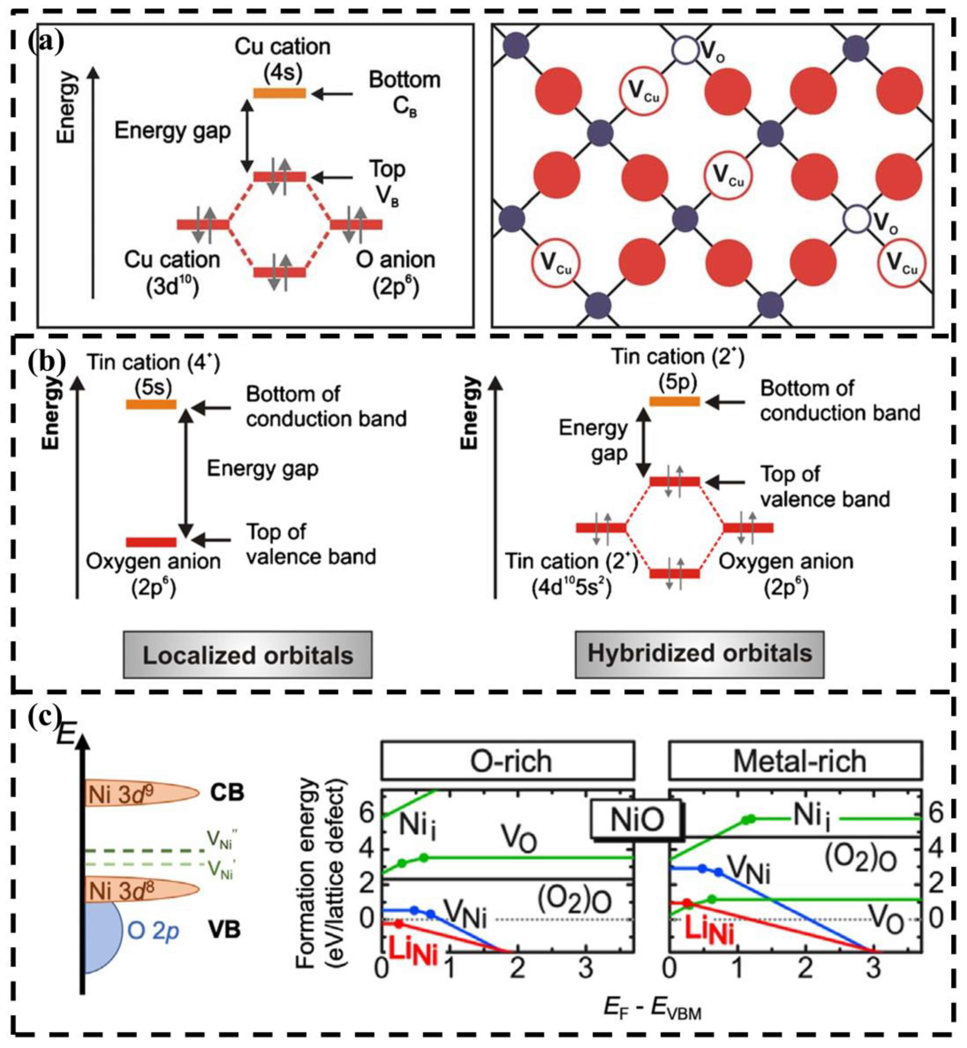
2. P-Type Semiconductor Materials
3. Advancements in P-Type Semiconductor Devices
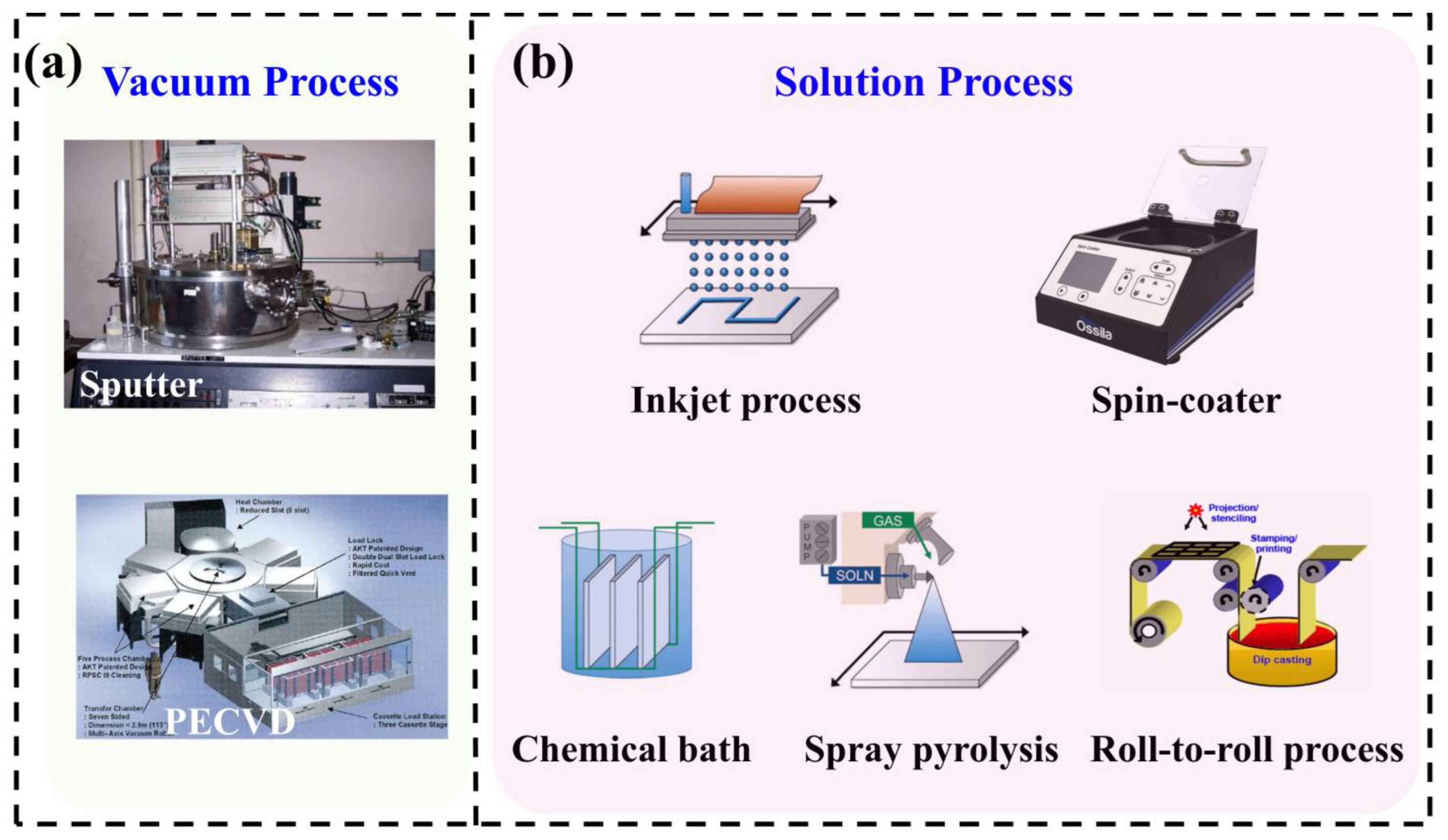
3.1. P-Type TFTs by Solution Process
3.2. Improvement in Organic P-Type Materials
3.3. Integration of Flexible Devices
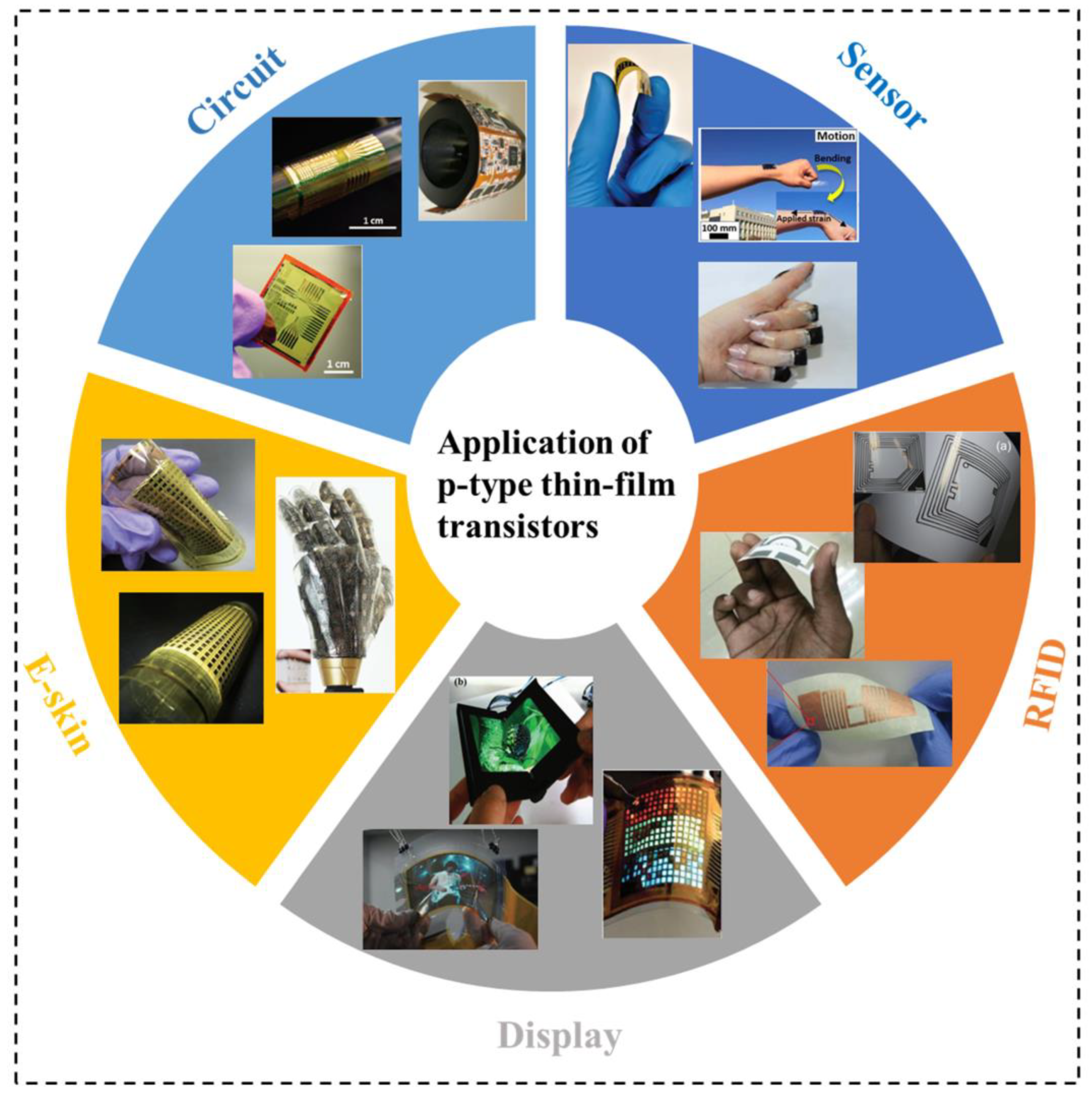
3.4. Application of P-Type Thin-Film Transistors
3.5. Challenges
4. Conclusions and Outlook
Author Contributions
Funding
Data Availability Statement
Conflicts of Interest
References
- Fortunato, E.; Barquinha, P.; Martins, R. Oxide Semiconductor Thin—Film Transistors: A Review of Recent Advances. Adv. Mater. 2012, 24, 2945–2986. [Google Scholar] [CrossRef] [PubMed]
- Wang, Z.; Nayak, P.K.; Caraveo-Frescas, J.A.; Alshareef, H.N. Recent Developments in P-Type Oxide Semiconductor Materials and Devices. Adv. Mater. 2016, 28, 3831–3892. [Google Scholar] [CrossRef] [PubMed]
- Cho, S.W.; Jo, C.; Kim, Y.-H.; Park, S.K. Progress of materials and devices for neuromorphic vision sensors. Nano-Micro Lett. 2022, 14, 203. [Google Scholar] [CrossRef]
- Nomura, K.; Ohta, H.; Takagi, A.; Kamiya, T.; Hirano, M.; Hosono, H. Room-Temperature Fabrication of Transparent Flexible Thin-Film Transistors Using Amorphous Oxide Semiconductors. Nature 2004, 432, 488–492. [Google Scholar] [CrossRef]
- Raebiger, H.; Lany, S.; Zunger, A. Origins of the p-type nature and cation deficiency in Cu2O and related materials. Phys. Rev. B 2007, 76, 045209. [Google Scholar] [CrossRef]
- Yim, K.; Youn, Y.; Lee, M.; Yoo, D.; Lee, J.; Cho, S.H.; Han, S. Computational Discovery of P-Type Transparent Oxide Semiconductors Using Hydrogen Descriptor. NPJ Comput. Mater. 2018, 4, 17. [Google Scholar] [CrossRef]
- Gao, W.; Ota, H.; Kiriya, D.; Takei, K.; Javey, A. Flexible Electronics toward Wearable Sensing. Acc. Chem. Res. 2019, 52, 523–533. [Google Scholar] [CrossRef]
- Lee, J.M.; Cho, S.W.; Jo, C.; Yang, S.H.; Kim, J.; Kim, D.Y.; Jo, J.-W.; Park, J.S.; Kim, Y.-H.; Park, S.K. Monolithically integrated neuromorphic electronic skin for biomimetic radiation shielding. Sci. Adv. 2024, 10, eadp9885. [Google Scholar] [CrossRef]
- Baumbauer, C.L.; Anderson, M.G.; Ting, J.; Sreekumar, A.; Rabaey, J.M.; Arias, A.C.; Thielens, A. Printed, Flexible, Compact UHF-RFID Sensor Tags Enabled by Hybrid Electronics. Sci. Rep. 2020, 10, 16543. [Google Scholar] [CrossRef]
- Ou, C.-W.; Dhananjay, D.; Ho, Z.Y.; Chuang, Y.-C.; Cheng, S.-S.; Wu, M.-C.; Ho, K.-C.; Chu, C.-W. Anomalous P-Channel Amorphous Oxide Transistors Based on Tin Oxide and Their Complementary Circuits. Appl. Phys. Lett. 2008, 92, 122113. [Google Scholar] [CrossRef]
- Dhananjay, D.; Chu, C.-W.; Ou, C.-W.; Wu, M.-C.; Ho, Z.-Y.; Ho, K.-C.; Lee, S.-W. Complementary Inverter Circuits Based on P-SnO2 and n-In2O3 Thin Film Transistors. Appl. Phys. Lett. 2008, 92, 232103. [Google Scholar] [CrossRef]
- Lee, H.-N.; Kim, H.-J.; Kim, C.-K. P-Channel Tin Monoxide Thin Film Transistor Fabricated by Vacuum Thermal Evaporation. Jpn. J. Appl. Phys. 2010, 49, 020202. [Google Scholar] [CrossRef]
- Liang, L.Y.; Liu, Z.M.; Cao, H.T.; Yu, Z.; Shi, Y.Y.; Chen, A.H.; Zhang, H.Z.; Fang, Y.Q.; Sun, X.L. Phase and Optical Characterizations of Annealed SnO Thin Films and Their P-Type TFT Application. J. Electrochem. Soc. 2010, 157, H598. [Google Scholar] [CrossRef]
- Kim, S.H.; Baek, I.-H.; Kim, D.H.; Pyeon, J.J.; Chung, T.-M.; Baek, S.-H.; Kim, J.-S.; Han, J.H.; Kim, S.K. Fabrication of High-Performance p-Type Thin Film Transistors Using Atomic-Layer-Deposited SnO Films. J. Mater. Chem. C 2017, 5, 3139–3145. [Google Scholar] [CrossRef]
- Yabuta, H.; Nomura, K.; Kaji, N.; Kumomi, H.; Hayashi, R.; Hirano, M.; Kamiya, T.; Hosono, H. Sputtering Formation of P-Type SnO Thin-Film Transistors on Glass toward Oxide Complimentary Circuits. Appl. Phys. Lett. 2010, 97, 072111. [Google Scholar] [CrossRef]
- Zhang, Y.; He, G.; Wang, L.; Wang, W.; Xu, X.; Liu, W. Ultraviolet-Assisted Low-Thermal-Budget-Driven α-InGaZnO Thin Films for High-Performance Transistors and Logic Circuits. ACS Nano 2022, 16, 4961–4971. [Google Scholar] [CrossRef]
- Thomas, S.R.; Pattanasattayavong, P.; Anthopoulos, T.D. Solution-Processable Metal Oxide Semiconductors for Thin-Film Transistor Applications. Chem. Soc. Rev. 2013, 42, 6910. [Google Scholar] [CrossRef]
- Yu, X.; Marks, T.J.; Facchetti, A. Metal Oxides for Optoelectronic Applications. Nat. Mater. 2016, 15, 383–396. [Google Scholar] [CrossRef]
- Kim, D.; Liu, Z.; Kim, Y.; Wu, J.; Song, J.; Kim, H.; Huang, Y.; Hwang, K.; Zhang, Y.; Rogers, J.A. Optimized Structural Designs for Stretchable Silicon Integrated Circuits. Small 2009, 5, 2841–2847. [Google Scholar] [CrossRef]
- Sun, Y.; Choi, W.M.; Jiang, H.; Huang, Y.Y.; Rogers, J.A. Controlled Buckling of Semiconductor Nanoribbons for Stretchable Electronics. Nat. Nanotechnol. 2006, 1, 201–207. [Google Scholar] [CrossRef]
- Fortunato, E.; Figueiredo, V.; Barquinha, P.; Elamurugu, E.; Barros, R.; Gonçalves, G.; Park, S.-H.K.; Hwang, C.-S.; Martins, R. Thin-Film Transistors Based on p-Type Cu2O Thin Films Produced at Room Temperature. Appl. Phys. Lett. 2010, 96, 192102. [Google Scholar] [CrossRef]
- Scanlon, D.O.; Morgan, B.J.; Walsh, A.; Watson, G.W. Acceptor Levels In p-Type Cu2O: Rationalizing Theory and Experiment. Phys. Rev. Lett. 2009, 103, 096405. [Google Scholar] [CrossRef] [PubMed]
- Scanlon, D.O.; Watson, G.W. Understanding the P-Type Defect Chemistry of CuCrO2. J. Mater. Chem. 2011, 21, 3655. [Google Scholar] [CrossRef]
- Fortunato, E.; Barros, R.; Barquinha, P.; Figueiredo, V.; Park, S.-H.K.; Hwang, C.-S.; Martins, R. Transparent P-Type SnOx Thin Film Transistors Produced by Reactive Rf Magnetron Sputtering Followed by Low Temperature Annealing. Appl. Phys. Lett. 2010, 97, 052105. [Google Scholar] [CrossRef]
- Greiner, M.T.; Helander, M.G.; Tang, W.-M.; Wang, Z.-B.; Qiu, J.; Lu, Z.-H. Universal Energy-Level Alignment of Molecules on Metal Oxides. Nat. Mater. 2011, 11, 76–81. [Google Scholar] [CrossRef]
- Napari, M.; Huq, T.N.; Hoye, R.L.Z.; Macmanus-Driscoll, J.L. Nickel Oxide Thin Films Grown by Chemical Deposition Techniques: Potential and Challenges in Next-generation Rigid and Flexible Device Applications. InfoMat 2020, 3, 536–576. [Google Scholar] [CrossRef]
- Lany, S.; Osorio-Guillén, J.; Zunger, A. Origins of the Doping Asymmetry in Oxides: Hole Doping in NiO versus Electron Doping in ZnO. Phys. Rev. B 2007, 75, 241203. [Google Scholar] [CrossRef]
- Nachman, M.; Cojocaru, L.N.; Rîbco, L.V. Electrical Properties of Non-Stoichiometric Nickel Oxide. Phys. Status Solid B 1965, 8, 773–783. [Google Scholar] [CrossRef]
- Zhang, J.Y.; Li, W.W.; Hoye, R.L.Z.; Macmanus-Driscoll, J.L.; Budde, M.; Bierwagen, O.; Wang, L.; Du, Y.; Wahila, M.J.; Piper, L.F.J.; et al. Electronic and Transport Properties of Li-Doped NiO Epitaxial Thin Films. J. Mater. Chem. C 2018, 6, 2275–2282. [Google Scholar] [CrossRef]
- Sawatzky, G.A.; Allen, J.W. Magnitude and Origin of the Band Gap in NiO. Phys. Rev. Lett. 1984, 53, 2339–2342. [Google Scholar] [CrossRef]
- Dare-Edwards, M.P.; Goodenough, J.B.; Hamnett, A.; Nickolson, N.D. Photoelectrochemistry of nickel (II) oxide. J. Chem. Soc. Faraday Trans. 1981, 77, 643–661. [Google Scholar]
- Taguchi, M.; Matsunami, M.; Ishida, Y.; Eguchi, R.; Chainani, A.; Takata, Y.; Yabashi, M.; Tamasaku, K.; Nishino, Y.; Ishikawa, T.; et al. Revisiting the Valence-Band and Core-Level Photoemission Spectra of NiO. Phys. Rev. Lett. 2008, 100, 206401. [Google Scholar] [CrossRef] [PubMed]
- Fingerle, M.; Tengeler, S.; Calvet, W.; Jaegermann, W.; Mayer, T. Sputtered Nickel Oxide Thin Films on N-Si(100)/SiO2 Surfaces for Photo-Electrochemical Oxygen Evolution Reaction (OER): Impact of Deposition Temperature on OER Performance and on Composition before and after OER. J. Electrochem. Soc. 2020, 167, 136514. [Google Scholar] [CrossRef]
- Okamura, K.; Nasr, B.; Brand, R.A.; Hahn, H. Solution-Processed Oxide Semiconductor SnO in p-Channel Thin-Film Transistors. J. Mater. Chem. C 2012, 22, 4607. [Google Scholar] [CrossRef]
- Pattanasattayavong, P.; Yaacobi-Gross, N.; Zhao, K.; Ndjawa, G.O.N.; Li, J.; Yan, F.; O’Regan, B.C.; Amassian, A.; Anthopoulos, T.D. Hole-Transporting Transistors and Circuits Based on the Transparent Inorganic Semiconductor Copper(I) Thiocyanate (CuSCN) Processed from Solution at Room Temperature. Adv. Mater. 2013, 25, 1504–1509. [Google Scholar] [CrossRef]
- Pattanasattayavong, P.; Thomas, S.; Adamopoulos, G.; Mclachlan, M.A.; Anthopoulos, T.D. p-Channel Thin-Film Transistors Based on Spray-Coated Cu2O Films. Appl. Phys. Lett. 2013, 102, 163505. [Google Scholar] [CrossRef]
- Kim, S.Y.; Ahn, C.H.; Lee, J.Y.; Kwon, Y.H.; Hwang, S.; Lee, J.Y.; Cho, H.K. P-Channel Oxide Thin Film Transistors Using Solution-Processed Copper Oxide. ACS Appl. Mater. Interfaces 2013, 5, 2417–2421. [Google Scholar] [CrossRef]
- Mukhopadhyaya, K.; Srividya, P. Challenges in P-Type Oxide Based Thin Film Transistor. In IOP Conference Series: Materials Science and Engineering; IOP Publishing Ltd: Bristol, UK, 2020; Volume 1012, p. 012055. [Google Scholar] [CrossRef]
- Yu, J.; Liu, G.; Liu, A.; Meng, Y.; Shin, B.; Shan, F. Solution-Processed p-Type Copper Oxide Thin-Film Transistors Fabricated by Using a One-Step Vacuum Annealing Technique. J. Mater. Chem. C 2015, 3, 9509–9513. [Google Scholar] [CrossRef]
- Choi, C.-H.; Gorecki, J.Y.; Fang, Z.; Allen, M.; Li, S.; Lin, L.-Y.; Cheng, C.-C.; Chang, C.-H. Low-Temperature, Inkjet Printed p-Type Copper(i) Iodide Thin Film Transistors. J. Mater. Chem. C 2016, 4, 10309–10314. [Google Scholar] [CrossRef]
- Liu, A.; Liu, G.; Zhu, H.; Shin, B.; Fortunato, E.; Martins, R.; Shan, F. Hole Mobility Modulation of Solution-Processed Nickel Oxide Thin-Film Transistor Based on High-k Dielectric. Appl. Phys. Lett. 2016, 108, 233506. [Google Scholar] [CrossRef]
- Jang, J.; Chung, S.; Kang, H.; Subramanian, V. P-Type CuO and Cu2O Transistors Derived from a Sol–Gel Copper (II) Acetate Monohydrate Precursor. Thin Solid Films 2016, 600, 157–161. [Google Scholar] [CrossRef]
- Li, Y.; Liu, C.; Wang, G.; Pei, Y. Investigation of Solution Combustion-Processed Nickel Oxide p-Channel Thin Film Transistors. Semicond. Sci. Technol. 2017, 32, 085004. [Google Scholar] [CrossRef]
- Liu, A.; Nie, S.; Liu, G.; Zhu, H.; Zhu, C.; Shin, B.; Fortunato, E.; Martins, R.; Shan, F. In Situ One-Step Synthesis of p-Type Copper Oxide for Low-Temperature, Solution-Processed Thin-Film Transistors. J. Mater. Chem. C 2017, 5, 2524–2530. [Google Scholar] [CrossRef]
- Hu, H.; Zhu, J.; Chen, M.; Guo, T.; Li, F. Inkjet-Printed p-Type Nickel Oxide Thin-Film Transistor. Appl. Surf. Sci. 2018, 441, 295–302. [Google Scholar] [CrossRef]
- Jung, T.S.; Lee, H.; Park, S.P.; Kim, H.J.; Lee, J.H.; Kim, D.; Kim, H.J. Enhancement of Switching Characteristic for P-Type Oxide Semiconductors Using Hypochlorous Acid. ACS Appl. Mater. Interfaces 2018, 10, 32337–32343. [Google Scholar] [CrossRef]
- Pasquarelli, R.M.; Ginley, D.S.; O’Hayre, R. Solution Processing of Transparent Conductors: From Flask to Film. Chem. Soc. Rev. 2011, 40, 5406. [Google Scholar] [CrossRef]
- Mude, N.N.; Bukke, R.N.; Jang, J. Solution-Processed High-Performance p-Channel Copper Tin Sulfide Thin-Film Transistors. J. Mater. Chem. C 2021, 9, 9188–9196. [Google Scholar] [CrossRef]
- Mude, N.N.; Bukke, R.N.; Jang, J. High Performance of Solution-Processed Amorphous p-Channel Copper-Tin-Sulfur-Gallium Oxide Thin-Film Transistors by UV/O3 Photocuring. ACS Appl. Mater. Interfaces 2021, 13, 20277–20287. [Google Scholar] [CrossRef]
- Cheng, X.; Lu, B.; Lu, J.; Li, S.; Lu, R.; Yue, S.; Chen, L.; Ye, Z. Amorphous P-Type CuNiSnO Thin-Film Transistors Processed at Low Temperatures. IEEE Trans. Electron Devices 2020, 67, 2336–2341. [Google Scholar] [CrossRef]
- Wijeyasinghe, N.; Eisner, F.; Tsetseris, L.; Tessler, N.; Lin, Y.; Seitkhan, A.; Li, J.; Yan, F.; Solomeshch, O.; Tessler, N.; et al. P-Doping of Copper(I) Thiocyanate (CuSCN) Hole-Transport Layers for High-Performance Transistors and Organic Solar Cells. Adv. Funct. Mater. 2018, 28, 1802055. [Google Scholar] [CrossRef]
- Lu, S.; Smith, B.N.; Meikle, H.; Therien, M.J.; Franklin, A.D. All-Carbon Thin-Film Transistors Using Water-Only Printing. Nano Lett. 2023, 23, 2100–2106. [Google Scholar] [CrossRef] [PubMed]
- Petti, L.; Pattanasattayavong, P.; Lin, Y.-H.; Münzenrieder, N.; Cantarella, G.; Yaacobi-Gross, N.; Yan, F.; Tröster, G.; Anthopoulos, T.D. Solution-Processed p-Type Copper(I) Thiocyanate (CuSCN) for Low-Voltage Flexible Thin-Film Transistors and Integrated Inverter Circuits. Appl. Phys. Lett. 2017, 110, 113504. [Google Scholar] [CrossRef]
- Ji, Y.; Lee, H.J.; Lee, S.; Cho, K.G.; Lee, K.H.; Hong, K. High-Performance P-Type Copper(I) Thiocyanate Thin Film Transistors Processed from Solution at Low Temperature. Adv. Mater. Interfaces 2019, 6, 1900883. [Google Scholar] [CrossRef]
- Ka, I.; Gerlein, L.F.; Asuo, I.M.; Bouzidi, S.; Gedamu, D.M.; Pignolet, A.; Rosei, F.; Nechache, R.; Cloutier, S.G. Solution-Processed p-Type Copper Thiocyanate (CuSCN) Enhanced Sensitivity of PbS-Quantum-Dots-Based Photodiode. ACS Photonics 2020, 7, 1628–1635. [Google Scholar] [CrossRef]
- Liu, A.; Zhu, H.; Guo, Z.; Meng, Y.; Liu, G.; Fortunato, E.; Martins, R.; Shan, F. Solution Combustion Synthesis: Low-Temperature Processing for p-Type Cu:NiO Thin Films for Transparent Electronics. Adv. Mater. 2017, 29, 1701599. [Google Scholar] [CrossRef]
- Yang, J.; Wang, B.; Zhang, Y.; Ding, X.; Zhang, J. Low-temperature combustion synthesis and UV treatment processed p-type Li:NiOx active semiconductors for high-performance electronics. J. Mater. Chem. C 2018, 6, 12584–12591. [Google Scholar] [CrossRef]
- Wu, H.; Liang, L.; Wang, X.; Shi, X.; Zhang, H.; Pei, Y.; Li, W.; Sun, B.; Shen, C.; Cao, H. High-mobility flexible/transparent p-type copper iodide thin-film transistors and complementary inverters. Appl. Surf. Sci. 2023, 612, 155795. [Google Scholar] [CrossRef]
- Kim, H.-M.; Lee, W.-B.; Koo, H.; Kim, S.-Y.; Park, J.-S. Controlled 2D Growth Approach via Atomic Layer Deposition for Improved Stability and Performance in Flexible SnO Thin-Film Transistors. J. Mater. Chem. C 2024, 12, 8390–8397. [Google Scholar] [CrossRef]
- Liu, S.; Liu, R.; Chen, Y.; Ho, S.; Kim, J.H.; So, F. Nickel Oxide Hole Injection/Transport Layers for Efficient Solution-Processed Organic Light-Emitting Diodes. Chem. Mater. 2014, 26, 4528–4534. [Google Scholar] [CrossRef]
- Lin, T.; Li, X.; Jang, J. High Performance P-Type NiOx Thin-Film Transistor by Sn Doping. Appl. Phys. Lett. 2016, 108, 233503. [Google Scholar] [CrossRef]
- Daus, A.; Han, S.; Knobelspies, S.; Cantarella, G.; Troster, G. Ge2Sb2Te5 P-Type Thin-Film Transistors on Flexible Plastic Foil. Materials 2018, 11, 1672. [Google Scholar] [CrossRef] [PubMed]
- Shijeesh, M.R.; Jayaraj, M.K. Low Temperature Fabrication of CuxO Thin-Film Transistors and Investigation on the Origin of Low Field Effect Mobility. J. Appl. Phys. 2017, 123, 161538. [Google Scholar] [CrossRef]
- Liu, A.; Zhu, H.; Park, W.-T.; Kang, S.-J.; Xu, Y.; Kim, M.-G.; Noh, Y.-Y. Room-Temperature Solution-Synthesized p-Type Copper(I) Iodide Semiconductors for Transparent Thin-Film Transistors and Complementary Electronics. Adv. Mater. 2018, 30, 1802379. [Google Scholar] [CrossRef] [PubMed]
- Zhu, H.; Noh, Y.-Y.; Liu, A. Impact of Humidity on the Performance and Stability of Solution-Processed Copper Oxide Transistors. IEEE Electron Device Lett. 2020, 41, 1033–1035. [Google Scholar] [CrossRef]
- Bae, J.H.; Lee, J.H.; Park, S.P.; Jung, T.S.; Kim, H.J.; Kim, D.; Lee, S.-W.; Park, K.-S.; Yoon, S.; Kang, I.; et al. Gallium Doping Effects for Improving Switching Performance of P-Type Copper(I) Oxide Thin-Film Transistors. ACS Appl. Mater. Interfaces 2020, 12, 38350–38356. [Google Scholar] [CrossRef]
- Lee, H.; Zhang, X.; Kim, B.; Bae, J.-H.; Park, J. Effects of Iodine Doping on Electrical Characteristics of Solution-Processed Copper Oxide Thin-Film Transistors. Materials 2021, 14, 6118. [Google Scholar] [CrossRef]
- Singh, V.; Sinha, J.; Avasthi, S. Two-Step Process Using MOCVD and Thermal Oxidation to Obtain Pure-Phase Cu2O Thin Films Transistors. ACS Appl. Electron. Mater. 2021, 4, 367–374. [Google Scholar] [CrossRef]
- Kim, T.; Choi, C.H.; Byeon, P.; Lee, M.; Song, A.; Chung, K.-B.; Han, S.; Chung, S.-Y.; Park, K.-S.; Jeong, J.K. Growth of High-Quality Semiconducting Tellurium Films for High-Performance p-Channel Field-Effect Transistors with Wafer-Scale Uniformity. NPJ 2D Mater. Appl. 2022, 6, 4. [Google Scholar] [CrossRef]
- Baig, S.; Kumar, P.; Ngai, J.; Li, Y.; Ahmed, S. Yttrium Doped Copper (II) Oxide Hole Transport Material as Efficient Thin Film Transistor. Chem. Phys. Chem. 2020, 21, 895–907. [Google Scholar] [CrossRef]
- Zou, T.; Kim, H.; Kim, S.; Liu, A.; Choi, M.; Jung, H.; Zhu, H.; You, I.; Reo, Y.; Lee, W.; et al. High-Performance Solution-Processed 2D P-Type WSe2 Transistors and Circuits through Molecular Doping. Adv. Mater. 2023, 35, 2208934. [Google Scholar] [CrossRef]
- Lee, J.H.; Kim, J.; Jin, M.; Na, H.-J.; Lee, H.; Im, C.; Kim, Y.S. Cu2O p-Type Thin-Film Transistors with Enhanced Switching Characteristics for CMOS Logic Circuit by Controlling Deposition Condition and Annealing in the N2 Atmosphere. ACS Appl. Electron. Mater. 2023, 5, 1123–1130. [Google Scholar] [CrossRef]
- Liu, A.; Kim, Y.-S.; Kim, M.G.; Reo, Y.; Zou, T.; Choi, T.; Bai, S.; Zhu, H.; Noh, Y.-Y. Selenium-Alloyed Tellurium Oxide for Amorphous p-Channel Transistors. Nature 2024, 629, 798–802. [Google Scholar] [CrossRef] [PubMed]
- Singh, A.; Perumallapelli, G.R.; Bukke, R.N. High-Performance of Low Temperature Solution-Processed P-Channel CuGaO Thin Film Transistors. J. Alloys Compd. 2024, 996, 174801. [Google Scholar] [CrossRef]
- Han, T.; Nag, A.; Simorangkir, R.B.V.B.; Afsarimanesh, N.; Liu, H.; Mukhopadhyay, S.C.; Xu, Y.; Zhadobov, M.; Sauleau, R. Multifunctional Flexible Sensor Based on Laser-Induced Graphene. Sensors 2019, 19, 3477. [Google Scholar] [CrossRef]
- Yun, J.; Song, C.; Lee, H.; Park, H.; Jeong, Y.R.; Kim, J.W.; Jin, S.W.; Oh, S.Y.; Sun, L.; Zi, G.; et al. Stretchable Array of High-Performance Micro-Supercapacitors Charged with Solar Cells for Wireless Powering of an Integrated Strain Sensor. Nano Energy 2018, 49, 644–654. [Google Scholar] [CrossRef]
- Zhao, G.; Zhang, X.; Cui, X.; Wang, S.; Liu, Z.; Deng, L.; Qi, A.; Qiao, X.; Li, L.; Pan, C.; et al. Piezoelectric Polyacrylonitrile Nanofiber Film-Based Dual-Function Self-Powered Flexible Sensor. ACS. Appl. Mater. Interfaces 2018, 10, 15855–15863. [Google Scholar] [CrossRef]
- Li, W.; Li, W.; Wei, J.; Tan, J.; Chen, M. Preparation of Conductive Cu Patterns by Directly Writing Using Nano-Cu Ink. Mater. Chem. Phys. 2014, 146, 82–87. [Google Scholar] [CrossRef]
- Islam, M.; Alam, T.; Yahya, I.; Cho, M. Flexible Radio-Frequency Identification (RFID) Tag Antenna for Sensor Applications. Sensors 2018, 18, 4212. [Google Scholar] [CrossRef]
- Wang, Y.; Yan, C.; Cheng, S.; Xu, Z.; Sun, X.; Xu, Y.; Chen, J.; Jiang, Z.; Liang, K.; Feng, Z.S. Flexible RFID Tag Metal Antenna on Paper-Based Substrate by Inkjet Printing Technology. Adv. Funct. Mater. 2019, 29, 1902579. [Google Scholar] [CrossRef]
- Kim, S.; Kwon, H.; Lee, S.; Shim, H.; Chun, Y.; Choi, W.; Kwack, J.; Han, D.; Song, M.; Kim, S.; et al. Low-Power Flexible Organic Light-Emitting Diode Display Device. Adv. Mater. 2011, 23, 3511–3516. [Google Scholar] [CrossRef]
- Wang, C.; Hwang, D.; Yu, Z.; Takei, K.; Park, J.; Chen, T.; Ma, B.; Javey, A. User-Interactive Electronic Skin for Instantaneous Pressure Visualization. Nat. Mater. 2013, 12, 899–904. [Google Scholar] [CrossRef] [PubMed]
- Fukagawa, H.; Sasaki, T.; Tsuzuki, T.; Nakajima, Y.; Takei, T.; Motomura, G.; Hasegawa, M.; Morii, K.; Shimizu, T. Long-Lived Flexible Displays Employing Efficient and Stable Inverted Organic Light-Emitting Diodes. Adv. Mater. 2018, 30, 1706768. [Google Scholar] [CrossRef]
- Takei, K.; Takahashi, T.; Ho, J.C.; Ko, H.; Gillies, A.G.; Leu, P.W.; Fearing, R.S.; Javey, A. Nanowire Active-Matrix Circuitry for Low-Voltage Macroscale Artificial Skin. Nat. Mater. 2010, 9, 821–826. [Google Scholar] [CrossRef] [PubMed]
- Kim, J.; Lee, M.; Shim, H.J.; Ghaffari, R.; Cho, H.R.; Son, D.; Jung, Y.H.; Soh, M.; Choi, C.; Jung, S.; et al. Stretchable Silicon Nanoribbon Electronics for Skin Prosthesis. Nat. Commun. 2014, 5, 5747. [Google Scholar] [CrossRef] [PubMed]
- Wang, C.; Chien, J.-C.; Takei, K.; Takahashi, T.; Nah, J.; Niknejad, A.M.; Javey, A. Extremely Bendable, High-Performance Integrated Circuits Using Semiconducting Carbon Nanotube Networks for Digital, Analog, and Radio-Frequency Applications. Nano Lett. 2012, 12, 1527–1533. [Google Scholar] [CrossRef]
- Tajima, R.; Miwa, T.; Oguni, T.; Hitotsuyanagi, A.; Hiroki, M.; Katagiri, H.; Goto, Y.; Saito, Y.; Goto, J.; Yamazaki, S.; et al. Truly Wearable Display Comprised of a Flexible Battery, Flexible Display Panel, and Flexible Printed Circuit. J. Soc. Inf. Display 2014, 22, 237–244. [Google Scholar] [CrossRef]


| Method | Channel | Annealing Temp. (°C) | μFE (cm2 V−1 s−1) | Ion/Ioff | Year | Ref |
|---|---|---|---|---|---|---|
| Spin coating | SnO | 450 | 0.13 | 85 | 2012 | [34] |
| Spin coating | Cu2O | 700 | 0.16 | ~102 | 2013 | [37] |
| Spray coating | Cu2O | 275 | 10−4–10−3 | 1 × 10⁻² | 2013 | [36] |
| Spin coating | NiO | 500 | 0.14 | N.A. | 2014 | [60] |
| Spin coating | CuO | 500 | 0.01 | ~103 | 2016 | [42] |
| Spin coating | Sn-NiO | 280 | 0.97 | ~104 | 2016 | [61] |
| Ink-jet printing | CuI | 60 | 4.4 | 10−1–10−2 | 2016 | [40] |
| Sputter | GST | 200 | 6.7 | ~66 | 2018 | [62] |
| Spin coating | NiO | 350 | 0.01 | 2 | 2017 | [43] |
| Spin coating | CuO | 300 | 1.20 | N.A. | 2017 | [63] |
| Ink-jet printing | NiO | 280 | 0.78 | 5.3 × 10⁴ | 2018 | [45] |
| Spin coating | CuI | RT | 0.44 | ~102 | 2018 | [64] |
| Spin coating | CuOX | 250 | 0.10 | ~104 | 2020 | [65] |
| Sputter | CuGaOX | 800 | 0.74 | ~104 | 2020 | [66] |
| Spin coating | I:CuO | 500 | 6.61 × 10⁻³ | ~104 | 2021 | [67] |
| Spin coating | CTS | 250 | 2.43 | ~104 | 2021 | [48] |
| Chemical vapor deposition | CuO | 400–600 | 0.15 | ~101 | 2022 | [68] |
| Sputter | Te | 250 | 30.9 | 5.8 × 10⁵ | 2022 | [69] |
| Spin coating | Y:CuO | 200 | 5.3 | ~104 | 2023 | [70] |
| Spin coating | WSe2 | 200 | 27 | ~107 | 2023 | [71] |
| Sputter | Cu2O | 800 | 1.11 ± 0.05 | ~104 | 2023 | [72] |
| Evaporation | Te-TeOx | 225 | 15 | 106–107 | 2024 | [73] |
| Spin coating | CuGaOX | 250 | 1.24 | ~104 | 2024 | [74] |
Disclaimer/Publisher’s Note: The statements, opinions and data contained in all publications are solely those of the individual author(s) and contributor(s) and not of MDPI and/or the editor(s). MDPI and/or the editor(s) disclaim responsibility for any injury to people or property resulting from any ideas, methods, instructions or products referred to in the content. |
© 2025 by the authors. Licensee MDPI, Basel, Switzerland. This article is an open access article distributed under the terms and conditions of the Creative Commons Attribution (CC BY) license (https://creativecommons.org/licenses/by/4.0/).
Share and Cite
Mude, N.; Lee, J.; Cho, S. Recent Advancements in P-Type Inorganic Semiconductor Thin-Film Transistors: A Review. Crystals 2025, 15, 341. https://doi.org/10.3390/cryst15040341
Mude N, Lee J, Cho S. Recent Advancements in P-Type Inorganic Semiconductor Thin-Film Transistors: A Review. Crystals. 2025; 15(4):341. https://doi.org/10.3390/cryst15040341
Chicago/Turabian StyleMude, Narendranaik, Jongsu Lee, and Sungwoon Cho. 2025. "Recent Advancements in P-Type Inorganic Semiconductor Thin-Film Transistors: A Review" Crystals 15, no. 4: 341. https://doi.org/10.3390/cryst15040341
APA StyleMude, N., Lee, J., & Cho, S. (2025). Recent Advancements in P-Type Inorganic Semiconductor Thin-Film Transistors: A Review. Crystals, 15(4), 341. https://doi.org/10.3390/cryst15040341