Review

Recent Advances in MoS2-Based Nanocomposites: Synthesis, Structural Features, and Electrochemical Applications

1
Department of Physics, Mukhtar Auezov South Kazakhstan Research University, Shymkent 160012, Kazakhstan
2
Nazarbayev Intellectual School of Natural Sciences and Mathematics in Turkestan, Turkistan 161222, Kazakhstan
3
The Research Institute “Natural Sciences, Nanotechnology and New Materials”, Khoja Akhmet Yassawi International Kazakh-Turkish University, Turkestan 161200, Kazakhstan
*
Author to whom correspondence should be addressed.
Crystals 2025, 15(12), 1037; https://doi.org/10.3390/cryst15121037
Submission received: 8 October 2025 / Revised: 12 November 2025 / Accepted: 26 November 2025 / Published: 4 December 2025
(This article belongs to the Section Inorganic Crystalline Materials)

Abstract

This article presents a review of current research on the use of molybdenum disulfide (MoS2) and its composites as promising materials for energy storage systems and functional coatings. Various MoS2 morphologies, including nanoflowers, nanoplatelets, and nanorods, are considered, as well as their effects on electrochemical properties and specific capacity. Particular attention is paid to strategies for modifying MoS2 using carbon nanomaterials (graphene, carbon nanotubes, porous carbon) and conductive polymers, which improve electrical conductivity, structural stability, and durability of electrodes. The important role of chemical vapor deposition (CVD), which allows the formation of uniform coatings with high purity, controlled thickness, and improved performance characteristics, is noted. A comparative analysis of advances in the application of MoS2 in sodium-ion batteries, supercapacitors, and microwave absorbers is provided. It has been shown that the synergy of MoS2 with carbon and polymer components, as well as the use of advanced deposition technologies, including CVD, opens new prospects for the development of low-cost, stable, and highly efficient energy storage devices.

1. Introduction

The remarkable progress in surface engineering and materials science has led to the development of advanced coating technologies capable of enhancing the performance, durability, and efficiency of engineering components. Among the diverse families of materials explored in this context, molybdenum disulfide (MoS2) and its derivatives have emerged as one of the most promising classes of two-dimensional (2D) materials. Their unique layered crystal structure, high anisotropy, and exceptional tribological, electrical, and catalytic characteristics make MoS2-based nanocomposites a focal point of modern research in nanotechnology, tribology, and surface modification [1,2,3].
Molybdenum disulfide belongs to the family of transition metal dichalcogenides (TMDs) and possesses a hexagonal crystal structure similar to that of graphene, where molybdenum atoms are sandwiched between two layers of sulfur atoms. These layers are held together by weak van der Waals forces, enabling easy sliding between them and resulting in a low coefficient of friction. This property, combined with high thermal stability and chemical inertness, explains the long-standing interest in MoS2 as a solid lubricant and protective coating material [4,5]. However, pristine MoS2 exhibits certain limitations, such as poor load-bearing capacity and moderate oxidation resistance, which restrict its practical application in extreme environments [6].
To overcome these drawbacks, researchers have developed MoS2-based nanocomposites, in which MoS2 is combined with metals, oxides, carbides, or other 2D materials. Such hybridization leads to synergistic effects that significantly enhance hardness, toughness, corrosion resistance, and thermal conductivity while maintaining the lubricating properties of MoS2 [7,8]. For instance, incorporating titanium (Ti), nickel (Ni), or tungsten (W) into MoS2 coatings improves their mechanical strength and wear resistance, while the addition of graphene or Al2O3 nanoparticles enhances oxidation stability and load-bearing capacity [9,10]. As a result, MoS2-based nanocomposites are now being considered for high-performance applications in aerospace, energy, automotive, and microelectronic devices.
Among various deposition techniques, CVD has become one of the most powerful methods for synthesizing high-quality MoS2 coatings and nanocomposites. Unlike traditional mechanical or chemical routes, CVD enables precise control over film thickness, stoichiometry, and microstructure at the atomic scale. The process involves a series of heterogeneous chemical reactions between gaseous precursors near or on a heated substrate, leading to the controlled growth of solid MoS2 layers [11]. Depending on the precursor chemistry and process parameters, different forms of MoS2 can be obtained—from few-layer nanosheets to dense nanocomposite coatings with tailored physical and chemical properties [12,13].
The advantages of CVD over other coating methods include its high purity, scalability, and the ability to deposit uniform films on complex geometries. This makes it particularly suitable for producing MoS2 coatings for turbine blades, microelectronic chips, and energy conversion systems. Furthermore, the low defect density and strong adhesion of CVD-grown films contribute to their superior tribological and electronic performance compared to coatings produced by sputtering or electrodeposition [14]. For example, recent studies have demonstrated that CVD-grown MoS2 coatings exhibit a friction coefficient as low as 0.03 under vacuum conditions and maintain structural stability up to 600 °C, highlighting their potential for use in aerospace mechanisms and high-temperature tribological systems [14].
In this work, they demonstrate a reconfiguring nucleation CVD strategy for the direct synthesis of twisted bilayer MoS2 with twist angles varying from 0° to 120°. The resulting materials exhibit clearly discernible moiré periodicities, and the interlayer coupling strength is found to strongly depend on the twist angle. Furthermore, by optimizing the gas flow rate and the molar ratio of NaCl to MoO3, we significantly enhance both the yield of TB-MoS2 within the bilayer MoS2 population (up to 17.2%) and the density of TB-MoS2 domains (28.9 pieces/mm2). This reconfiguring nucleation approach offers a promising route toward the precise and scalable growth of TB-TMDCs, paving the way for systematic studies of twist angle-dependent physical properties and for potential applications in next-generation electronic and optoelectronic devices [15].
The structural and functional properties of MoS2-based coatings synthesized by CVD are strongly influenced by process parameters such as deposition temperature, precursor type, carrier gas composition, and chamber pressure. At high temperatures (typically between 700 and 1000 °C), the formation of crystalline 2H-MoS2 phases is favored, which exhibit semiconducting behavior and excellent tribological properties. In contrast, at lower temperatures, amorphous or metastable phases may form, which can be advantageous for catalytic or electrochemical applications [16]. In addition, doping MoS2 films with transition metals (e.g., Co, Ni, Fe) or integrating them with dielectric matrices (SiO2, Al2O3, TiO2) has been shown to significantly enhance their corrosion resistance and hardness [17].
Recent advances in modified CVD techniques, such as metal–organic CVD (MOCVD), plasma-enhanced CVD (PECVD), and atomic layer deposition (ALD), have further broadened the capabilities of MoS2 nanocomposite synthesis. MOCVD enables the precise control of chemical composition and crystal orientation using volatile organometallic precursors, while PECVD allows deposition at lower temperatures, which is crucial for thermally sensitive substrates. ALD, in turn, provides atomic-level control over film thickness and uniformity, enabling the fabrication of MoS2-based nanolaminates and heterostructures with superior mechanical integrity and electronic functionality [18].
These developments have opened up new avenues for integrating MoS2-based nanocomposites into next-generation electronic, tribological, and catalytic systems. For example, MoS2/graphene hybrid coatings synthesized by PECVD demonstrate outstanding lubrication and conductivity, making them suitable for flexible electronics and sensors. Similarly, MoS2-TiO2 nanocomposites produced by MOCVD have shown enhanced photocatalytic efficiency under visible light, while MoS2-Al2O3 coatings provide remarkable oxidation and wear resistance at elevated temperatures [19].
Furthermore, the exceptional electronic and optical properties of CVD-grown MoS2 have attracted significant interest for use in semiconductor and optoelectronic devices. Its direct bandgap (≈1.8 eV for monolayer MoS2) and high carrier mobility enable its use in field-effect transistors, photodetectors, and energy conversion devices. Integration of MoS2 films with dielectric and metallic layers via CVD has also facilitated the development of vertically stacked heterostructures and tunneling transistors with tunable band alignment and reduced contact resistance [20,21].
Therefore, the current review aims to provide a comprehensive overview of recent advances in the synthesis, modification, and application of MoS2-based nanocomposites fabricated by CVD methods. The discussion focuses on the mechanisms of film formation, the influence of deposition parameters on structure and performance, and the relationship between microstructural evolution and functional behavior. Special attention is devoted to the integration of MoS2 coatings into tribological, catalytic, and electronic systems, as well as to the prospects for scaling up CVD processes for industrial production. By summarizing the latest experimental and theoretical findings, this review seeks to highlight the central role of CVD in the design of advanced MoS2-based materials for future high-tech applications.

2. Modification Techniques

The progress in materials science and nanotechnology has opened up new avenues for altering and improving material characteristics through surface treatments. Both physical and chemical methods are extensively utilized for applying and removing coatings. Physical techniques, such as high-velocity oxygen fuel (HVOF) spraying, plasma spraying, and magnetron sputtering, excel at creating coatings with strong adhesion and high density [22]. Magnetron sputtering, in particular, is well suited for producing thin, consistent, and high-quality layers. On the chemical front, methods like CVD and electrochemical deposition (electrolysis) are commonly employed to achieve uniform coatings on intricate shapes [23]. Additionally, sol–gel processing and laser-assisted coatings offer enhanced resistance to wear and corrosion [24].
CVD, specifically, allows for precise surface modification and functionalization. This is achieved by directly depositing thin films or creating functional coatings through chemical reactions involving gaseous precursors. The process involves stages of nucleation and growth, leading to conformal and uniform thin layers. For example, combining ammonia (NH3) and silane (SiH4) can yield silicon nitride (SiNx) coatings. This method provides control over thickness, high uniformity, and the capability to produce both impermeable and selective layers suitable for membranes and barrier applications at the angstrom-to-nanometer scale. While traditional CVD necessitates high temperatures, vacuum environments, and potentially hazardous precursors, recent advancements have addressed these challenges, expanding its practical uses [25].
To address the insufficient photoresponse of MoS2 photodetectors, the researchers implemented an in situ chemical doping technique using gold chloride hydrate. This method introduces chlorine atoms as n-type dopants into CVD-grown MoS2, which helps to minimize the trapping of photoinduced electrons and amplify the photogating effect. Consequently, the doped devices exhibited responsivity and specific detectivity values of 99.9 A/W and 9.4 × 10¹² Jones, respectively, under low source-drain (VDS = 0.1 V) and gate (VGS = 0 V) voltages representing 14.6- and 4.8-fold improvements over pristine devices. This straightforward yet effective strategy presents a promising approach for enhancing the performance of MoS2 photodetectors and other two-dimensional materials [26].
While wet-jet machining effectively reduces surface roughness and induces residual compressive stresses in CVD coatings, its effectiveness diminishes with high initial roughness due to reduced coating thickness. Spray polishing (SAP) can further refine the surface but has minimal impact on tensile stress (Table 1). To overcome these limitations, a combined approach of wet blasting and SAP has been developed. This integrated process results in smoother surfaces while maintaining residual compression, preventing significant thinning of the coating, and improving the adhesion between the coating and the substrate [27].
Methods for modifying membrane and thin-film surfaces offer significant potential for tailoring both structural and functional properties. Chemical approaches, including CVD, ALD, grafting, and sol–gel techniques, provide atomic-level control, enable the introduction of specific functional groups, and allow the formation of structures with precisely defined morphologies, although they require complex equipment and stringent operating conditions. Physical methods, such as EPD, magnetron sputtering, dip-, bar-, spin-, and spray-coating, thermal evaporation, spraying, and blending, are generally simpler, more scalable, and cost-effective, but they offer less precise control over coating properties. Consequently, the selection of an appropriate surface modification method depends on the desired coating characteristics as well as technological and economic considerations. In this context, the combination of chemical and physical approaches appears particularly promising for achieving comprehensive improvements in the performance and functionality of membrane and thin-film materials.

3. The Variety of CVD Methods and Their Role in Creating Functional Coatings

Modern CVD technologies have evolved significantly over the past decades, resulting in a wide variety of process modifications. These methods differ in pressure, energy source, precursor chemistry, and process temperature, all of which directly influence the structure, composition, and functional properties of the resulting coatings [42]. The versatility of these approaches allows the synthesis of materials with controlled morphology, purity, and adhesion strength for applications ranging from microelectronics and energy devices to protective coatings and catalysis.
Pressure-based CVD methods, including atmospheric (AP-CVD), low-pressure (LP-CVD), high-pressure (HP-CVD), and ultra-high-vacuum (UHV-CVD) systems, enable the growth of films with tailored uniformity and density. AP-CVD is suitable for large-area coatings such as graphene or oxide layers, while LP-CVD produces high-purity, uniform films ideal for semiconductor devices. HP-CVD allows the formation of dense selective layers with enhanced mechanical integrity, and UHV-CVD is used for epitaxial growth where atomic precision is critical [43]. Several of these methods have also been successfully applied to MoS2, enabling high-quality bilayer and few-layer films for photodetectors and nanoelectronic devices [44].
Beyond the deposition of MoS2 thin films, various surface modification and functionalization techniques have been employed to tailor the electronic, optical, and chemical properties of MoS2 for specific applications. Chemical in situ doping, such as the introduction of chlorine atoms via gold chloride hydrate, has been shown to significantly improve the photoresponse of CVD-grown MoS2 photodetectors by reducing electron trapping and enhancing the photogating effect, leading to remarkable increases in responsivity and detectivity [45].
Plasma treatments and energy-assisted modifications, including RF- and MW-PECVD, have been applied to MoS2 to enhance crystallinity, surface uniformity, and interlayer coupling. These methods allow low-temperature processing, making them compatible with flexible substrates and enabling integration into optoelectronic devices [46]. Similarly, hybrid CVD approaches, such as MOCVD, LCVD, and iCVD, have been utilized to fabricate MoS2 nanocomposites and heterostructures with controlled thickness, morphology, and electronic properties, demonstrating potential in nanoelectronics and catalytic systems [47,48].
In summary, the integration of chemical, plasma-assisted, and hybrid modification strategies with mechanical post-treatments provides a versatile and effective framework for enhancing the functional performance of MoS2. By selectively tuning surface chemistry, crystallinity, and morphology, these methods support the development of MoS2-based devices with optimized optoelectronic, catalytic, and mechanical properties, bridging the gap between material synthesis and practical applications (Table 2).
While the spontaneous creation of solid particles within a gaseous environment is generally viewed as detrimental, causing issues like inconsistent film thickness, wasted materials, and flaws in the final product, it can be harnessed for specialized laboratory applications. For instance, this phenomenon can be employed to initiate and precisely manage the growth of nanopowders, nanoparticles, or nanocomposite coatings in the gas phase. The resulting particle dimensions are dictated by the initial nucleation events within the reactor and the subsequent rate at which these particles enlarge.
Figure 1 illustrates a standard CVD apparatus. In this setup, a precursor gas flows into the reactor, encounters a heated substrate, and undergoes a surface reaction that yields a robust ceramic layer (such as Al2O3, Cr2O3, or SiC). Inert gases like argon are commonly introduced as diluents. It is important to recognize that the primary constraints for this technique are the deposition temperature and pressure [67,68].
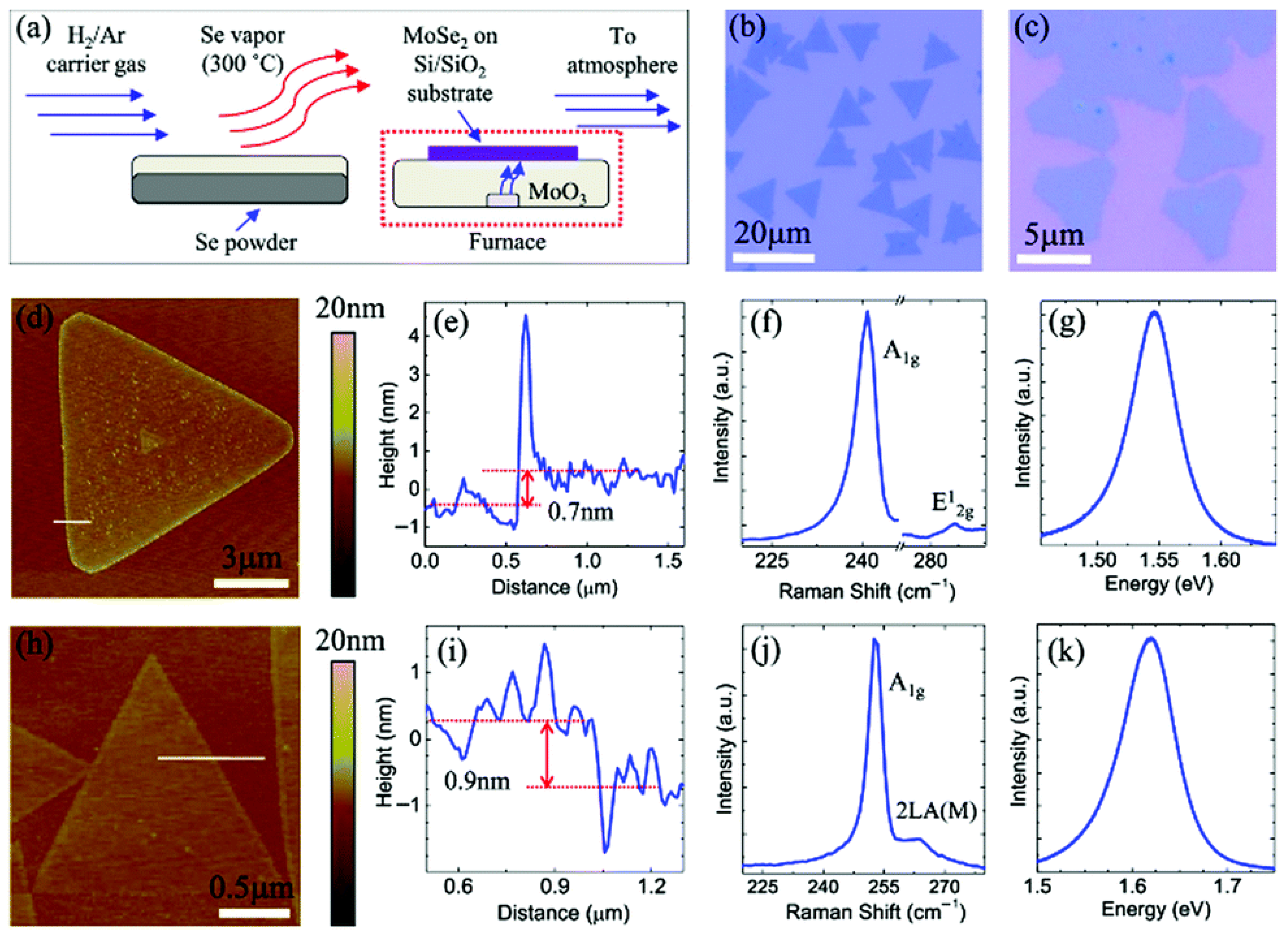
There are reports on the direct selenization of transition metal foils, which allows the production of homogeneous and highly crystalline few-layer TMSes [70]. One of the best-known examples is the growth of MoSe2 on Mo foil. Specifically, the material is synthesized by AP-CVD, where annealed Mo foil surfaces are subjected to direct selenization in selenium (Se) vapor at 550 °C for 60 min. Films obtained under these conditions reach sizes on the order of centimeters.
After synthesis, they can be easily transferred to various substrates by removing the Mo foil in a dilute ferric chloride (FeCl3) solution. The thickness of the transferred thin films on a SiO2/Si substrate (285 nm thick) ranges from 3.4 to 6 nm, as illustrated in detail in Figure 2a–k [71].
Figure 3 shows the central section of an UHVCVD reactor mounted in a 16-inch spherical stainless steel vacuum chamber. The heating station is mounted through the top flange, and the silicon wafer is fixed to a support beneath the heater with a gap that ensures uniform heating. The substrate temperature is monitored by a thermocouple located at a similar distance from the wafer.
On the lower flange of the chamber, quartz windows are connected to a microscope objective and an LED, mounted symmetrically on 1.75-inch diameter nipples. Additionally, a portable camera is attached to the vertically oriented retractable chamber. The colored lines in the diagram indicate the paths of the light rays. These optical components, together with the control and data acquisition systems, form a monitoring system that enables real-time monitoring of the sample surface condition, including the detection of micro- and macrodefects, as well as roughness [72].
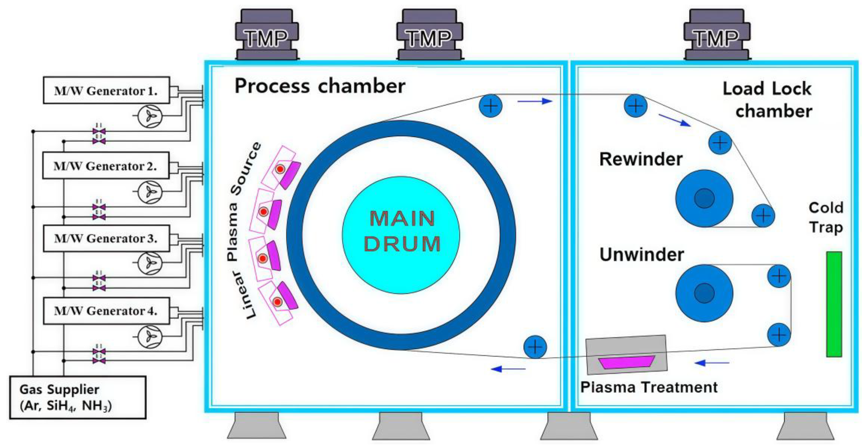
In MW-PECVD, plasma is excited by long-wavelength electromagnetic radiation, which ensures the formation of uniform and functionally stable coatings. For example, demonstrated the effectiveness of this approach for modifying polyethylene terephthalate (PET) by depositing a thin layer of hydrogenated amorphous silicon nitride (a-SiNx:H), which significantly improved the moisture barrier properties of the membrane. The experimental setup included a process and loading chambers; at a power of 1500 W and using SiH4 and NH3 gases, a uniform thin film was obtained (Figure 4). Furthermore, the method showed potential for the formation of oxidation-resistant coatings, as well as optically transparent superhydrophobic surfaces based on PDMS with a water contact angle of up to ~170° [73,74].
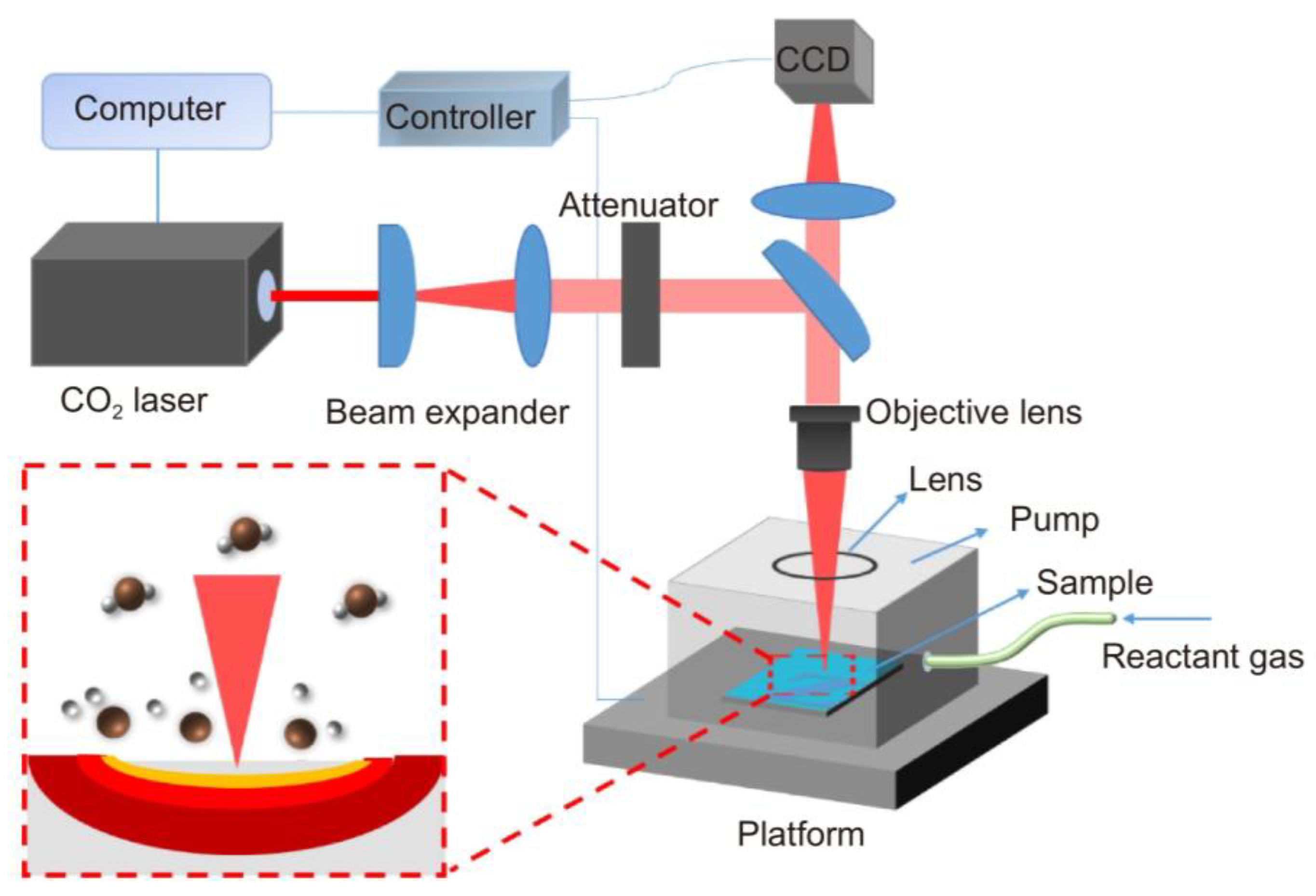
Figure 5 schematically illustrates a typical LCVD pyrolysis setup, comprising a precursor gas delivery system, a heater, a reaction vacuum chamber, a direct laser writing system, and a computerized control unit responsible for platform motion and processing trajectory.
In this configuration, continuous-wave (CW) lasers such as CO and Nd:YAG lasers are employed as the energy source for localized pyrolysis. The optical transmission system incorporates a beam expander, an attenuator, and a focusing lens (or half lens), which concentrate the laser beam onto the substrate surface, inducing localized heating and enabling selective material deposition.
The laser scanning trajectory is precisely controlled by a galvanometer mirror system or a 3D movable stage, allowing the fabrication of micro- and nanoscale structures with complex geometries. The substrate temperature is continuously monitored using pyrometers or thermocouples, while the precursor gas flow rate is regulated by mass flow controllers to ensure stable process conditions [76].
To improve the clarity of presentation, the refined figure includes labeled optical paths, highlighted laser–substrate interaction zones, and simplified flow diagrams to better illustrate the functional relationships among system components.
Thus, CVD and its many variations comprise a wide range of technologies enabling the production of coatings and functional layers with tailored structural, mechanical, and optical properties. From atmospheric AP-CVD to UHV-CVD, from PECVD to specialized CDCVD and iCVD methods, each modification meets specific technological requirements and finds application in electronics, membrane technologies, energy, and nanoengineering. Key parameters remain pressure, temperature, precursor composition, and energy source, determining the uniformity, selectivity, and functionality of the resulting coatings.

4. Morphological Evolution and Structural Features of CVD-Grown MoS2: The Influence of Growth Parameters, Substrate, and Holding Time

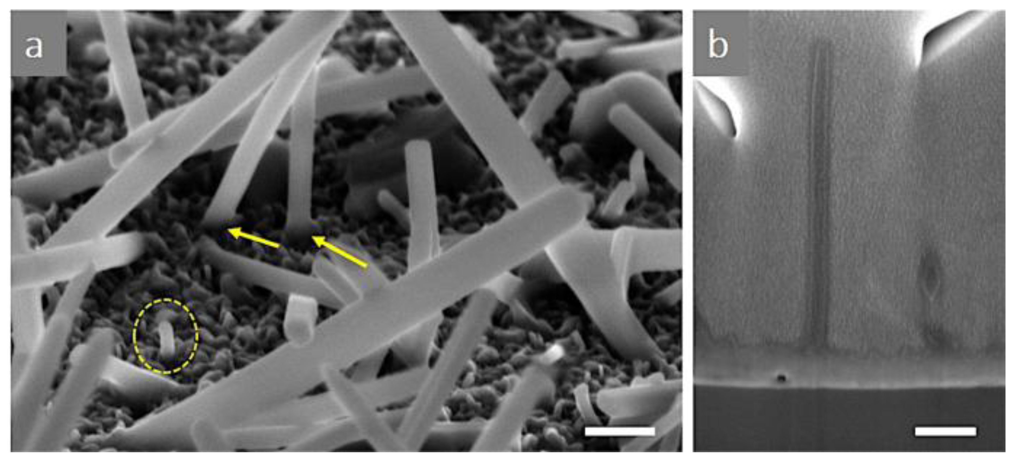
One promising approach to localized surface modification is the use of laser-induced deposition processes. In particular, LCVD enables the formation of coatings and micro- or nanostructures with high spatial selectivity by locally heating the substrate with laser radiation. Figure 6 shows a typical LCVD pyrolysis setup, including a precursor gas supply system, a heating element, a reaction vacuum chamber, an optical system for direct laser writing, and a control unit for platform movement and processing trajectory control. The nucleation and growth of MoS2 nanorods were investigated using SEM analysis. As shown in Figure 6a, a tilted-view SEM image reveals the initial formation of nanorod seeds on the MoS2 film surface, with arrows indicating the nucleation sites. A nanorod in its early stage of growth is highlighted by a yellow dotted line, illustrating the onset of vertical growth. Cross-sectional SEM imaging (Figure 6b) further confirms the vertical alignment of the nanorods and their uniform orientation. These observations demonstrate the controlled nucleation and subsequent growth of MoS2 nanorods, providing insight into the early-stage morphology and growth mechanism of the nanostructures [77].
Chemically synthesized MoS2 nanosheets demonstrate remarkable resilience in a typical lab environment (around 40% relative humidity), maintaining their integrity for roughly three years. Over time, however, a degradation process becomes apparent: nanorods, measuring several micrometers in length and mere nanometers in diameter, emerge from the original MoS2 seed structures. This growth is attributed to the chemical reaction between the MoS2 and oxygen and water vapor, leading to the formation of an amorphous molybdenum trioxide (MoO3) layer. Density functional theory calculations corroborate the critical involvement of water and oxygen in this transformation. The calculated adsorption energy of oxygen on the MoS2 surface (−1.09 eV) is substantially greater than that of water (−0.10 eV), suggesting that oxygen is preferentially adsorbed and initiates the oxidation of molybdenum atoms. Consequently, this research offers enhanced insight into the aging mechanisms of MoS2 when exposed to oxygen and moisture, a significant constraint on their real-world utility [78].
Figure 7a presents a scanning electron micrograph of the pristine MoS2 nanoparticles. The image reveals a dense, continuous arrangement of vertically aligned nanostructures, each 5–20 nm thick. These structures interlock to form a highly crystalline, interconnected network. Previous transmission electron microscopy investigations [78] have indicated that the exposed tips of these vertically oriented nanoparticles possess a sharp morphology, which is crucial for excellent field emission properties.
The development of the MoS2 structure closely reflects its morphological transformation. SEM analysis (Figure 8) reveals a variety of crystal shapes that depend strongly on the growth conditions, confirming the polycrystalline nature of the synthesized films [79]. These morphological variations are primarily governed by the local concentration balance of molybdenum and sulfur precursors within the confined-space CVD environment. In this process, sulfur is introduced from solid sulfur powder placed in a separate upstream heating zone. The controlled heating of this zone produces sulfur vapor, which is transported by the carrier gas into the reaction chamber, where it reacts with the MoO3 vapor to form MoS2.
The proximity between the MoO3 source and the substrate, as well as the relative temperatures of the sulfur and molybdenum zones, strongly influence the resulting Mo/S ratio during synthesis. At elevated temperatures (850–900 °C), variations in the sulfur vapor pressure alter the growth kinetics of the zigzag edges, which in turn determine the overall crystal morphology [80]. Due to the high chemical reactivity of these edge terminations, crystal growth proceeds preferentially along these directions rather than across the basal plane.
As a result, a diverse set of structural forms is observed, including triangular, three- and six-pointed star-like, and twinned crystals. The emergence of complex morphologies such as six-pointed stars is associated with the coalescence of misoriented grains exhibiting different lateral growth rates [81]. The occurrence of cyclic twins (Figure 8k) arises from the symmetrical intergrowth of adjacent crystal domains [82], while mirror twin boundaries form when MoS2 flakes rotate by 180° within the plane, producing characteristic inversion domains [83].
The CVD process utilized SiO2/Si, Si, and quartz glass as the base materials. Before deposition, these substrates underwent a thorough cleaning regimen involving ultrasonic treatment in deionized water, a detergent solution, alcohol, and sulfur powder. The source materials for the deposition were WO3 and MoO3 powders (sourced from Aladdin Industrial Co., Ltd., Pico Rivera, CA, USA). In a tube furnace (model BTF-400C from BEQ Co., Ltd., Newark, DE, USA), Si (weighing 0.3 g) was positioned above a mixture of MoO3/WO3 (0.1 g) within distinct heating zones (as illustrated in Figure 9). The substrates were then placed face-down onto a boat containing the MoO3/WO3 mixture.
Figure 8. SEM images of MoS2 crystals grown on SiO2 substrate at a growth temperature of 780 °C with a MoO3/S ratio of 1:20 and 25 mg NaCl. (ad) SEM images of MoS2 with low magnification. High-magnification SEM images of various shapes of CVD-grown MoS2: (e) three-point star, (f) four-point star, (g) tilt boundary, (h) mirror boundary, (i,j) six-point star, (k) seven-point star, and (l) mirror twins [84].
Crystals 15 01037 g008
The synthesis of MoS2 was carried out using a two-zone CVD system, in which the sulfur and molybdenum oxide (MoO3) precursors were placed in separate temperature zones to ensure controlled vapor transport and reaction. During the process, the sulfur source was heated to 200 °C to generate sulfur vapor, while the MoO3 and Si substrate zone was maintained at 650 °C for 45 min. After this stage, the system was held at these temperatures for an additional 5 min before being allowed to cool naturally (Figure 9b).
For the synthesis of WS2, an analogous procedure was followed, with sulfur and tungsten oxide (WO3) serving as the precursor pair. The sulfur zone was again heated to 200 °C, while the WO3 and substrate zone was maintained at 1000 °C for 90 min. Throughout both processes, a constant nitrogen (N2) flow of 40 sccm was used as the carrier gas to transport sulfur vapor into the reaction zone and facilitate the formation of the dichalcogenide films. This methodology ensured stable sulfur delivery, uniform reaction conditions, and reproducible film growth, as reported in [85].
Figure 9. SEM image of MoS2 grown on (a) NFT SiO2/Si; (b) PTCDA SiO2/Si; (c) O2 plasma-cleaned SiO2/Si; (d) NFT Si; (e) PTCDA Si; (f) O2 plasma-cleaned Si [85].
Crystals 15 01037 g009
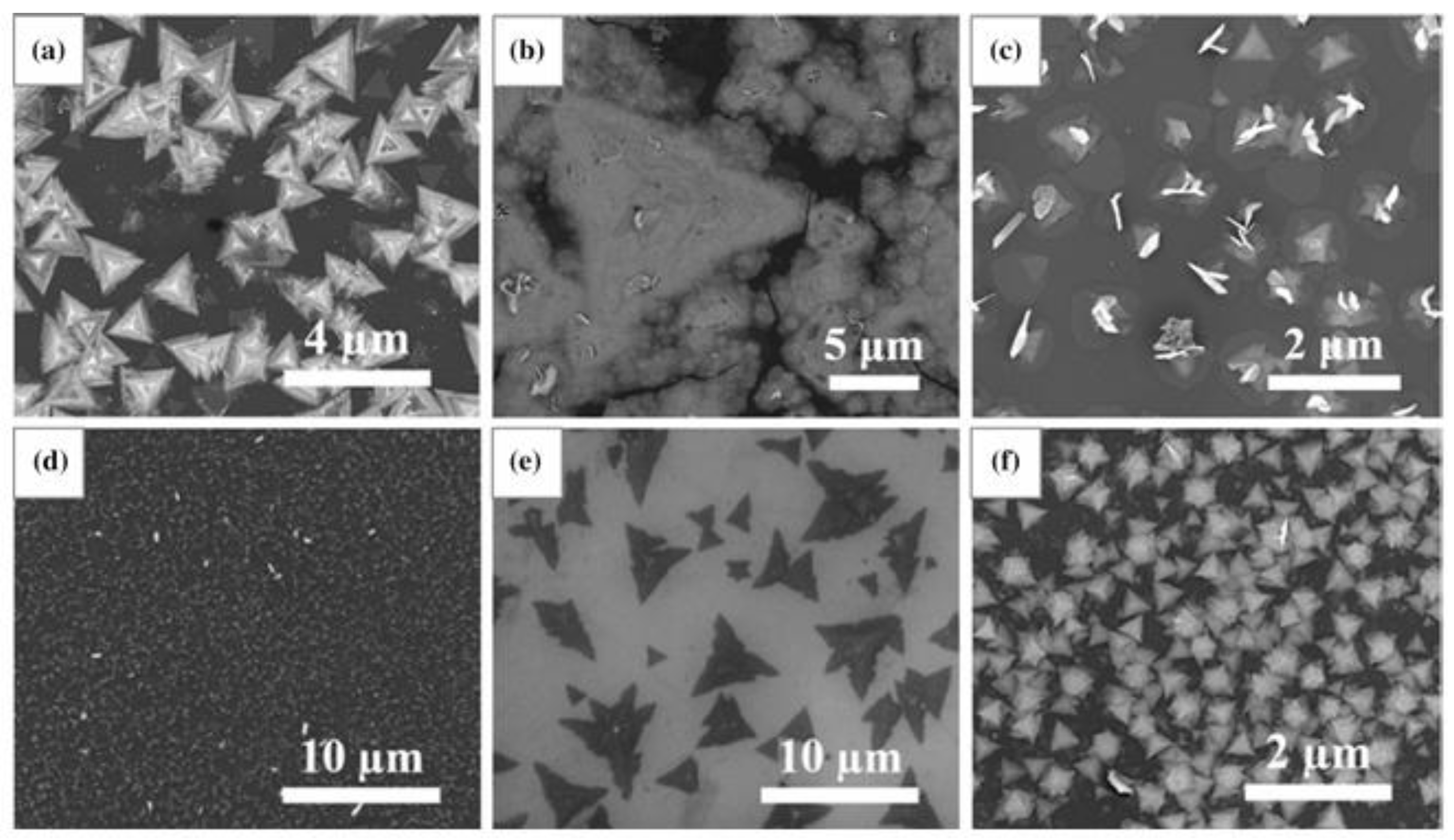
Figure 10 shows SEM images of samples synthesized under different growth conditions, demonstrating a close correlation between the MoS2 morphology and the process parameters. At low inert gas flow rates, high TS (substrate temperature), and low TG (growth temperature) values, dendritic growth is observed due to the increased sulfur concentration, which leads to the formation of irregularly shaped crystals with significant lateral dimensions (Figure 10a). Low TG promotes the activation of multiple growth centers. Decreasing the sulfur evaporation temperature reduces its partial pressure, causing a transition in geometry from dendritic to concave triangular (Figure 10b). With a further increase in temperature, growth leads to the formation of triangular and truncated triangular crystals. In general, increasing the temperature and/or increasing the Mo/S ratio contributes to greater compactness of the structure and a decrease in its concavity [86].
An analysis of literature data and SEM images revealed that the morphology of MoS2 synthesized by CVD is closely dependent on process parameters, substrate type, and long-term storage conditions. Vertically oriented nanoparticles with a high degree of crystallinity can transform into nanorods over time, demonstrating structural evolution under environmental influences.
A comparison of various studies indicates that the Mo/S ratio, evaporation temperature, and growth temperature play a key role in the formation of MoS2 crystals of various shapes—from simple triangles to complex multi-arm stars and twins. Increasing the growth temperature and optimizing the sulfur partial pressure promote the formation of more compact crystals with an ordered morphology. Furthermore, the use of different substrates (SiO2/Si, Si, quartz glass) directly influences crystal nucleation and orientation, determining grain boundaries and the defect structure of the material. Thus, controlling growth conditions during CVD allows for targeted regulation of the morphology and structural characteristics of MoS2, opening up prospects for its application in electronics, optoelectronics, and nanoenergy. Further research should focus on precisely correlating growth parameters, morphology, and the material’s functional properties to develop reproducible methods for producing high-quality single-crystal MoS2 films.

5. XPS Investigation of Defect States, Oxidation, and Interfacial Chemistry in MoS2 Heterostructure
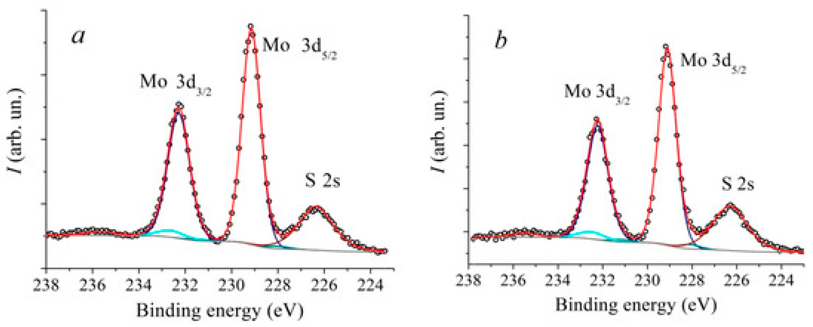
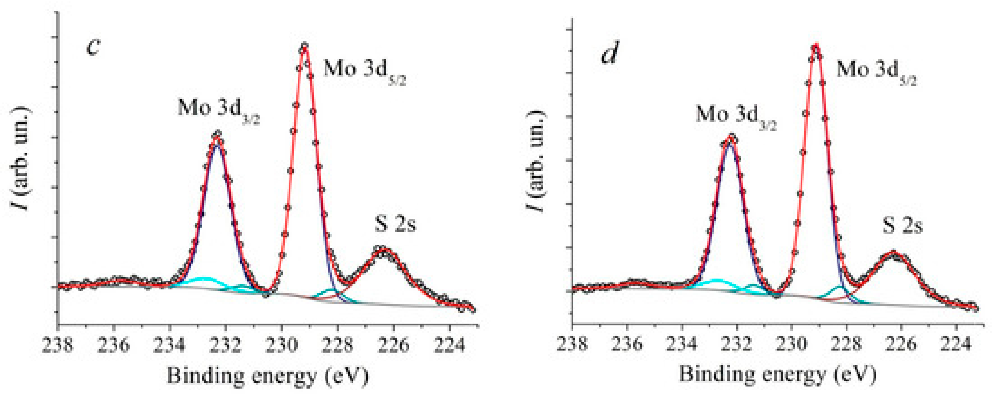
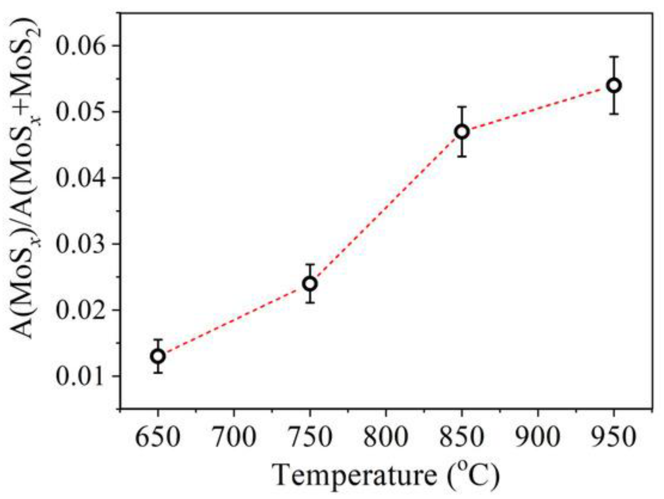
X-ray photoelectron spectroscopy (XPS) was employed to examine the chemical states of molybdenum and sulfur in MoS2 films synthesized at different temperatures. Figure 11 and Figure 12 display the XPS spectra for the Mo3d and S2p core levels, respectively. The Mo3d spectra were resolved into three distinct doublets. The first, with a Mo3d5/2 binding energy (BE) of 229.1 eV and a spin–orbit splitting of 3.15 eV, corresponds to Mo4+ in 2H-MoS2. The second doublet, at 232.5 eV, indicates Mo6+ in MoO3, while the third, at 228.3 eV, is linked to Mo in substoichiometric MoSx [87,88]. Notably, Mo6+ concentration remained consistently around 5 at.%, whereas the MoSx fraction increased with deposition temperature from ~1.3 at.% to ~5.4 at.% [89].
These results highlight temperature’s critical role in forming substoichiometric MoSx phases, which impacts structural and electronic properties. Understanding these correlations is vital for optimizing MoS2 growth and its performance in applications like catalysis, electronics, and energy storage. This work systematically explores the effect of deposition temperature on the structural, chemical, and electronic characteristics of MoS2 thin films.
Figure 13 illustrates the temperature dependence of the MoSx concentration estimated from XPS data. According to [90], the BE of 228.3 eV for MoSx corresponds to a [S]/[Mo] ratio of ~1.3. In stoichiometric MoS2, each Mo atom is bonded to six S atoms, while in MoSx this ratio implies that each Mo atom lacks, on average, two S neighbors. To avoid triple counting of missing S atoms, the concentration of sulfur vacancies (Vs) was calculated as [89]:
V s 2 M o x + 3 M o x + + M o 4 + × 100 %
where Mox+ represents the MoSx component intensity and Mo4+ the MoS2 component intensity. The results indicate that Vs increases with deposition temperature, rising from ~0.9 at.% at 650 °C to ~3.6 at.% at 950 °C.
The [S]/[Mo] ratio, when calculated directly, remains remarkably stable at 2.0 ± 0.1 for every sample. Nevertheless, this direct calculation is unable to reveal subtle compositional variations close to the XPS sensitivity limit. Additionally, the S2p spectra undergo minor alterations with increasing temperature, including a small shift (approximately 0.1 eV) towards reduced binding energy [89].
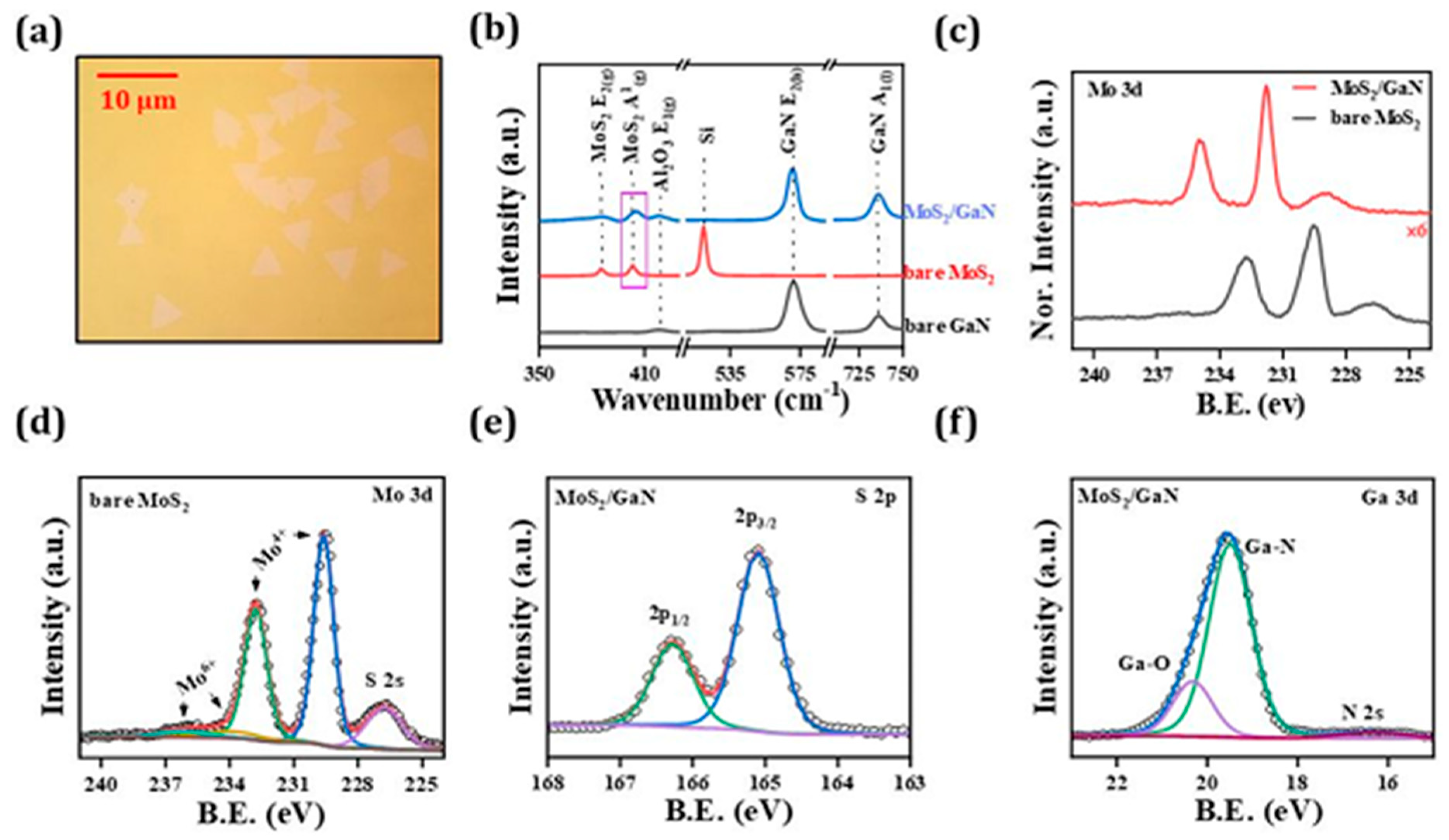
Figure 14 presents a detailed characterization of MoS2 grown on untreated GaN substrates. Panel (a) shows an optical image of the MoS2 flakes, revealing lateral sizes of approximately 5 µm. The Raman spectra in panel (b) compare MoS2/GaN with pure MoS2 and GaN, showing characteristic GaN peaks at E2(high) = 570.1 cm−1, A1(low) = 736.5 cm−1, and Al2O3 E1(g) = 418.2 cm−1, alongside the MoS2 E2(g) (~385.8 cm−1) and A1(g) (~403.2 cm−1) modes. For the MoS2/GaN heterostructure, the A1(g) peak shifts to 405.5 cm−1, indicating a blue shift upon interaction with the substrate. The peak separation Δk between E2(g) and A1(g) increases from 17.4 cm−1 in pure MoS2 to 19.7 cm−1 in the heterostructure, while an additional Si-related peak is observed at 520.7 cm−1.
Panels (c–e) show XPS analysis of the core levels of Mo (3d), S (2p), and Ga (3d). Charge correction was applied using C 1s at 284.6 eV. The Mo (3d) spectrum displays peaks at 229.6 eV (Mo 3d5/2) and 232.8 eV (Mo 3d3/2), confirming Mo-S bonding in the Mo4+ state, with minor features at 233.8 eV and 236.3 eV corresponding to Mo6+ states (Mo-O). The S (2s) peak at 226.8 eV further supports Mo-S bonding. Deconvolution of the S (2p) spectrum reveals a spin–orbit doublet at 165.1 and 166.3 eV (Δ = 1.2 eV), consistent with the formation of MoS2. Using these data, the sulfur stoichiometry and vacancy concentration were estimated [90].
These results collectively demonstrate that the MoS2/GaN heterostructure maintains the intrinsic chemical composition of MoS2 while exhibiting substrate-induced modifications in vibrational properties, highlighting the role of substrate interactions in tuning the structural and electronic characteristics of the films.
S ( at . % ) Mo ( at . % ) = I S ( 2 s ) σ S ( 2 s ) I Mo 3 d 5 2 σ Mo 3 d 5 2
Atomic percentages of sulfur and molybdenum are indicated by S (atomic %) and Mo (atomic %), respectively. The integrated peak intensities for S (2s) and Mo (3d5/2) are designated as IS (2s) and IMo 3d(5/2). The parameters σS(2s) and σMo3d(5/2) are obtained from well-regarded scholarly publications [91]. Analysis of the Ga (3d) level in the heterostructure, as shown in Figure 14e, demonstrates three identifiable components after peak deconvolution. The most significant component is associated with Ga-N bonds, while the other two are attributed to Ga-O bonds and the N (2s) state. This interpretation is in agreement with existing literature [92].
Figure 14. (a) Optical Image of MoS2 on untreated GaN (b) Raman spectra of bare GaN, bare MoS2 and the heterostructure. (c) XPS Mo-3d Spectra for MoS2/GaN compared with bare MoS2. (d) XPS core level spectra of bare MoS2, (e) Mo-3d and S 2p, and (f) Ga-3d for the heterostructure [92].
Crystals 15 01037 g014
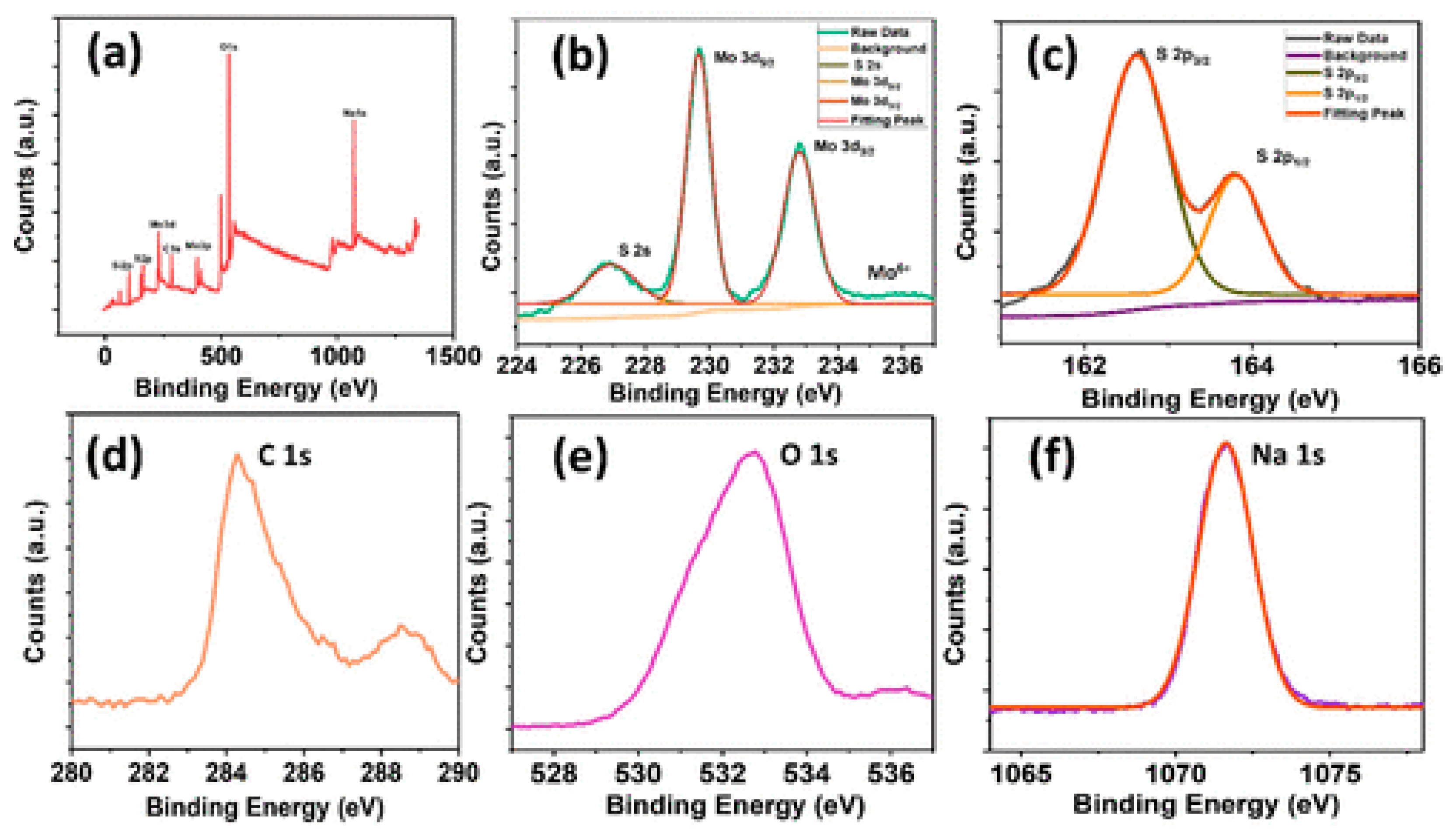
To thoroughly investigate the atomic makeup, chemical characteristics, and the influence of NaCl during the formation of MoS2, XPS was employed on MoS2 crystals produced at 780 °C (Figure 15).
Figure 15a presents the overall spectrum of the MoS2 sample. Detailed analysis of the Mo 3d region (Figure 15b) revealed binding energy (BE) peaks at 229.68 and 232.80 eV. These correspond to the 3d5/2 and 3d3/2 orbitals of Mo in a +4 oxidation state (Mo4+), which is the expected state for molybdenum within the MoS2 crystal structure [93]. A minor peak observed at 235.98 eV is likely attributable to molybdenum oxides, possibly MoO3. This could stem from unreacted MoO3 starting materials, a common occurrence in MoS2 synthesized via CVD, and would manifest as peaks for Mo in a +6 oxidation state (Mo6+) [94,95].
A Mo 3d5/2 peak at 226.99 eV suggests some degree of sulfur oxidation. The S 2p spectra (Figure 15c) displayed spin–orbit split peaks at 162.62 and 163.80 eV, representing the 2p3/2 and 2p1/2 states, respectively, with an energy difference of 1.18 eV. For calibration purposes, the C 1s peak was found at 284.28 eV (Figure 15d), and the O 1s peak was centered at 532.78 eV, likely originating from an oxide layer on the silicon substrate (Figure 15e). Furthermore, the Na 1s spectrum showed a peak at 1071.69 eV (Figure 15f), confirming the presence of sodium. This indicates that sodium from the NaCl precursor may persist under the MoS2 crystals as intermediate growth compounds, such as Na2MoxOx [96] and Na2SO4 [97].
Figure 15. XPS analysis of MoS2 grown at 780 °C: (a) XPS survey. (b) Peaks for Mo 3d orbitals 3d5/2 and 3d3/2 at 229.68 and 232.80 eV, respectively. Sulfur oxidation peak at 226.99 eV. A peak of low intensity observed at 235.98 eV representing MoO3. (c) Orbitals of S 2p, 2p3/2 and 2p1/2, observed at 162.62 and 163.80 eV, respectively. (d) Carbon calibration peak at 284.28 eV. (e) O 1s peak at 532.78 eV representing the oxide layer of the Si substrate. (f) Na 1s peak observed at 1071.69 eV representing Na2MoxOx or Na2SO4 [96,97].
Crystals 15 01037 g015
XPS studies showed that the chemical state and stoichiometry of MoS2 depend significantly on both the synthesis temperature and storage conditions. Mo 3d spectra confirm the presence of three components: Mo4+ in the 2H-MoS2 structure, 6+ as MoO3 impurities, and a nonstoichiometric MoSx phase. With increasing synthesis temperature, the MoSx concentration increases, indicating an increase in the number of sulfur vacancies (Vs) in the material. Additionally, a shift and change in the shape of the S 2p peaks is observed, indicating defects and a change in the chemical environment of sulfur [98,99,100].
Long-term aging of the samples in air and moisture leads to increased oxidation of MoS2, manifested by an increase in the intensity of the MoO3 peaks and the formation of S-O bonds. These results are consistent with Raman spectroscopy data, which reveal signatures of MoO3. For MoS2/GaN heterostructures, XPS and Raman analysis reveal strong chemical interactions at the interface, including shifts in the positions of characteristic peaks, indicating the influence of sulfur defects and interfacial bonds [101,102,103].
Thus, XPS analysis confirmed the key role of growth temperature and storage conditions in the formation of sulfur vacancies, oxidized phases, and interfacial interactions. These factors directly affect the electronic and optical properties of MoS2 and should be considered when developing functional heterostructures and devices.

6. Investigation of DC Conductivity, Gas Sensing, and Electrochemical Behavior of MoS2 Nanocomposites
A wide variety of studies have investigated the application potential of MoS2-based materials in fields such as gas sensing, electrochemical energy storage, and battery technology, demonstrating the material’s multifunctionality and adaptability. However, no unified criterion was applied in selecting these references; instead, this section presents representative examples illustrating the broad range of MoS2 functionalities reported in the literature.
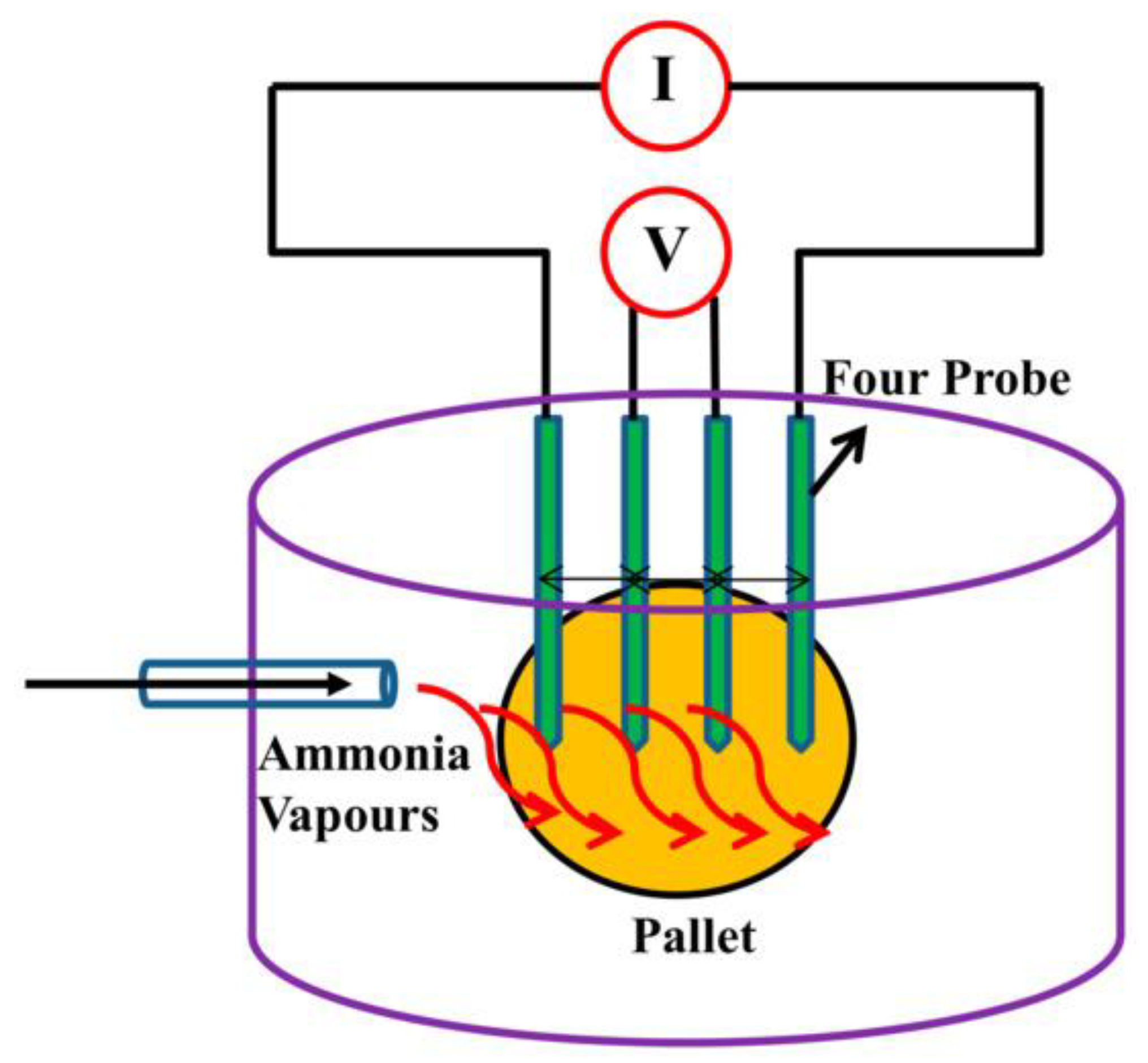
To explore the electrical and sensing performance of MoS2 and its polymer composites, several studies have employed four-probe conductivity measurements under controlled environments. For instance, the DC conductivity and ammonia sensing behavior of MoS2, polypyrrole (PPy), and PPy/MoS2 nanocomposites were examined using a four-probe setup coupled with a PID-controlled furnace [104]. As shown schematically in Figure 16, this configuration enabled precise temperature control and reliable data acquisition, establishing a foundation for understanding the interrelation between material structure and sensing response.
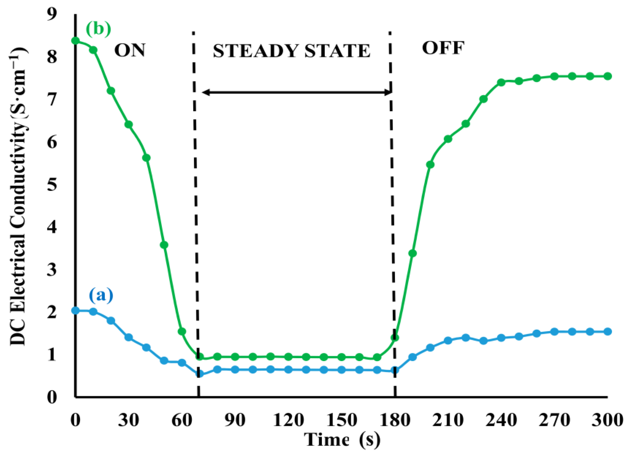
Figure 17 illustrates the standard four-probe method employed to ascertain the initial direct current (DC) conductivity of MoS2, PPy, and PPy/MoS2 nanocomposites. Room temperature measurements revealed conductivities of 2.2 × 10⁻⁶ S·cm−1 for MoS2, 2.03 S·cm−1 for PPy, and 8.33 S·cm−1 for PPy/MoS2. The incorporation of MoS2 into PPy resulted in a remarkable surge in the nanocomposite’s conductivity. This significant enhancement is attributed to the interaction between the lone pair electrons of nitrogen in polypyrrole and the molybdenum centers of MoS2, which is proposed to generate additional holes in PPy, thereby elevating its electrical conductivity [104].
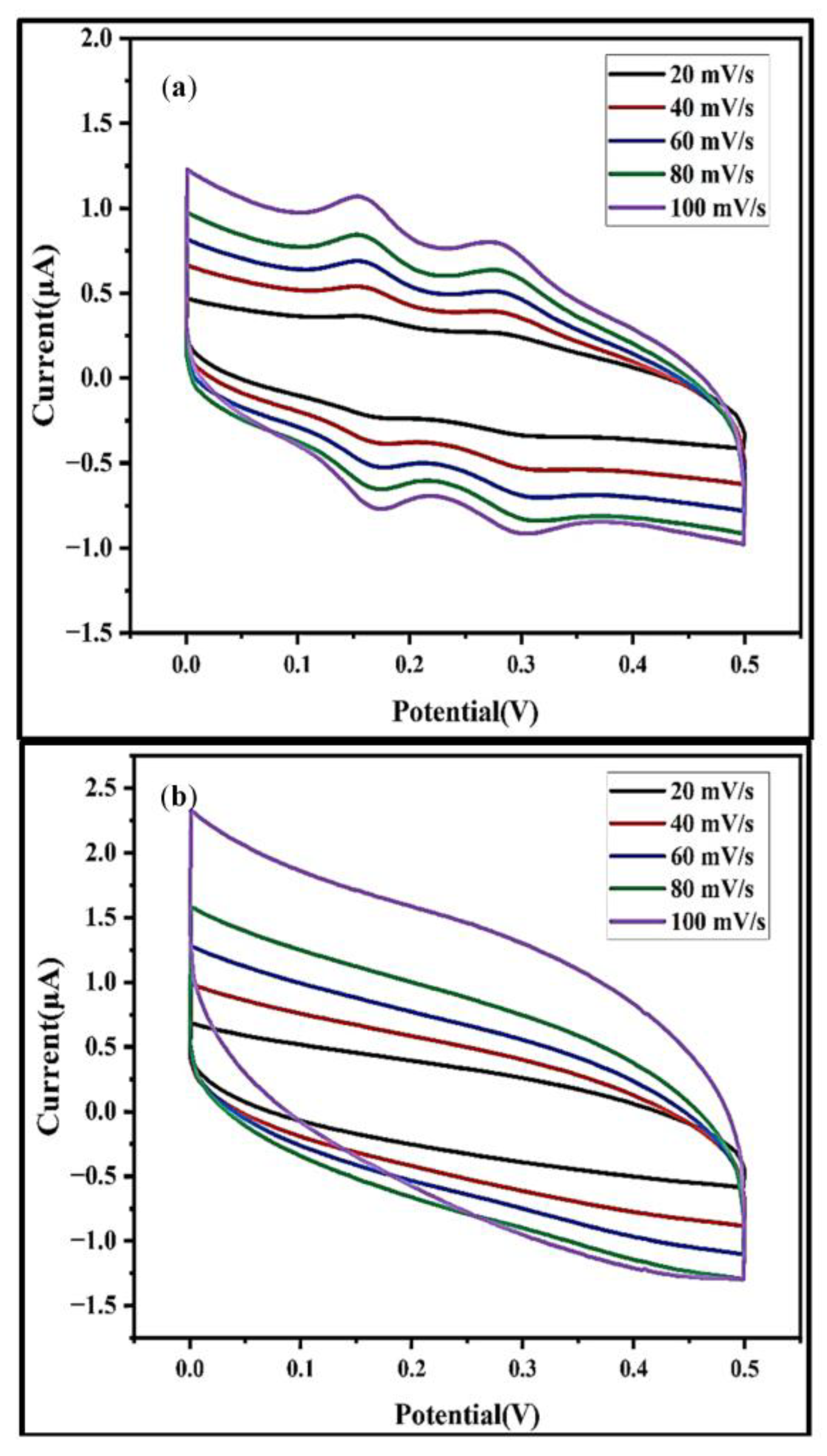
The electrochemical performance of MoS2/BC3 nanocomposite, pristine BC, and pure MoS2 nanosheet electrodes is depicted in Figure 18 through cyclic voltammetry curves. These were recorded in 1 M H2SO4 electrolyte within the 0–0.5 V potential window at scan rates from 20 to 100 mV·s−1. For improved clarity and comparison, the figure has been refined with consistent colors, normalized current scales, and clear scan rate labels [105,106,107].
Quasi-rectangular CV profiles were observed for the MoS2/BC3 NC and pristine BC electrodes, signifying the presence of both electric double-layer capacitance and pseudocapacitance. The MoS2 NS electrode, however, displayed distinct faradaic redox peaks, characteristic of purely pseudocapacitive behavior [108,109,110].
The integration of the porous BC3 framework with MoS2 nanosheets in the composite resulted in a substantially larger CV area and a higher specific capacitance (34 F·g−1 at 20 mV·s−1), confirming enhanced charge storage due to synergy. The improved Figure 17 clearly highlights these electrochemical differences and the superior capacitive capabilities of the MoS2/BC3 nanocomposite [111].
Figure 18. CV profiles of (a) pristine MoS2 NSs, (b) pristine BC [111].
Crystals 15 01037 g018
Figure 18a,b presents the cyclic voltammetry curves for electrodes incorporating MoS2/BC3 nanocomposites. For comparison, the CV profiles of unmodified BC and MoS2 nanosheets are also shown. These measurements were conducted within a potential range of 0–0.5 V, employing scan rates from 20 to 100 mV·s−1 in a 1 M H2SO4 electrolyte. Electrodes featuring the MoS2/BC3 NC and those based on BC alone demonstrated CV shapes that were nearly rectangular. This suggests that their capacitive behavior arises from a combination of electric double-layer capacitance and pseudocapacitive processes. In contrast, electrodes made with MoS2 NS exhibited distinct faradaic redox peaks, indicative of pseudocapacitance.
The synergistic integration of the highly porous BC framework with the layered MoS2 NS within the MoS2/BC3 NC led to a larger CV area, which in turn translated to a higher specific capacitance. At a scan rate of 20 mV·s−1, the composite material achieved a specific capacitance of 34 F·g−1, substantially exceeding the capacitance values of the individual MoS2 and BC components. At slower scan rates, the capacitance further improved, attributed to more extensive ion penetration into the porous structure.
These findings underscore a cooperative interaction between MoS2 and BC, which enhances the specific surface area, electrical conductivity, and overall capacitive performance. This highlights the potential of MoS2/BC3 NC as a cutting-edge material for hybrid supercapacitor applications [112].
Given the growing demand and escalating prices of lithium-ion batteries (LIBs), sodium-ion batteries (SIBs) have attracted increasing attention as a cost-effective and sustainable alternative for large-scale energy storage. To achieve the commercial viability of SIBs, further progress in electrode materials, electrolytes, and current collector design remains essential. In particular, the development of advanced electrode fabrication techniques and strategies aimed at enhancing specific capacity and cycling stability can accelerate their integration into practical systems.
Among various electrode candidates, MoS2-based materials have demonstrated promising electrochemical properties due to their layered structure, high surface area, and efficient ion intercalation capability. Numerous studies have reported on MoS2 composites and heterostructures tailored for improved performance in SIBs. Table 3 provides a comparative summary of recent research efforts on MoS2-based battery systems, highlighting the diversity of synthesis approaches, structural modifications, and electrochemical characteristics investigated across different studies [113].
Studies of the electrical conductivity and electrochemical properties of composites based on MoS2 and carbon-containing materials (PPy, BC, PANI, graphene, etc.), as well as thin films of gold nanorods and nanoparticles, demonstrated a significant improvement in the functional properties of the materials when forming hetero- and nanostructures [126,127,128]. The introduction of MoS2 into the polymer matrix led to a sharp increase in electrical conductivity due to the interaction of nitrogen-containing centers with molybdenum, while multilayer structures of gold nanorods provided a dramatic reduction in sheet resistance and an increase in conductivity [129,130].
Electrochemical studies confirmed the synergistic effect between MoS2 and carbon materials, manifested in improved capacitive behavior and an increase in specific capacitance, making these composites promising for the development of hybrid supercapacitor electrodes. Furthermore, microwave absorbers based on MoS2-PANI demonstrated high absorption of electromagnetic radiation due to their increased specific surface area and improved electrical conductivity. A comparative analysis of lithium- and sodium-based batteries using MoS2/carbon composite materials revealed that optimization of morphology (nanocables, nanobundles, nanocups, nanotubes, etc.) and synthesis methods (hydrothermal, solvothermal, carbonization, etc.) provides a significant increase in specific capacity-up to 1275 mA h g−1. This confirms that modified MoS2 structures play a key role in the creation of new generations of energy storage devices and functional materials.
Thus, the development of MoS2-based composites opens up broad prospects for sensors, supercapacitors, microwave absorbers, and next-generation batteries.

7. Challenges and Future Directions

Despite considerable advancements in creating and utilizing MoS2-based nanocomposites, several fundamental and practical hurdles persist. Overcoming these limitations is vital to fully unlock the capabilities of MoS2 thin films and coatings for next-generation systems in energy, electronics, and protection.
  • Managing Structural Imperfections and Layer Consistency.
Achieving consistent, defect-free MoS2 layers is a primary challenge for large-scale production. Discrepancies in sulfur content, grain boundaries, and stacking faults significantly impact MoS2’s electronic and catalytic effectiveness. Future investigations should prioritize real-time monitoring during CVD growth to precisely control layer thickness, nucleation density, and defect formation.
  • Scaling Up and Ensuring Consistency in Deposition Techniques.
While CVD and its variations yield high-quality films, achieving scalability without sacrificing crystal perfection remains difficult. Hybrid deposition systems, such as plasma-assisted or low-temperature CVD, could bridge the gap between laboratory-scale production and industrial application. Furthermore, understanding the thermodynamics of precursor breakdown and gas flow dynamics is crucial for improving process reliability.
  • Optimizing Interfaces and Adhesion.
Robust interfacial bonding between MoS2 and various substrates (metals, ceramics, or polymers) is essential for mechanical resilience and long-term performance. Poor adhesion frequently leads to separation or cracking under thermal or mechanical stress. Future studies should explore strategies for modifying interfaces, including gradient coatings, intermediate adhesion layers, or surface functionalization methods.
  • Ensuring Durability in Various Environments and Operating Conditions.
MoS2-based coatings can degrade through oxidation, phase changes, or breakdown when exposed to high temperatures, humidity, and corrosive chemical environments. Developing passivation techniques, protective encapsulation layers, or compositional modifications (e.g., MoS2/graphene or MoS2/h-BN hybrids) could significantly enhance their longevity and dependability in demanding conditions.
  • Integrating Analysis and Data-Driven Refinement.
The intricate relationship between MoS2 synthesis, its structure, and its properties necessitates sophisticated characterization and modeling approaches. Combining in situ spectroscopy, machine learning algorithms, and high-throughput simulations will expedite the discovery of optimized synthesis methods and performance predictions for specific applications.
  • Tailoring Designs for Specific Applications and Identifying Niche Uses.
While MoS2 has been extensively researched for catalysis and energy storage, its potential in protective coatings, flexible electronics, tribology, and thermal management remains largely unexplored. Future research should focus on identifying these specialized areas where MoS2 thin films can offer unique advantages, such as low friction or radiation resistance.

8. Conclusions

This review evaluated the key factors governing the synthesis and properties of MoS2, with an emphasis on CVD while also considering the broader context of alternative fabrication methods. Although CVD remains the most versatile approach for producing wafer-scale and high-quality MoS2 films, the analysis shows that material characteristics cannot be fully understood without comparing CVD results to exfoliation, hydrothermal growth, sulfurization of Mo/MoO3 layers, and plasma-assisted techniques. These methods differ significantly in defect density, grain size, surface uniformity, and scalability, and their omission may lead to an incomplete understanding of structure-property relationships.
Raman, XPS, and PL characterizations consistently confirmed the formation of layered MoS2, but the comparison of different synthesis strategies revealed that the stability of vibrational modes, oxidation tendency, and excitonic responses strongly depend on growth route and post-growth environment. In particular, sulfur deficiency and surface oxidation remain common challenges across all synthesis techniques, not only CVD-derived films. This underscores the need for improved passivation strategies and controlled atmosphere processing.
Importantly, the review highlights that the performance of MoS2 is shaped by three interconnected factors:
(1)
Synthesis method and associated growth conditions;
(2)
Defect chemistry and stoichiometric deviations;
(3)
Environmental stability during storage and operation.
A critical comparison of recent studies shows that optimizing only one of these factors is insufficient; reliable device functionality requires an integrated approach that accounts for all three.
Looking ahead, future progress should focus on unifying experimental and theoretical efforts. This includes using in situ diagnostics, kinetic modeling, and surface engineering to control defect formation mechanisms and interfacial processes with higher precision. A more systematic comparison of CVD with alternative growth techniques is also essential for establishing clear guidelines for selecting synthesis routes based on target applications.
Such a framework will support the rational design of MoS2-based materials for electronics, optoelectronics, catalysis, and protective coatings, enabling a more consistent transition from laboratory demonstrations to practical technologies.

Author Contributions

Conceptualization, S.R. and G.O.; methodology, D.B.; software, B.K.; validation, K.K., A.T. and S.R.; formal analysis, B.K.; investigation, D.B.; resources, G.O.; data curation, K.K.; writing—original draft preparation, S.R.; writing—review and editing, N.M.; visualization, G.O.; supervision, N.M.; project administration, A.T.; funding acquisition, G.O. All authors have read and agreed to the published version of the manuscript.

Funding

This research is funded by the Committee of Science of the Ministry of Science and Higher Education of the Republic of Kazakhstan (Grant No. BR24992854).

Data Availability Statement

No new data were created or analyzed in this study.

Conflicts of Interest

The authors declare no conflict of interest.

References

  1. Chong, K.; Zou, Y.; Wu, D.; Tang, Y.; Zhang, Y. Pulsed Laser Re-Melting Supersonic Plasma Sprayed Cr3C2-NiCr Coatings for Regulating Microstructure, Hardness, and Corrosion Properties. Surf. Coat. Technol. 2021, 418, 127258. [Google Scholar] [CrossRef]
  2. Ping, X.L.; Fu, H.G.; Sun, S.T.; Lin, J.; Guo, X.Y.; Lei, Y.P. Microstructure and Performance of Nb-Bearing Ni60A-Cr3C2 Coatings Manufactured by Laser Cladding. Surf. Eng. 2020, 36, 1294–1306. [Google Scholar] [CrossRef]
  3. Sadeghimeresht, E.; Markocsan, N.; Nylen, P. Microstructural Characteristics and Corrosion Behavior of HVAF-and HVOF-Sprayed Fe-Based Coatings. Surf. Coat. Technol. 2017, 318, 365–373. [Google Scholar] [CrossRef]
  4. Zhu, L.; Wang, S.; Pan, H.; Yuan, C.; Chen, X. Research on Remanufacturing Strategy for 45 Steel Gear Using H13 Steel Powder Based on Laser Cladding Technology. J. Manuf. Process. 2020, 49, 344–354. [Google Scholar] [CrossRef]
  5. Mehta, J.; Grewal, J.S.; Gupta, P. Analysis of D-gun Sprayed Coating on Medium Carbon Steel. Mater. Today Proc. 2020, 21, 1403–1406. [Google Scholar] [CrossRef]
  6. Romanchenko, O.; Porkuian, O.; Kharlamov, Y.; Sokolov, V.; Krol, O. Research of Features of Oxide Coatings Deposition by D-gun Spraying. In Innovations in Mechanical Engineering II, Proceedings of the International Conference Innovation in Engineering, Minho, Portugal, 28–30 June 2022; Springer International Publishing: Cham, Switzerland, 2022; pp. 305–316. [Google Scholar] [CrossRef]
  7. Li, X.; Zhai, H.; Li, W.; Cui, S.; Ning, W.; Qiu, X. Dry Sliding Wear Behaviors of Fe-Based Amorphous Metallic Coating Synthesized by D-gun Spray. J. Non-Cryst. Solids 2020, 537, 120018. [Google Scholar] [CrossRef]
  8. Hallad, S.A.; Banapurmath, N.R.; Hunashyal, A.M.; Shettar, A.S. Study of the Effect of Nanocomposite Thin Film Coating on Cutting Tool Tip for Tribological Applications. Mater. Today Proc. 2020, 27, 37–39. [Google Scholar] [CrossRef]
  9. Sabzi, M.; Mousavi Anijdan, S.H.; Asadian, M. The Effect of Substrate Temperature on Microstructural Evolution and Hardenability of Tungsten Carbide Coating in Hot Filament Chemical Vapor Deposition. Int. J. Appl. Ceram. Technol. 2018, 15, 1350–1357. [Google Scholar] [CrossRef]
  10. Perez-Mariano, J.; Lau, K.H.; Alvarez, E.; Malhotra, R. Coatings for Corrosion Protection of Porous Substrates in Gasifier Components. Surf. Coat. Technol. 2008, 202, 2794–2800. [Google Scholar] [CrossRef]
  11. Delfini, A.; Vricella, A.; Bueno Morles, R.; Pastore, R.; Micheli, D.; Gugliermetti, F.; Marchetti, M. CVD Nano-Coating of Carbon Composites for Space Materials Atomic Oxygen Shielding. Procedia Struct. Integr. 2017, 3, 208–216. [Google Scholar] [CrossRef]
  12. Li, Z.; Wang, Y.; Xiong, X.; Li, X.; Chen, Z.; Sun, W. Microstructure and Growth Behavior of HfC Ceramic Coating Synthesized by Low Pressure Chemical Vapor Deposition. J. Alloys Compd. 2017, 705, 79–88. [Google Scholar] [CrossRef]
  13. Mousavi Anijdan, S.H.; Sabzi, M.; Asadian, M.; Jafarian, H.R. Effect of Sub-Layer Temperature during HFCVD Process on Morphology and Corrosion Behavior of Tungsten Carbide Coating. Int. J. Appl. Ceram. Technol. 2019, 16, 243–253. [Google Scholar] [CrossRef]
  14. Strauss, H.W.; Chromik, R.R.; Hassani, S.; Klemberg-Sapieha, J.E. In Situ Tribology of Nanocomposite Ti-Si-C-H Coatings Prepared by PE-CVD. Wear 2011, 272, 133–148. [Google Scholar] [CrossRef]
  15. Xu, M.; Ji, H.; Zheng, L.; Zhang, X.; Liu, P.; Chen, Y.; Wang, Y.; Zhang, J.; Zhang, Y.; Zhou, W.; et al. Reconfiguring Nucleation for CVD Growth of Twisted Bilayer MoS2 with a Wide Range of Twist Angles. Nat. Commun. 2024, 15, 562. [Google Scholar] [CrossRef] [PubMed]
  16. Stueber, M.; Albers, U.; Leiste, H.; Ulrich, S.; Holleck, H.; Barna, P.B.; Kovacs, A.; Hovsepian, P.; Gee, I. Multifunctional Nanolaminated PVD Coatings in the System Ti-Al-N-C by Combination of Metastable fcc Phases and Nanocomposite Microstructures. Surf. Coat. Technol. 2006, 200, 6162–6171. [Google Scholar] [CrossRef]
  17. Tamilarasan, T.R.; Rajendran, R.; Rajagopal, G.; Sudagar, J. Effect of Surfactants on the Coating Properties and Corrosion Behaviour of Ni-P-Nano-TiO2 Coatings. Surf. Coat. Technol. 2015, 276, 320–326. [Google Scholar] [CrossRef]
  18. Sabzi, M.; Mersagh Dezfuli, S. Deposition of Al2O3 Ceramic Film on Copper-Based Heterostructured Coatings by Aluminizing Process: Study of the Electrochemical Responses and Corrosion Mechanism of the Coating. Int. J. Appl. Ceram. Technol. 2019, 16, 195–210. [Google Scholar] [CrossRef]
  19. Huang, J.; Cho, Y.; Zhang, Z.; Jan, A.; Wong, K.T.; Nemani, S.D.; Yieh, E.; Kummel, A.C. Selective Pulsed Chemical Vapor Deposition of Water-Free TiO2/Al2O3 and HfO2/Al2O3 Nanolaminates on Si and SiO2 in Preference to SiCOH. ACS Appl. Mater. Interfaces 2022, 14, 15471–15481. [Google Scholar] [CrossRef]
  20. Rafailov, P.; Mehandzhiev, V.; Sveshtarov, P.; Blagoev, B.; Terziyska, P.; Avramova, I.; Kirilov, K.; Ranguelov, B.; Avdeev, G.; Petrov, S.; et al. Atomic Layer Deposition Growth and Characterization of Al2O3 Layers on Cu-Supported CVD Graphene. Coatings 2024, 14, 662. [Google Scholar] [CrossRef]
  21. Yamaguchi, N.; Ito, A. High-Light-Yield and Fast-Response β-Ga2O3-Al2O3 Thick-Film Scintillators Epitaxially Grown via Chemical Vapor Deposition. Mater. Lett. 2024, 365, 136721. [Google Scholar] [CrossRef]
  22. Zamani, P.; Ghasemi, R.; Torabi, S.; Mirjani, B.; Memari, M.; Alizadeh, M.; Khaledi, H. Characterization and High-Temperature Fretting Wear Resistance of HVOF-Sprayed Cr3C2-NiCr, CoCrWC and CoCrWNiC Hardfacing Coatings. J. Therm. Spray Technol. 2022, 31, 2157–2171. [Google Scholar] [CrossRef]
  23. Ding, Y.; Hussain, T.; McCartney, D.G. High-Temperature Oxidation of HVOF Thermally Sprayed NiCr-Cr3C2 Coatings: Microstructure and Kinetics. J. Mater. Sci. 2015, 50, 6808–6821. [Google Scholar] [CrossRef]
  24. Berger, L.M. Application of Hardmetals as Thermal Spray Coatings. Int. J. Refract. Met. Hard Mater. 2015, 49, 350–364. [Google Scholar] [CrossRef]
  25. Ozkan, D. Structural Characteristics and Wear, Oxidation, Hot Corrosion Behaviors of HVOF Sprayed Cr3C2-NiCr Hardmetal Coatings. Surf. Coat. Technol. 2023, 457, 129319. [Google Scholar] [CrossRef]
  26. Li, S.; Chen, X.; Liu, F.; Chen, Y.; Liu, B.; Deng, W.; An, B.; Chu, F.; Zhang, G.; Li, S.; et al. Enhanced Performance of a CVD MoS2 Photodetector by Chemical in Situ n-Type Doping. ACS Appl. Mater. Interfaces 2019, 11, 11234–11242. [Google Scholar] [CrossRef]
  27. Chen, H.; Wang, Y.; Jiao, J.; Tan, Z.; Huang, L.; Zhong, Z. Combined Post-Treatment Approach for Improving the Surface Integrity of CVD α-Al2O3 Coating and the Tool Wear Resistance. Ceram. Int. 2023, 49, 39488–39498. [Google Scholar] [CrossRef]
  28. Pedersen, H.; Barry, S.T.; Sundqvist, J. Green CVD—Toward a Sustainable Philosophy for Thin Film Deposition by Chemical Vapor Deposition. J. Vac. Sci. Technol. A 2021, 39, 051001. [Google Scholar] [CrossRef]
  29. Richey, N.E.; De Paula, C.; Bent, S.F. Understanding Chemical and Physical Mechanisms in Atomic Layer Deposition. J. Chem. Phys. 2020, 152, 040902. [Google Scholar] [CrossRef]
  30. Vega-Hernández, M.Á.; Cano-Díaz, G.S.; Vivaldo-Lima, E.; Rosas-Aburto, A.; Hernández-Luna, M.G.; Martinez, A.; Palacios-Alquisira, J.; Mohammadi, Y.; Penlidis, A. A Review on the Synthesis, Characterization, and Modeling of Polymer Grafting. Processes 2021, 9, 375. [Google Scholar] [CrossRef]
  31. Obregón, S.; Rodríguez-González, V. Photocatalytic TiO2 Thin Films and Coatings Prepared by Sol-Gel Processing: A Brief Review. J. Sol-Gel Sci. Technol. 2022, 102, 125–141. [Google Scholar] [CrossRef]
  32. Atiq Ur Rehman, M.; Chen, Q.; Braem, A.; Shaffer, M.S.; Boccaccini, A.R. Electrophoretic Deposition of Carbon Nanotubes: Recent Progress and Remaining Challenges. Int. Mater. Rev. 2021, 66, 533–562. [Google Scholar] [CrossRef]
  33. Ichou, H.; Arrousse, N.; Berdimurodov, E.; Aliev, N. Exploring the Advancements in Physical Vapor Deposition Coating: A Review. J. Bio Tribo Corros. 2024, 10, 3. [Google Scholar] [CrossRef]
  34. Li, J.; Ren, G.-K.; Chen, J.; Chen, X.; Wu, W.; Liu, Y.; Chen, X.; Song, J.; Lin, Y.-H.; Shi, Y. Facilitating Complex Thin Film Deposition by Using Magnetron Sputtering: A Review. JOM 2022, 74, 3069–3081. [Google Scholar] [CrossRef]
  35. Patil, S.; Sankapal, S.R.; Almuntaser, F.M.A. Dip Coating: Simple Way of Coating Thin Films. In Simple Chemical Methods for Thin Film Deposition; Sankapal, B.R., Ennaoui, A., Gupta, R.B., Lokhande, C.D., Eds.; Springer: Singapore, 2023. [Google Scholar] [CrossRef]
  36. Zhang, Y.Z.; Wang, Y.; Jiang, Q.; El-Demellawi, J.K.; Kim, H.; Alshareef, H.N. MXene Printing and Patterned Coating for Device Applications. Adv. Mater. 2020, 32, 1908486. [Google Scholar] [CrossRef]
  37. Lukong, V.T.; Ukoba, K.; Jen, T.C. Review of Self-Cleaning TiO2 Thin Films Deposited with Spin Coating. Int. J. Adv. Manuf. Technol. 2022, 122, 3525–3546. [Google Scholar] [CrossRef]
  38. Srikanth, A.; Basha, G.M.T.; Venkateshwarlu, B. A Brief Review on Cold Spray Coating Process. Mater. Today Proc. 2020, 22, 1390–1397. [Google Scholar] [CrossRef]
  39. Machkih, K.; Oubaki, R.; Makha, M. A Review of CIGS Thin Film Semiconductor Deposition via Sputtering and Thermal Evaporation for Solar Cell Applications. Coatings 2024, 14, 1088. [Google Scholar] [CrossRef]
  40. Qadir, D.; Sharif, R.; Nasir, R.; Awad, A.; Mannan, H.A. A Review on Coatings through Thermal Spraying. Chem. Pap. 2024, 78, 71–91. [Google Scholar] [CrossRef]
  41. Wasti, S.; Adhikari, S. Use of Biomaterials for 3D Printing by Fused Deposition Modeling Technique: A Review. Front. Chem. 2020, 8, 315. [Google Scholar] [CrossRef]
  42. Liu, F.; Li, P.; An, H.; Peng, P.; McLean, B.; Ding, F. Achievements and Challenges of Graphene Chemical Vapor Deposition Growth. Adv. Funct. Mater. 2022, 32, 2203191. [Google Scholar] [CrossRef]
  43. Kabongo, G.L.; Mothudi, B.M.; Dhlamini, M.S. Advanced Development of Sustainable PECVD Semitransparent Photovoltaics: A Review. Front. Mater. 2021, 8, 762030. [Google Scholar] [CrossRef]
  44. Hong, Y.L.; Liu, Z.; Wang, L.; Zhou, T.; Ma, W.; Xu, C.; Ren, W. Chemical Vapor Deposition of Layered Two-Dimensional MoSi2N4 Materials. Science 2020, 369, 670–674. [Google Scholar] [CrossRef]
  45. Bute, A.; Jena, S.; Kedia, S.; Udupa, D.V.; Singh, K.; Bhattacharya, D.; Sinha, S. Boron Carbide Thin Films Deposited by RF-PECVD and PLD Technique: A Comparative Study Based on Structure, Optical Properties, and Residual Stress. Mater. Chem. Phys. 2021, 258, 123860. [Google Scholar] [CrossRef]
  46. Kumar, A.M.; Ehsan, M.A.; Suleiman, R.K.; Hakeem, A.S. Fabrication and Characterization of Nanostructured AACVD Thin Films on 316L SS as Surface Protective Layers in Simulated Body Fluid. Metall. Mater. Trans. A 2020, 51, 4301–4312. [Google Scholar] [CrossRef]
  47. Zhang, X.; Trainor, N.; McKnight, T.V.; Graves, A.R.; Wu, Z.; Xu, L.; Redwing, J.M. Metal-Organic Chemical Vapour Deposition for 2D Chalcogenides. Nat. Rev. Methods Primers 2025, 5, 57. [Google Scholar] [CrossRef]
  48. Gleason, K.K. Designing Organic and Hybrid Surfaces and Devices with Initiated Chemical Vapor Deposition (iCVD). Adv. Mater. 2024, 36, 2306665. [Google Scholar] [CrossRef] [PubMed]
  49. Pérez-Diaz, P.J.; Esqueda-Barrón, Y.; Baas-López, J.M.; Cuentas-Gallegos, A.K.; Pacheco-Catalán, D.E. Synthesis of Manganese Oxide Thin Films Deposited on Different Substrates via Atmospheric Pressure-CVD. Surf. Coat. Technol. 2024, 494, 131440. [Google Scholar] [CrossRef]
  50. Aversa, A.; Marchese, G.; Bassini, E. Directed Energy Deposition of AISI 316L Stainless Steel Powder: Effect of Process Parameters. Metals 2021, 11, 932. [Google Scholar] [CrossRef]
  51. Rahighi, R.; Panahi, M.; Akhavan, O.; Mansoorianfar, M. Pressure-Engineered Electrophoretic Deposition for Gentamicin Loading within Osteoblast-Specific Cellulose Nanofiber Scaffolds. Mater. Chem. Phys. 2021, 272, 125018. [Google Scholar] [CrossRef]
  52. Shen, L.; Zhang, X.; Wang, J.; Li, C.; Xiang, G. Mn-Doped SiGe Thin Films Grown by UHV/CVD with Room-Temperature Ferromagnetism and High Hole Mobility. Sci. China Mater. 2022, 65, 2826–2832. [Google Scholar] [CrossRef]
  53. Bil, A.S.; Alexandrov, S.E. A Study of the Influence of Process Parameters of AP PECVD on the Mechanical Properties of Silica-Like Films Deposited on Polycarbonate. Silicon 2025, 17, 17–27. [Google Scholar] [CrossRef]
  54. Faria, A.L.A.; Centurion, H.A.; Torres, J.A.; Gonçalves, R.V.; Ribeiro, L.S.; Riberio, C.; Nogueira, F.G. Enhancing Nb2O5 Activity for CO2 Photoreduction through Cu Nanoparticles Cocatalyst Deposited by DC-Magnetron Sputtering. J. CO2 Util. 2021, 53, 101739. [Google Scholar] [CrossRef]
  55. Raiford, J.A.; Oyakhire, S.T.; Bent, S.F. Applications of Atomic Layer Deposition and Chemical Vapor Deposition for Perovskite Solar Cells. Energy Environ. Sci. 2020, 13, 1997–2023. [Google Scholar] [CrossRef]
  56. Plujat, B.; Glénat, H.; Bousquet, A.; Frézet, L.; Hamon, J.; Goullet, A.; Thomas, L. SiCN:H Thin Films Deposited by MW-PECVD with Liquid Organosilicon Precursor: Gas Ratio Influence versus Properties of the Deposits. Plasma Process. Polym. 2020, 17, 1900138. [Google Scholar] [CrossRef]
  57. Shi, H.; Wu, W.; Wei, F.; Chen, Q. Three Elements for the Preparation of Vertical Graphene by RF-PECVD Method. FlatChem 2021, 30, 100306. [Google Scholar] [CrossRef]
  58. Wang, J.; Ru, X.; Ruan, T.; Hu, Y.; Zhang, Y.; Yan, H. Performance of Heterojunction Solar Cells with Different Intrinsic a-Si:H Thin Layers Deposited by RF- and VHF-PECVD. J. Mater. Sci. Mater. Electron. 2021, 32, 25327–25331. [Google Scholar] [CrossRef]
  59. Yerlanuly, Y.; Christy, D.; Van Nong, N.; Kondo, H.; Alpysbayeva, B.; Nemkayeva, R.; Hori, M. Synthesis of Carbon Nanowalls on the Surface of Nanoporous Alumina Membranes by RI-PECVD Method. Appl. Surf. Sci. 2020, 523, 146533. [Google Scholar] [CrossRef]
  60. Jassim, S.; Abbas, A.; Al-Shakban, M.; Ahmed, L. Chemical Vapour Deposition of CdS Thin Films at Low Temperatures from Cadmium Ethyl Xanthate. Egypt. J. Chem. 2021, 64, 2533–2538. [Google Scholar] [CrossRef]
  61. Zhang, C.; Fan, Y.; Zhao, J.; Yang, G.; Chen, H.; Zhang, L.; Liu, B. Corrosion Resistance of Non-Stoichiometric Gadolinium Zirconate Fabricated by Laser-Enhanced Chemical Vapor Deposition. J. Adv. Ceram. 2021, 10, 520–528. [Google Scholar] [CrossRef]
  62. Zhang, T.; Cheng, Q.; Li, Y.; Hu, Z.; Ma, J.; Yao, Y.; Hao, Y. Investigation of the Surface Optimization of β-Ga2O3 Films Assisted Deposition by Pulsed MOCVD. Scr. Mater. 2022, 213, 114623. [Google Scholar] [CrossRef]
  63. Fan, S.; Kuang, T.; Xu, W.; Zhang, Y.; Su, Y.; Lin, S.; Wang, L. Effect of Pretreatment Strategy on the Microstructure, Mechanical Properties and Cutting Performance of Diamond Coated Hardmetal Tools Using HFCVD Method. Int. J. Refract. Met. Hard Mater. 2021, 101, 105687. [Google Scholar] [CrossRef]
  64. Heydari Gharahcheshmeh, M. Fabrication of Conjugated Conducting Polymers by Chemical Vapor Deposition (CVD) Method. Nanomaterials 2025, 15, 452. [Google Scholar] [CrossRef]
  65. Nagano, T.; Sato, K.; Kawahara, K. Gas Permeation Property of Silicon Carbide Membranes Synthesized by Counter-Diffusion Chemical Vapor Deposition. Membranes 2020, 10, 11. [Google Scholar] [CrossRef] [PubMed]
  66. Park, K.W.; Gleason, K.K.; Yang, R. Advanced Morphological Control of Polymeric Surfaces Using Initiated Chemical Vapor Deposition (iCVD). Adv. Funct. Mater. 2025, 35, 2417620. [Google Scholar] [CrossRef]
  67. Zou, C.; Li, B.; Liu, K.; Yang, X.; Li, D. Microstructure and Mechanical Properties of Si3N4f/BN Composites with BN Interphase Prepared by Chemical Vapor Deposition of Borazine. J. Eur. Ceram. Soc. 2020, 40, 1139–1148. [Google Scholar] [CrossRef]
  68. Katamune, Y.; Arikaw, D.; Mori, D.; Izumi, A. Formation of Phosphorus-Incorporated Diamond Films by Hot-Filament Chemical Vapor Deposition Using Organic Phosphorus Solutions. Thin Solid Film. 2019, 677, 28–32. [Google Scholar] [CrossRef]
  69. Sabzi, M.; Mousavi Anijdan, S.H.; Shamsodin, M.; Farzam, M.; Hojjati-Najafabadi, A.; Feng, P.; Park, N.; Lee, U. A Review on Sustainable Manufacturing of Ceramic-Based Thin Films by Chemical Vapor Deposition (CVD): Reactions Kinetics and the Deposition Mechanisms. Coatings 2023, 13, 188. [Google Scholar] [CrossRef]
  70. Park, J.-H.; Afzaal, M.; Helliwell, M.; Malik, M.A.; O’Brien, P.; Raftery, J. Chemical Vapor Deposition of Indium Selenide and Gallium Selenide Thin Films from Mixed Alkyl/Dialkylselenophosphorylamides. Chem. Mater. 2003, 15, 4205–4210. Available online: https://pubs.acs.org/doi/abs/10.1021/cm0310420 (accessed on 12 November 2025). [CrossRef]
  71. Konar, R.; Nessim, G.D. A Mini-Review Focusing on Ambient-Pressure Chemical Vapor Deposition (AP-CVD) Based Synthesis of Layered Transition Metal Selenides for Energy Storage Applications. Mater. Adv. 2022, 3, 4471–4488. [Google Scholar] [CrossRef]
  72. Grant, J.; Acharya, S.; Golden, A.; Yang, E.; Stanchu, H.; Chang, G.-E.; Sun, G.; Du, W.; Yu, S.-Q. In-Situ Real-Time Monitoring of GeSn Growth Using UHV-CVD to Achieve High-Quality Material with Lasing at 2250 nm and 100 K. Opt. Mater. Express 2025, 15, 1371–1381. [Google Scholar] [CrossRef]
  73. Sengupta, J. Handbook of Nanomaterials for Industrial Applications; Hussain, C.M., Ed.; Elsevier: Amsterdam, The Netherlands, 2018. [Google Scholar]
  74. Mostafavi, A.H.; Mishra, A.K.; Gallucci, F.; Kim, J.H.; Ulbricht, M.; Coclite, A.M.; Hosseini, S.S. Advances in Surface Modification and Functionalization for Tailoring the Characteristics of Thin Films and Membranes via Chemical Vapor Deposition Techniques. J. Appl. Polym. Sci. 2023, 140, e53720. [Google Scholar] [CrossRef]
  75. Thongrom, S.; Tirawanichakul, Y.; Munsit, N.; Deangngam, C. One-Step Microwave Plasma Enhanced Chemical Vapor Deposition (MW-PECVD) for Transparent Superhydrophobic Surface. IOP Conf. Ser. Mater. Sci. Eng. 2018, 311, 012015. [Google Scholar] [CrossRef]
  76. Fan, L.; Liu, F.; Wu, G.; Kovalenko, V.S.; Yao, J. Research Progress of Laser-Assisted Chemical Vapor Deposition. Opto-Electron. Eng. 2022, 49, 210333. [Google Scholar] [CrossRef]
  77. Rajput, N.S.; Kotbi, A.; Kaja, K.; Jouiad, M. Long-Term Aging of CVD Grown 2D-MoS2 Nanosheets in Ambient Environment. npj Mater. Degrad. 2022, 6, 75. [Google Scholar] [CrossRef]
  78. Deokar, G.; Rajput, N.S.; Li, J.; Deepak, F.L.; Ou-Yang, W.; Reckinger, N.; Bittencourt, C.; Colomer, J.-F.; Jouiad, M. Chemical Vapor Deposition Growth of Graphene on 3C-SiC/Si Substrates. Beilstein J. Nanotechnol. 2018, 9, 1686–1694. [Google Scholar] [CrossRef] [PubMed]
  79. Zheng, W.; Qiu, Y.; Feng, W.; Chen, J.; Yang, H.; Wu, S.; Jia, D.; Zhou, Y.; Hu, P. Controlled Growth of Six-Point Stars MoS2 by Chemical Vapor Deposition and Its Shape Evolution Mechanism. Nanotechnology 2017, 28, 395601. [Google Scholar] [CrossRef] [PubMed]
  80. Wang, S.; Rong, Y.; Fan, Y.; Pacios, M.; Bhaskaran, H.; He, K.; Warner, J.H. Shape Evolution of Monolayer MoS2 Crystals Grown by Chemical Vapor Deposition. Chem. Mater. 2014, 26, 6371–6379. [Google Scholar] [CrossRef]
  81. Yang, S.Y.; Shim, G.W.; Seo, S.-B.; Choi, S.-Y. Effective Shape-Controlled Growth of Monolayer MoS2 Flakes by Powder-Based Chemical Vapor Deposition. Nano Res. 2017, 10, 255–262. [Google Scholar] [CrossRef]
  82. Chen, S.; Gao, J.; Srinivasan, B.M.; Zhang, G.; Yang, M.; Chai, J.; Wang, S.; Chi, D.; Zhang, Y.-W. Revealing the Grain Boundary Formation Mechanism and Kinetics during Polycrystalline MoS2 Growth. ACS Appl. Mater. Interfaces 2019, 11, 46090–46100. [Google Scholar] [CrossRef]
  83. Şar, H.; Özden, A.; Demiroğlu, İ.; Sevik, C.; Perkgoz, N.K.; Ay, F. Long-Term Stability Control of CVD-Grown Monolayer MoS2. Phys. Status Solidi RRL 2019, 13, 1800687. [Google Scholar] [CrossRef]
  84. Vernardou, D. Special Issue: Advances in Chemical Vapor Deposition. Materials 2020, 13, 4167. [Google Scholar] [CrossRef]
  85. Papanai, G.S.; Pal, S.; Pal, P.; Yadav, B.S.; Garg, P.; Gupta, S.; Ansari, S.; Gupta, B.K. New Insight into the Growth of Monolayer MoS2 Flakes Using an Indigenously Developed CVD Setup: A Study on Shape Evolution and Spectroscopy. Mater. Chem. Front. 2021, 5, 5429–5441. [Google Scholar] [CrossRef]
  86. Suleman, M.; Lee, S.; Kim, M.; Nguyen, V.H.; Riaz, M.; Nasir, N.; Kumar, S.; Park, H.M.; Jung, J.; Seo, Y. NaCl-Assisted Temperature-Dependent Controllable Growth of Large-Area MoS2 Crystals Using Confined-Space CVD. ACS Omega 2022, 7, 30074–30086. [Google Scholar] [CrossRef]
  87. Yin, H.; Zhang, X.; Wu, M.; Lu, J.; Yang, P. Substrate Effects on the CVD Growth of MoS2 and WS2. J. Mater. Sci. 2020, 55, 990–996. [Google Scholar] [CrossRef]
  88. Zhang, J.; Wang, F.; Shenoy, V.B.; Tang, M.; Lou, J. Towards Controlled Synthesis of 2D Crystals by Chemical Vapor Deposition (CVD). Mater. Today 2020, 40, 132–139. [Google Scholar] [CrossRef]
  89. Senkić, A.; Bajo, J.; Supina, A.; Radatović, B.; Vujičić, N. Effects of CVD Growth Parameters on Global and Local Optical Properties of MoS2 Monolayers. arXiv 2022, arXiv:2210.03498. [Google Scholar]
  90. Arnault, J.C.; Saada, S.; Ralchenko, V. Chemical Vapor Deposition Single-Crystal Diamond: A Review. Phys. Status Solidi RRL 2022, 16, 2100354. [Google Scholar] [CrossRef]
  91. Bruix, A.; Fuchtbauer, H.G.; Tuxen, A.K.; Walton, A.S.; Andersen, M.; Porsgaard, S.; Besenbacher, F.; Hammer, B.; Lauritsen, J.V. In Situ Detection of Active Edge Sites in Single-Layer MoS2 Catalysts. ACS Nano 2015, 9, 9322–9330. [Google Scholar] [CrossRef] [PubMed]
  92. Baker, M.A.; Gilmore, R.; Lenardi, C.; Gissler, W. XPS Investigation of Preferential Sputtering of S from MoS2 and Determination of MoSx Stoichiometry from Mo and S Peak Positions. Appl. Surf. Sci. 1999, 150, 255–262. [Google Scholar] [CrossRef]
  93. Zhu, Y.; Lim, J.; Zhang, Z.; Wang, Y.; Sarkar, S.; Ramsden, H.; Li, Y.; Yan, H.; Phuyal, D.; Gauriot, N. Room-Temperature Photoluminescence Mediated by Sulfur Vacancies in 2D Molybdenum Disulfide. ACS Nano 2023, 17, 13545–13553. [Google Scholar] [CrossRef]
  94. Scofield, J.H. Theoretical Photoionization Cross Sections from 1 to 1500 keV; UCRL-51326; Lawrence Livermore National Laboratory: Livermore, CA, USA, 1973. [Google Scholar]
  95. Zhou, M.; Zhao, Y.; Gu, X.; Zhang, Q.; Zhang, J.; Jiang, M.; Lu, S. Light-Stimulated Low-Power Artificial Synapse Based on a Single GaN Nanowire for Neuromorphic Computing. Photonics Res. 2023, 11, 1667–1677. [Google Scholar] [CrossRef]
  96. Kim, I.S.; Sangwan, V.K.; Jariwala, D.; Wood, J.D.; Park, S.; Chen, K.-S.; Shi, F.; Ruiz-Zepeda, F.; Ponce, A.; Jose-Yacaman, M. Vliyanie Stekhiometrii na Opticheskie i Elektricheskie Svoystva MoS2, Poluchennogo Metodom CVD. ACS Nano 2014, 8, 10551–10558. [Google Scholar] [CrossRef]
  97. Venkata Subbaiah, Y.P.; Saji, K.J.; Tiwari, A. Atomically Thin MoS2: A Versatile Nongraphene 2D Material. Adv. Funct. Mater. 2016, 26, 2046–2069. [Google Scholar] [CrossRef]
  98. Siyarati, A.; Kumar, A.; El Yumin, A.A.; Rudolf, P. Photoemission Spectroscopic Study of Structural Defects in MoS2 Grown by Chemical Vapor Deposition. Chem. Commun. 2019, 55, 10384–10387. [Google Scholar] [CrossRef]
  99. Chen, L.; Zang, L.; Chen, L.; Wu, J.; Jiang, C.; Song, J. Study on the Catalyst Effect of NaCl on MoS2 Growth in a Chemical Vapor Deposition Process. CrystEngComm 2021, 23, 5337–5344. [Google Scholar] [CrossRef]
  100. Singh, A.; Moun, M.; Sharma, M.; Barman, A.; Kapoor, A.K.; Singh, R. Substrate-Dependent 2D Nucleation Growth of MoS2 Assisted by NaCl. Appl. Surf. Sci. 2021, 538, 148201. [Google Scholar] [CrossRef]
  101. Lee, C.; Yan, H.; Brus, L.E.; Heinz, T.F.; Hone, J.; Ryu, S. Anomalous Lattice Vibrations of Single- and Few-Layer MoS2. ACS Nano 2010, 4, 2695–2700. [Google Scholar] [CrossRef]
  102. Kumar, V.K.; Dhar, S.; Choudhury, T.H.; Shivashankar, S.A.; Raghavan, S. A Predictive Approach to CVD of Crystalline Layers of TMDs: The Case of MoS2. Nanoscale 2015, 7, 7802–7810. [Google Scholar] [CrossRef] [PubMed]
  103. Greben, K.; Arora, S.; Harats, M.G.; Bolotin, K.I. Intrinsic and Extrinsic Defect-Related Excitons in TMDCs. Nano Lett. 2020, 20, 2544–2550. [Google Scholar] [CrossRef]
  104. Shinde, N.B.; Francis, B.; Rao, M.S.R.; Ryu, B.D.; Chandramohan, S.; Eswaran, S.K. Rapid Wafer-Scale Fabrication with Layer-by-Layer Thickness Control of Atomically Thin MoS2 Films Using Gas-Phase Chemical Vapor Deposition. APL Mater. 2019, 7, 081113. [Google Scholar] [CrossRef]
  105. Kalanyan, B.; Kimes, W.A.; Beams, R.; Stranick, S.J.; Garratt, E.; Kalish, I.; Davydov, A.V.; Kanjolia, R.K.; Maslar, J.E. Rapid Wafer-Scale Growth of Polycrystalline 2H-MoS2 by Pulsed Metal-Organic Chemical Vapor Deposition. Chem. Mater. 2017, 29, 6279–6288. [Google Scholar] [CrossRef]
  106. Vasudevan, J.; Kalaiezhily, R.K.; Shinde, N.; Bharathi, K. In Situ X-Ray Photoelectron Spectroscopy Study: Effect of Inert Ar Sputter Etching on the Core-Level Spectra of the CVD-Grown Tri-Layer MoS2 Thin Films. J. Mater. Sci. Mater. Electron. 2022, 33, 15956–15966. [Google Scholar] [CrossRef]
  107. Ahmad, S.; Khan, I.; Husain, A.; Khan, A.; Asiri, A.M. Electrical Conductivity Based Ammonia Sensing Properties of Polypyrrole/ MoS2 Nanocomposite. Polymers 2020, 12, 3047. [Google Scholar] [CrossRef]
  108. Vattikuti, S.V.P.; Byon, C. Synthesis and Characterization of Molybdenum Disulfide Nanoflowers and Nanosheets. J. Nanomater. 2015, 2015, 710462. [Google Scholar] [CrossRef]
  109. Olichwer, N.; Leib, E.W.; Halfar, A.H.; Petrov, A.; Vossmeyer, T. Cross-Linked Gold Nanoparticles on Polyethylene: Resistive Responses to Tensile Strain and Vapors. ACS Appl. Mater. Interfaces 2012, 4, 6151–6156. [Google Scholar] [CrossRef]
  110. Eda, G.; Yamaguchi, H.; Voiry, D.; Fujita, T.; Chen, M.; Chhowalla, M. Photoluminescence from Chemically Exfoliated MoS2. Nano Lett. 2011, 11, 5111–5116. [Google Scholar] [CrossRef]
  111. Fang, P.-P.; Chen, S.; Deng, H.; Scanlon, M.D.; Gumy, F.; Lee, H.J.; Momotenko, D.; Amstutz, V.; Cortés-Salazar, F.; Pereira, C.M.; et al. Conductive Gold Nanoparticle Mirrors at Liquid/Liquid Interfaces. ACS Nano 2013, 7, 9241–9248. [Google Scholar] [CrossRef]
  112. Mao, Y.; Fang, Y.; Yuan, K.; Huang, F. Effect of Vanadium Doping on the Thermoelectric Properties of MoS2. J. Alloys Compd. 2022, 903, 163921. [Google Scholar] [CrossRef]
  113. Pandiselvi, T.; Praveena, C.; Sridevi, V.; Venmathi Maran, B.A.; Kimura, M. Synergistic Effect in MoS2 Nanosheets-Biochar Nanocomposites with Enhanced Surface Area and Electrical Conductivity for Energy Storage Applications. J. Compos. Sci. 2024, 8, 357. [Google Scholar] [CrossRef]
  114. Xu, S.; Zhang, L.; Wang, B.; Ruoff, R.S. Chemical Vapor Deposition of Graphene on Thin-Metal Films. Cell Rep. Phys. Sci. 2021, 2, 100403. [Google Scholar] [CrossRef]
  115. Saha, D.; Kruse, P. Conductive Forms of MoS2 and Their Applications in Energy Storage and Conversion. J. Electrochem. Soc. 2020, 167, 126517. [Google Scholar] [CrossRef]
  116. Kong, D.; He, H.; Song, Q.; Wang, B.; Lv, W.; Yang, Q.-H.; Zhi, L. Rational Design of MoS2 Graphene Nanocables: Towards High Performance Electrode Materials for Lithium Ion Batteries. Energy Environ. Sci. 2014, 7, 3320. [Google Scholar] [CrossRef]
  117. Sun, F.; Wei, Y.; Chen, J.; Long, D.; Ling, L.; Li, Y.; Shi, J. Melamine-Assisted One-Pot Synthesis of Hierarchical Nitrogen-Doped Carbon@MoS2 Nanowalled Core-Shell Microspheres and Their Enhanced Li-Storage Performances. Nanoscale 2015, 7, 13043. [Google Scholar] [CrossRef]
  118. Bindumadhavan, K.; Srivastava, S.K.; Mahanty, S. MoS2-MWCNT Hybrids as a Superior Anode in Lithium-Ion Batteries. Chem. Commun. 2013, 49, 1823. [Google Scholar] [CrossRef]
  119. Cui, C.; Li, X.; Hu, Z.; Xu, J.; Liu, H.; Ma, J. Growth of MoS2@C Nanobowls as a Lithium-Ion Battery Anode Material. RSC Adv. 2015, 5, 92506. [Google Scholar] [CrossRef]
  120. Xiang, J.; Dong, D.; Wen, F.; Zhao, J.; Zhang, X.; Wang, L.; Liu, Z. Microwave Synthesized Self-Standing Electrode of MoS2 Nanosheets Assembled on Graphene Foam for High-Performance Li-Ion and Na-Ion Batteries. J. Alloys Compd. 2016, 660, 11. [Google Scholar] [CrossRef]
  121. Guo, B.; Yu, K.; Song, H.; Li, H.; Tan, Y.; Fu, H.; Li, C.; Lei, X.; Zhu, Z. Preparation of Hollow Microsphere Onion-like Solid Nanosphere MoS2 Coated by a Carbon Shell as a Stable Anode for Optimized Lithium Storage. Nanoscale 2016, 8, 420. [Google Scholar] [CrossRef]
  122. Wang, C.; Wan, W.; Huang, Y.; Chen, J.; Zhou, H.H.; Zhang, X.X. Hierarchical MoS2 Nanosheet/Active Carbon Fiber Cloth as a Binder-Free and Free-Standing Anode for Lithium-Ion Batteries. Nanoscale 2014, 6, 5351. [Google Scholar] [CrossRef]
  123. Lingappan, N.; Van, N.H.; Lee, S.; Kang, D.J. Growth of Three-Dimensional Flower-like MoS2 Hierarchical Structures on Graphene/Carbon Nanotube Network: An Advanced Heterostructure for Energy Storage Devices. J. Power Sources 2015, 280, 39. [Google Scholar] [CrossRef]
  124. Tang, L.; Tan, J.; Nong, H.; Liu, B.; Cheng, H.-M. Chemical Vapor Deposition Growth of Two-Dimensional Compound Materials: Controllability, Material Quality, and Growth Mechanism. Acc. Mater. Res. 2020, 2, 36–47. [Google Scholar] [CrossRef]
  125. Liu, Q.; Wu, Z.; Huo, J.; Ma, Z.; Dou, S.; Wang, S. SiO2-Directed Surface Control of Hierarchical MoS2 Microspheres for Stable Lithium-Ion Batteries. RSC Adv. 2015, 5, 74012. [Google Scholar] [CrossRef]
  126. Li, Z.; Zhan, X.; Zhu, W.; Qi, S.; Braun, P.V. Carbon-Free, High-Capacity and Long Cycle Life 1D-2D NiMoO4 Nanowires/Metallic 1T-MoS2 Composite Lithium-Ion Battery Anodes. ACS Appl. Mater. Interfaces 2019, 11, 44593. [Google Scholar] [CrossRef]
  127. Xiang, T.; Fang, Q.; Xie, H.; Wu, C.; Wang, C.; Zhou, Y.; Liu, D.; Chen, S.; Khalil, A.; Tao, S. Vertical 1T-MoS2 Nanosheets with Expanded Interlayer Spacing Edged on a Graphene Frame for High-Rate Lithium-Ion Batteries. Nanoscale 2017, 9, 6975. [Google Scholar] [CrossRef] [PubMed]
  128. Jiao, Y.; Mukhopadhyay, A.; Ma, Y.; Yang, L.; Hafez, A.M.; Zhu, H. Ion Transport Nanotube Assembled with Vertically Aligned Metallic MoS2 for High-Rate Lithium-Ion Batteries. Adv. Energy Mater. 2018, 8, 1702779. [Google Scholar] [CrossRef]
  129. Shinde, N.B.; Ryu, B.D.; Meganathan, K.; Francis, B.; Hong, C.-H.; Chandramohan, S.; Eswaran, S.K. Large-Scale Atomically Thin Monolayer 2H-MoS2 Field-Effect Transistors. ACS Appl. Nano Mater. 2020, 3, 7898–7906. [Google Scholar] [CrossRef]
  130. Li, H.; Zhang, Q.; Yap, C.C.R.; Tay, B.K.; Edwin, T.H.T.; Olivier, A.; Baillargeat, D. From Bulk to Monolayer MoS2: Evolution of Raman Scattering. Adv. Funct. Mater. 2012, 22, 1385–1390. [Google Scholar] [CrossRef]
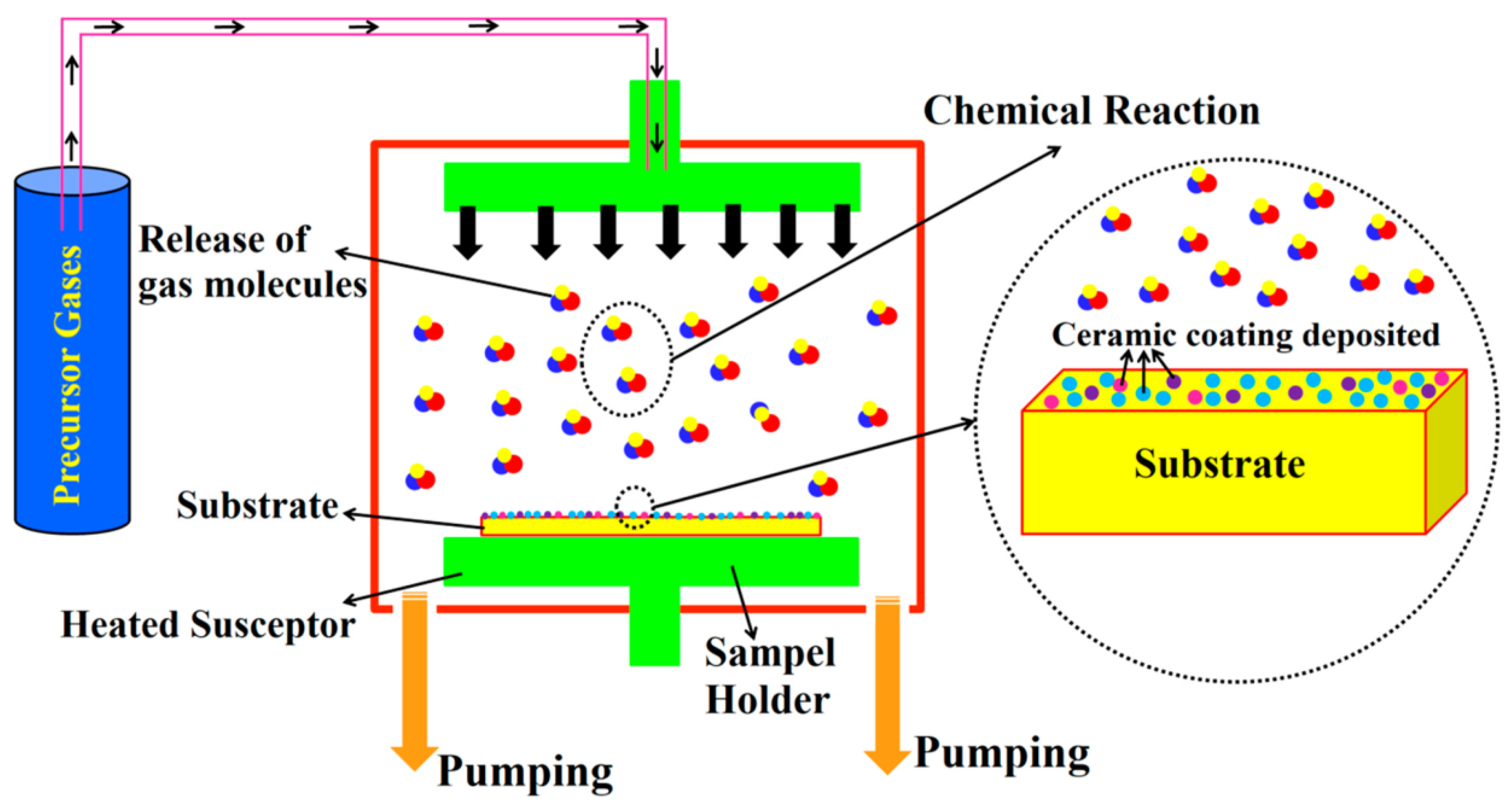
Figure 1. An example of a CVD system for the deposition of ceramic nanocomposite coatings [69].
Crystals 15 01037 g001
Figure 2. (a) Schematic of the AP-CVD setup used to grow 2D TMDCs such as Mo Se2. Optical microscopy images of MoSe2 (b) and W Se2 (c) domain monolayers grown on Si/SiO2. AFM image, height profile along the line marked in the image, and Raman and photoluminescence spectra (dg) of MoSe2 and (hk) of WSe2 [71].
Crystals 15 01037 g002
Figure 3. Schematic diagram of the central part of the home-built UHV-CVD reactor with an optical real-time monitoring system [72].
Crystals 15 01037 g003
Figure 4. The schematic representation of an MW-PECVD process and the steps involved for modification of thin films and membranes [75].
Crystals 15 01037 g004
Figure 5. Commonly used experimental setup for pyrolysis LCVD [76].
Crystals 15 01037 g005
Figure 6. (a) SEM tilt view showcases the nucleation of the nanorods from the sample surface. The arrows indicate the nanorods seeds emanating from the MoS2 film. A growing nanorod is highlighted by the yellow dotted line which could be at its early stage of nucleation and growth. (b) A cross-sectional SEM image of a vertically grown nanorods. Scale bars in (a,b) 200 nm [77].
Crystals 15 01037 g006
Figure 7. (a) A top view SEM image of the grown MoS2 sample (pristine); scale bar 1 μm; a magnified view is shown in the inset; scale bar = 300 nm. (b) Top view SEM image of the same sample after a long-term aging period of ~36 months. The formation of nanorods can be seen over the sample surface. (c) Tilt view of the sample indicating the randomly grown nanorods. Scale bars in (b,c) 1 μm [78].
Crystals 15 01037 g007
Figure 10. SEM images of as-grown MoS2 samples as a function of (TG, TS) for inert gas flow rate ζ = 50 sccm. (a) (775 °C, 145 °C); (b) (775 °C, 140 °C) and (c) (900 °C, 140 °C). Scale bar is 20 μm [86].
Crystals 15 01037 g010
Figure 11. XPS core level Mo3d spectra of MoS2 samples, deposited at different temperatures: 650 °C (a), 750 °C (b), 850 °C (c) and 950 °C (d) [89].
Crystals 15 01037 g011aCrystals 15 01037 g011b
Figure 12. XPS core level S2p spectra of MoS2 samples deposited at different temperatures [89].
Crystals 15 01037 g012
Figure 13. Temperature dependence of the relative concentration of non-stoichiometric MoSx compound estimated from XPS spectra [89].
Crystals 15 01037 g013
Figure 16. Ammonia sensor unit by the four in-line probes method [104].
Crystals 15 01037 g016
Figure 17. Effect on the DC electrical conductivity of (a) PPy and (b) PPy/MoS2 nanocomposites upon exposure to (1000 ppm) ammonia vapors followed by exposure to ambient air with respect to time [104].
Crystals 15 01037 g017
Table 1. Modification techniques.
Chemical Modification Techniques
MethodKey FeaturesApplicationsAdvantagesLimitationsRef.
CVDGas-phase deposition using precursors and reactantsDeposition of CNTs, oxides, anticorrosion coatingsHigh uniformity, good adhesion, high deposition rateHigh temperatures, toxic precursors, high cost[28]
ALDSequential precursor delivery, reaction occurs only on the surfaceNanostructures, membranes, electronicsAtomic-level thickness control, excellent uniformity and conformalitySlow process, expensive and highly reactive precursors[29]
GraftingChemical attachment of functional groups or monomers to the surfacePolymer membranes, improved hydrophilicityIntroduction of new functionalities, high selectivityOnly applicable to functional polymers, scale-up difficulty, high cost[30]
Sol–gelConversion of precursor solutions (metal alkoxides) into oxide filmsPhotocatalysis, filtration, TiO2 membranesSimplicity, porosity control, potential for nanostructuringPossible cracking during drying, sometimes low stability, long process[31]
Physical Modification Techniques
MethodKey FeaturesApplicationsAdvantagesLimitationsRef.
EPDDeposition of charged particles on an electrode under an electric fieldCeramic coatings, membranesFast deposition, uniformity, thickness controlRequires conductive substrate, limited materials[32]
PVD (Physical Vapor Deposition)Vapor-phase reactions at high temperatureCNTs, oxides, anticorrosion coatingsUniformity, high adhesion, fast deposition rateHigh temperature, toxic precursors, high cost[33]
SputteringDeposition of Ar+ ions from a target onto a substrate (PVD)Thin films, electronicsVersatility, low temperature, no precursorsLow deposition rate, expensive equipment, sometimes poor adhesion[34]
Dip coatingImmersion of substrate into solution followed by solvent evaporationPolymer membranes, LbL assemblySimplicity, reproducibility, multilayer capabilityNon-uniform coating, low quality, dependent on conditions[35]
Meyer rod coatingDeposition using a rod (doctor blade)Gas separation membranes, MMMThickness control (100 nm–10 μm), high reproducibilityRequires viscosity optimization, defects at low viscosity[36]
Spin coatingUniform spreading of solution by spinningGO, PDMS membranesSimplicity, low cost, high uniformityOnly for small samples, not scalable[37]
Spray coatingSuspension spraying under pressureCeramic and polymer membranesSimplicity, minimizes pore penetration, no intermediate layerLower permeability, requires viscosity control[38]
Thermal evaporationEvaporation of material in vacuum and deposition onto substrateMetals, organic coatingsSimplicity, cheaper than PVDDifficult for membranes, limited adhesion, non-uniform on complex shapes[39]
Thermal sprayingSpraying molten particles (plasma, HVOF, etc.)Anticorrosion coatings, mechanical protectionHigh deposition rate, coating strengthHigh porosity, low adhesion, requires powerful energy sources[40]
BlendingMixing functional polymers and nanoparticles with a matrixUF/MF membranes, compositesSimplicity, improves hydrophilicity, mechanical strength, antifoulingAffects bulk, not just surface; compatibility issues[41]
Table 2. Modern CVD methods, their variations, advantages, limitations, and applications.
MethodConditions/FeaturesApplicationsMaterials/ExamplesRef.
AP-CVD~1 atm, high deposition rateGraphene devices, turbine blades, electronicsGraphene
zeolite
Al2O3
SiO2
[49]
LP-CVDReduced pressure, heating without carrier gasUniform coatings, membranes, semiconductorsSLG
SiC
Al2O3
MoS2
[50]
HP-CVDPressure > 1 atmSmooth layers, H2-selective membranesSiO2
TMOS
[51]
UHV-CVDExtremely low pressure, low TEpitaxial growth of Si, SiGeSi
SiGe
[52]
AP-PECVDAtmospheric pressure, no vacuumLow-cost coatings, large samplesPolymer layers[53]
DC-PECVDDirect current plasmaCarbon coatings, fuel cellsa-C:H,
steel
[54]
iPE-CVDInitiator at low powerPolymer films, functional coatingsPNIPAAm,
PHEMA
[55]
MW-PECVDMicrowave plasma, high powerBarrier layers, superhydrophobic coatingsSiNx:H,
PDMS
[56]
RF-PECVDPlasma at 13.56 MHzDLC films, PVDF modificationDLC,
PET,
PVDF
[57]
VHF-PECVDFrequency > RF, high deposition rateGas-impermeable coatings, solar cellsSiNx,
Si
[58]
RI-PECVDRadical injection (H)Carbon nanowallsCNWs
Al2O3
[59]
AA-CVDAerosol precursors, ~1 atmUse of non-volatile precursorsOxides, metals[60]
LCVDLaser heating, high rateLocal coatings, mask repairRe, Au, Pt[61]
MOCVDMetal–organic precursors, low TElectronics, corrosion resistanceSnOx:F
Cu
MoS2
Ag
[62]
HFCVDHot filament (2000 °C), H2 + hydrocarbonsDiamond and carbon coatingsDiamond nanoparticles[63]
OCVDMonomer oxidationConductive polymers, sensorsPEDOT
PANI, etc.
[64]
CDCVDDiffusion of precursor and oxidizer toward each otherSilica membrane synthesisSiO2
MoS2
[65]
iCVDRadical polymerization at low TFunctional coatings on polymersPolymer membranes[66]
Table 3. Comparison of LIB performances using different MoS2/carbon materials [114].
StructureElectrode MaterialsFabrication MethodsCapacityRef.
Nanocable websMoS2 + GrapheneUnique side to face contact mode1150 mA h g−1[114]
Core–shell microsphereMoS2 + N-doped carbonOne pot hydrothermal synthesis856 mA h g−1[115]
NanobundleMoS2 + MWCNTDry grinding process using a mortar and pestle1214 mA h g−1[116]
NanobowlMoS2 + CSolvothermal synthesis1164.4 mA h g−1[117]
Flowerlike nanosheetMoS2 + 3D Graphene foamHydrothermal synthesis1127 mA h g−1[118]
Hollow microsphere with onion-like solid nanosphereMoS2 + COne step hydrothermal synthesis1107 mA h g−1[119]
Hierarchical nanofiberMoS2 + active carbon clothSimple dissolution and sintering method971 mA h g−1[120]
Flowerlike networkMoS2 + rGO + MWCNTHydrothermal synthesis1275 mA h g−1[121]
Sandwich like nanosheetMoS2 + N-doped carbonSelf-polymerizing and carbonization process1239 mA h g−1[122]
Nanowires1D−2D NiMoO4 Nanowires + Metallic 1T MoS2 CompositeHydrothermal method using blade and spray coating.941 mA h g−1[123]
NanosheetsVertically aligned 1T-MoS2 on a graphene frameSolvothermal method666 mAh g−1[124]
NanotubesMetallic MoS2Solvothermal method1150 mAh g−1[125]
Disclaimer/Publisher’s Note: The statements, opinions and data contained in all publications are solely those of the individual author(s) and contributor(s) and not of MDPI and/or the editor(s). MDPI and/or the editor(s) disclaim responsibility for any injury to people or property resulting from any ideas, methods, instructions or products referred to in the content.