Raman Spectral Analysis of Sputtered and Sulfurized Nanostructured WS2 Films
Abstract
1. Introduction
2. Materials and Methods
2.1. Preparation of WS2 Films
2.2. Characterization of WS2 Films
3. Results and Discussion
3.1. FESEM Observations
3.2. Raman Spectroscopy
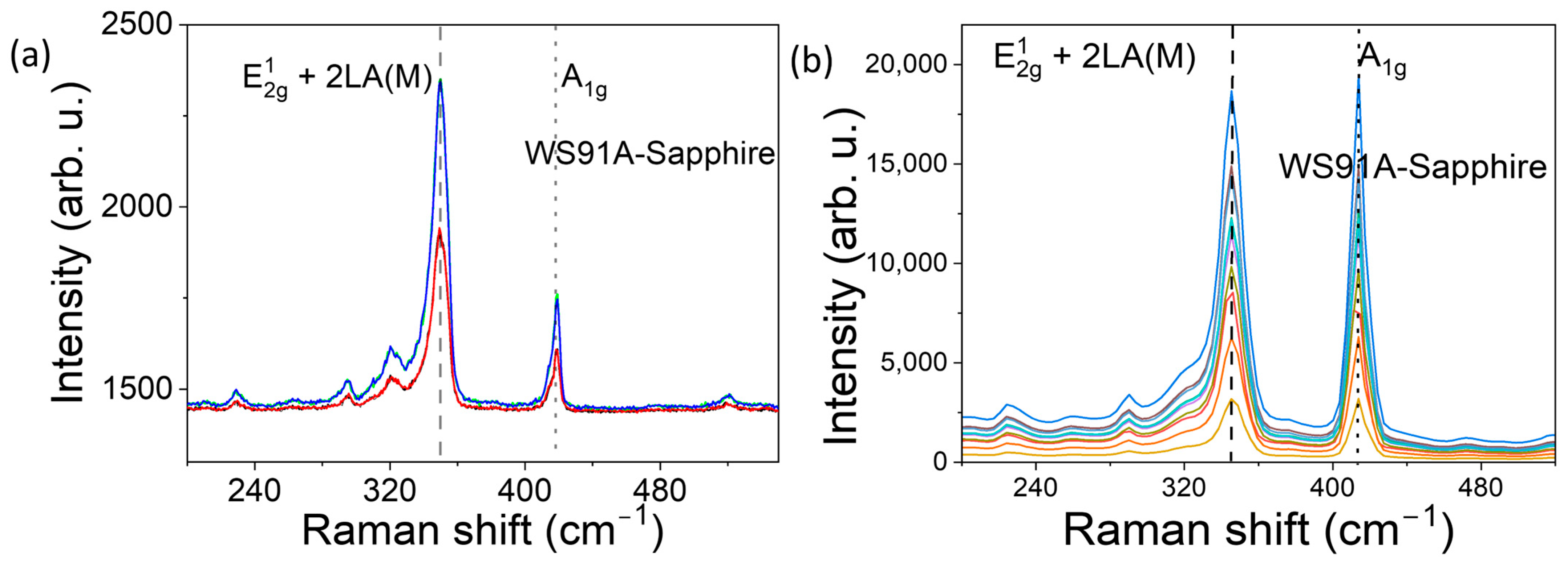
3.3. Analysis of Raman Spectral Characteristics of WS2 Films
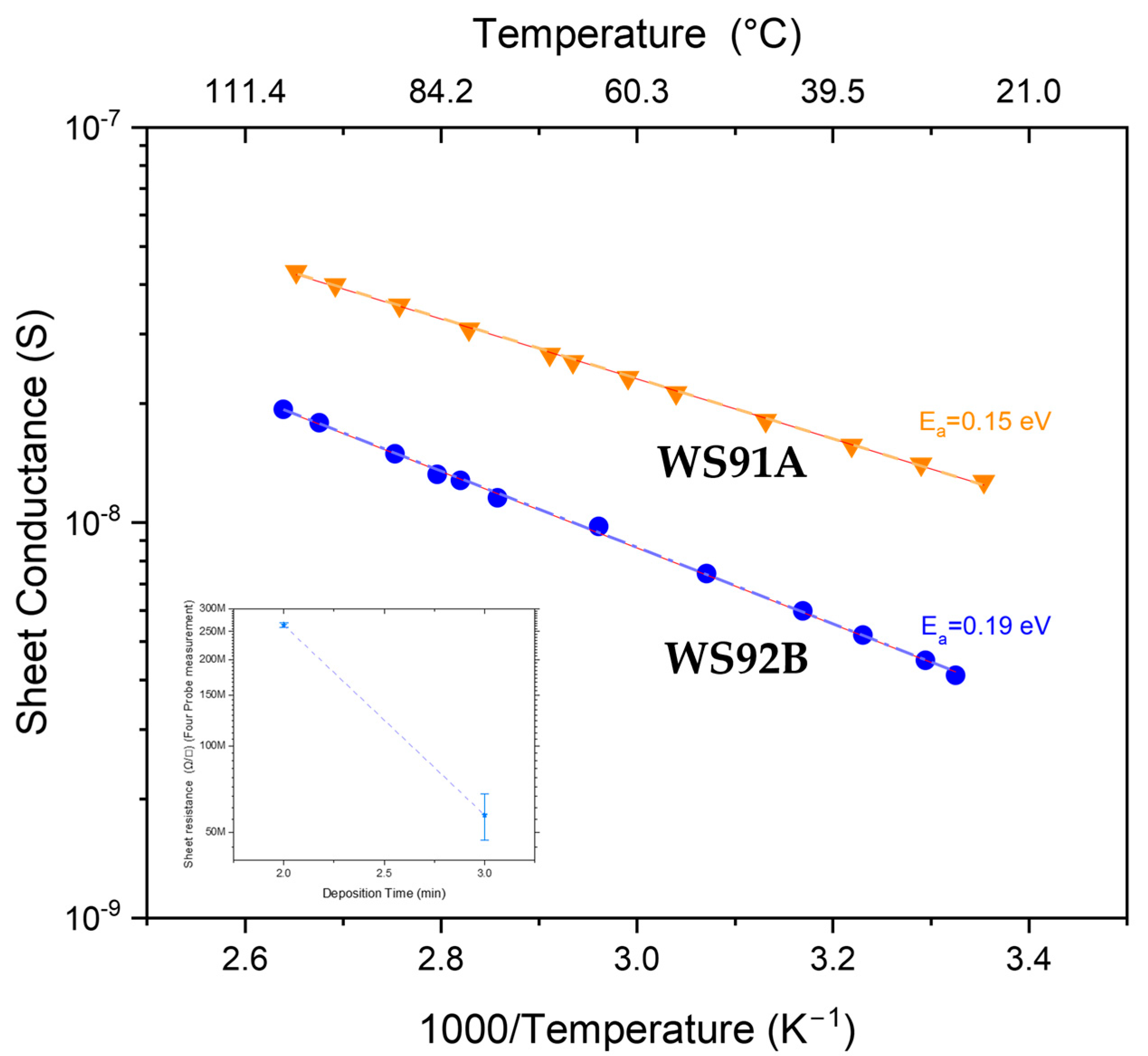
3.4. Electrical Characterization of WS2 Films
4. Conclusions
Author Contributions
Funding
Data Availability Statement
Conflicts of Interest
References
- Berkdemir, A.; Gutierrez, H.R.; Botello-Méndez, A.R.; López, N.P.; Elías, A.L.; Chia, C.; Wang, B.; Crespi, V.H.; Urías, F.L.; Charlier, J.C.; et al. Identification of individual and few layers of WS2 using Raman Spectroscopy. Sci. Rep. 2013, 3, 1755. [Google Scholar] [CrossRef]
- Okeke, C.; Juma, I.; Cobarrubia, A.; Schottle, N.; Maddah, H.; Mortazavi, M.; Behura, S.K. Probing anharmonic phonons in WS2 van der Waals crystal by Raman spectroscopy and machine learning. iScience 2023, 26, 107174. [Google Scholar] [CrossRef] [PubMed]
- Carvalho, B.R.; Pimenta, M.A. Resonance Raman spectroscopy in semiconducting transition-metal dichalcogenides: Basic properties and perspectives. 2D Mater. 2020, 7, 042001. [Google Scholar] [CrossRef]
- Yang, J.; Lee, J.U.; Cheong, H. Excitation energy dependence of Raman spectra of few-layer WS2. FlatChem 2017, 3, 64–70. [Google Scholar] [CrossRef]
- Ahmad, H.; Rashid, H.; Ismail, M.F.; Thambiratnam, K. Fabrication and characterization of tungsten disulphide/silicon heterojunction photodetector for near infrared illumination. Optik 2019, 185, 819–826. [Google Scholar] [CrossRef]
- Zhao, W.; Ghorannevis, Z.; Amara, K.K.; Pang, J.R.; Toh, M.; Zhang, X.; Kloc, C.; Tane, P.H.; Eda, G. Lattice dynamics in mono- and few-layer sheets of WS2 and WSe2. Nanoscale 2013, 5, 9677–9683. Available online: https://pubs.rsc.org/en/content/articlelanding/2013/nr/c3nr03052k (accessed on 1 October 2025). [CrossRef] [PubMed]
- Rajeswaran, B.; Konar, R.; Yitzhari, R.; Nessim, G.D.; Tischler, Y.R. Enhancement of the E12g and A1g Raman modes and layer identification of 2H-WS2 nanosheets with metal coatings. J. Raman Spectrosc. 2023, 54, 1030–1037. [Google Scholar] [CrossRef]
- Peters, L.; Coileáin, C.Ó.; Dluzynski, P.; Siris, R.; Duesberg, G.S.; McEvoy, N. Directing the Morphology of Chemical Vapor Deposition-Grown MoS2 on Sapphire by Crystal Plane Selection. Phys. Status Solidi A 2020, 217, 2000073. [Google Scholar] [CrossRef]
- Smagulova, S.A.; Vinokurov, P.V.; Semenova, A.A.; Popova, E.I.; Vasylieva, F.D.; Obraztsova, E.D.; Fedotov, P.V.; Antonova, I.V. Study of the Properties of Two-Dimensional MoS2 and WS2 Films Synthesized by Chemical-Vapor Deposition. Semiconductors 2020, 54, 454. [Google Scholar] [CrossRef]
- Loginov, A.B.; Ismagilov, R.R.; Bokova-Sirosh, S.N.; Bozhev, I.V.; Obraztsova, E.D. Formation of nanostructured films based on MoS2, WS2, MoO2 and their heterostructures. Tech. Phys. 2022, 92, 2078. Available online: https://journals.ioffe.ru/articles/viewPDF/52225 (accessed on 1 October 2025). [CrossRef]
- Molas, M.R.; Nogajewski, K.; Potemski, M.; Babiński, A. Raman scattering excitation spectroscopy of monolayer WS2. Sci. Rep. 2017, 7, 417. [Google Scholar] [CrossRef] [PubMed]
- Liang, L.; Meunier, V. First-principles Raman spectra of MoS2, WS2 and their heterostructures. Nanoscale 2014, 6, 5394–5401. [Google Scholar] [CrossRef] [PubMed]
- Minezaki, T.; Krüger, P.; Annanouch, F.E.; Casanova-Cháfer, J.; Alagh, A.; Villar-Garcia, I.J.; Pérez-Dieste, V.; Llobet, E.; Bittencourt, C. Hydrogen Sensing Mechanism of WS2 Gas Sensors Analyzed with DFT and NAP-XPS. Sensors 2023, 23, 4623. [Google Scholar] [CrossRef] [PubMed]
- Nicolosi, V.; Chhowalla, M.; Kanatzidis, M.G.; Strano, M.S.; Coleman, J.N. Liquid exfoliation of layered materials. Science 2013, 340, 1226419. Available online: https://www.science.org/doi/10.1126/science.1226419 (accessed on 1 October 2025). [CrossRef]
- Zhang, X.; Tan, Q.H.; Wu, J.B.; Shi, W.; Tan, P.H. Review on the Raman spectroscopy of different types of layered materials. Nanoscale 2016, 8, 6435–6450. Available online: https://pubs.rsc.org/en/content/articlelanding/2016/nr/c5nr07205k (accessed on 1 October 2025). [CrossRef] [PubMed]
- Lee, C.; Jeong, B.G.; Yun, S.J.; Lee, Y.H.; Lee, S.M.; Jeong, M.S. Unveiling defect-related Raman mode of monolayer WS2 via tip-enhanced resonance Raman scattering. ACS Nano 2018, 12, 9982–9990. [Google Scholar] [CrossRef] [PubMed]
- Rao, R.; Kim, H.; López, N.P.; Terrones, M.; Maruyama, B. Interaction of gases with monolayer WS2: An in situ spectroscopy study. Nanoscale 2021, 13, 11470–11477. [Google Scholar] [CrossRef] [PubMed]
- Kim, J.Y.; Gelczuk, Ł.; Polak, M.P.; Hlushchenko, D.; Morgan, D.; Kudrawiec, R.; Szlufarska, I. Experimental and theoretical studies of native deep-level defects in transition metal dichalcogenides. npj 2D Mater. Appl. 2022, 6, 75. Available online: https://www.nature.com/articles/s41699-022-00350-4 (accessed on 1 October 2025). [CrossRef]
- Ci, P.; Tian, X.; Kang, J.; Salazar, A.; Eriguchi, K.; Warkander, S.; Tang, K.; Liu, J.; Chen, Y.; Tongay, S.; et al. Chemical trends of deep levels in van der Waals semiconductors. Nat. Commun. 2020, 11, 5373. [Google Scholar] [CrossRef] [PubMed]
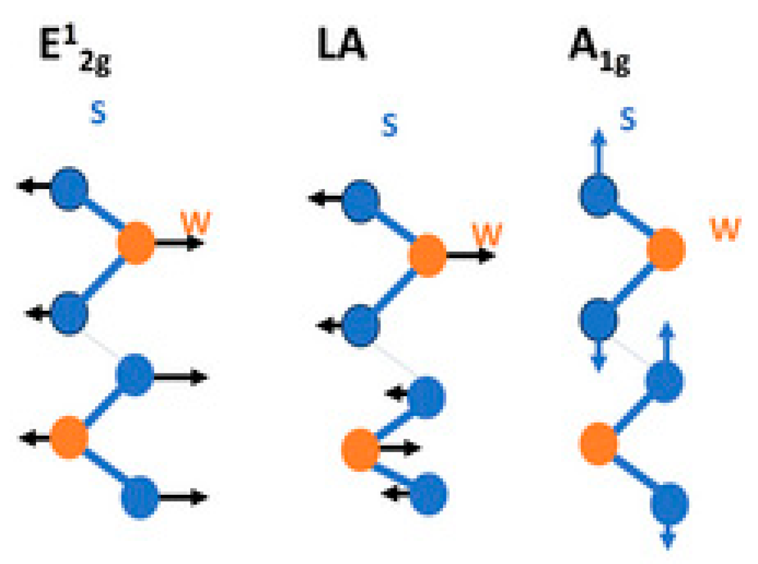
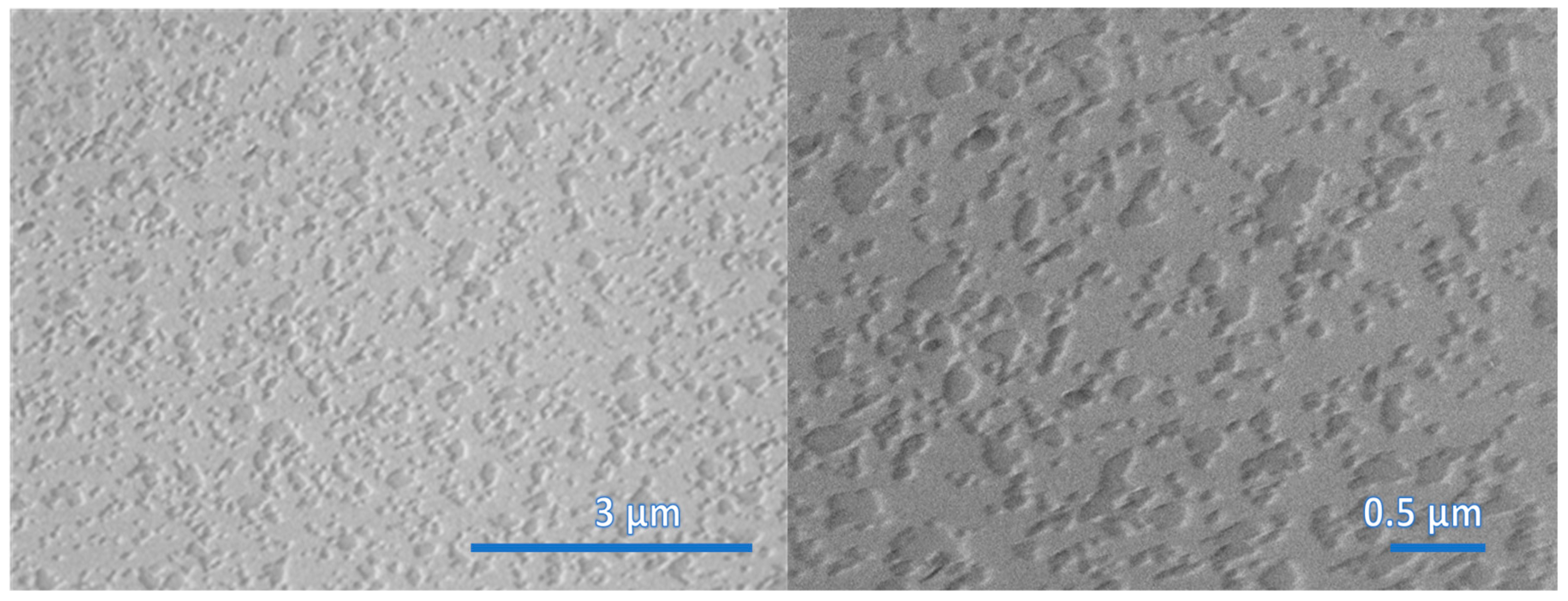
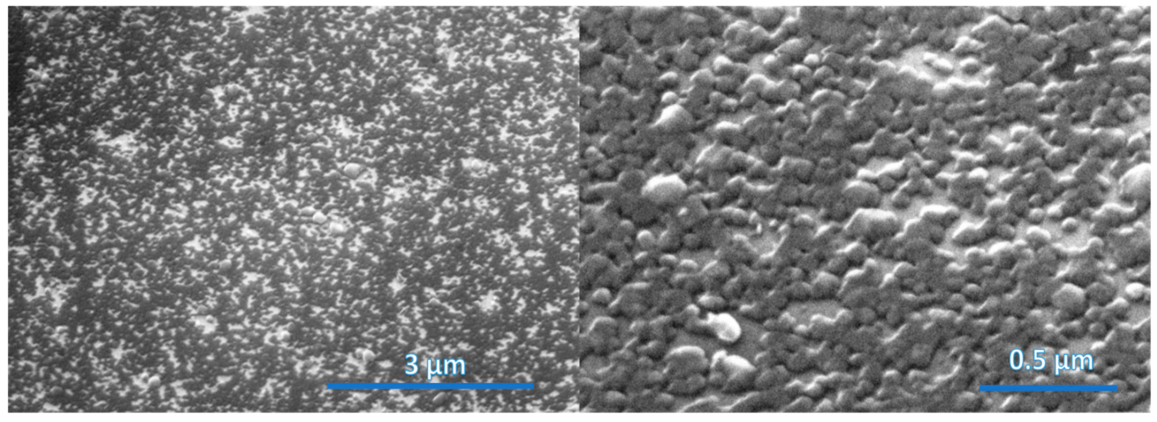
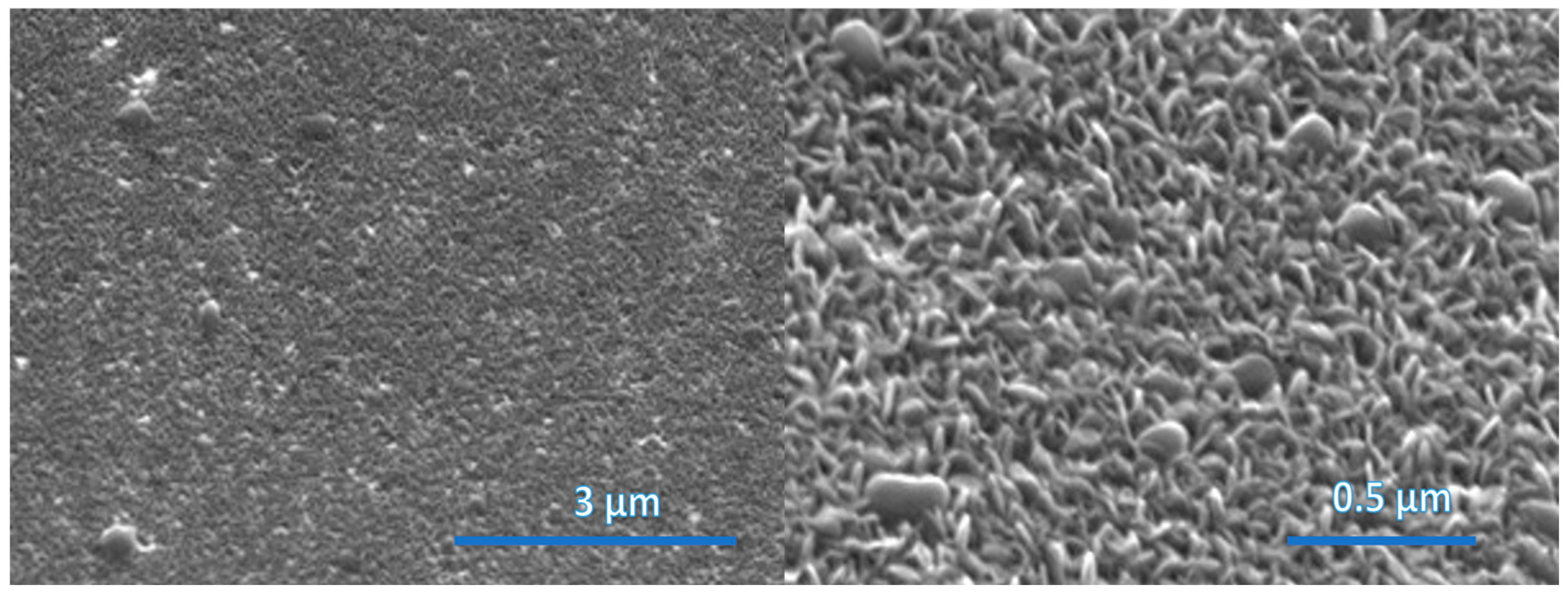


| Identification of WS2 Samples | Magnetron Sputtering Deposition | Sulfurization | |||
|---|---|---|---|---|---|
| Deposition Time | Thickness of Deposited WS2 Film | Sulfurization Temperature | Sulfurization Time | ||
| 1 | WS92A | 1 min | 14 nm | 800 °C | 30 min |
| 2 | WS92B | 2 min | 30 nm | 800 °C | 30 min |
| 3 | WS91A | 3 min | 45 nm | 800 °C | 30 min |
| Identification of WS2 Samples | 532 nm Laser Excitation | |||||
| A1g (cm−1) | FWHM | E12g (cm−1) | FWHM | A1g–E12g (cm−1) | A1g/E12g Intensity Ratios | |
| WS92A | 416.75 | 7.25 | 349.79 | 11.54 | 66.96 | 0.63 |
| WS92B | 416.82 | 6.82 | 349.87 | 11.41 | 66.95 | 0.54 |
| WS91A | 418.20 | 6.30 | 349.28 | 11.19 | 68.92 | 0.76 |
| Identification of WS2 Samples | 632.8 nm laser excitation | |||||
| A1g (cm−1) | FWHM | E12g (cm−1) | FWHM | A1g–E12g (cm−1) | A1g/E12g Intensity Ratios | |
| WS92A | 415.28 | 14.13 | 349.19 | 16.18 | 66.09 | 1.01 |
| WS92B | 413.51 | 11.91 | 346.32 | 14.54 | 67.19 | 1.02 |
| WS91A | 413.74 | 10.22 | 345.22 | 14.39 | 68.52 | 1.04 |
| Identification of WS2 Samples | Deposition Time | Sheet Resistance (Four Probes Method) | Activation Energies (eV) | |
|---|---|---|---|---|
| Mean (Ohm/sq) | Standard Deviation | |||
| WS92A | 1 min | --- | --- | --- |
| WS92B | 2 min | 2.6 × 10⁸ | 0.49 × 10⁸ | 0.19 eV |
| WS91A | 3 min | 5.8 × 10⁷ | 1.06 × 10⁷ | 0.15 eV |
| Identification of WS2 Samples | 532 nm Laser Excitation | 632.8 nm Laser Excitation | Activation Energies (eV) |
|---|---|---|---|
| WS92A | 66.96 | 66.09 | -- |
| WS92B | 66.95 | 67.19 | 0.19 eV |
| WS91A | 68.92 | 68.52 | 0.15 eV |
Disclaimer/Publisher’s Note: The statements, opinions and data contained in all publications are solely those of the individual author(s) and contributor(s) and not of MDPI and/or the editor(s). MDPI and/or the editor(s) disclaim responsibility for any injury to people or property resulting from any ideas, methods, instructions or products referred to in the content. |
© 2025 by the authors. Licensee MDPI, Basel, Switzerland. This article is an open access article distributed under the terms and conditions of the Creative Commons Attribution (CC BY) license (https://creativecommons.org/licenses/by/4.0/).
Share and Cite
Kadlečíková, M.; Hotový, I.; Kumar, N.; Kostič, I.; Sojková, M.; Řeháček, V.; Gregušová, D. Raman Spectral Analysis of Sputtered and Sulfurized Nanostructured WS2 Films. Crystals 2025, 15, 955. https://doi.org/10.3390/cryst15110955
Kadlečíková M, Hotový I, Kumar N, Kostič I, Sojková M, Řeháček V, Gregušová D. Raman Spectral Analysis of Sputtered and Sulfurized Nanostructured WS2 Films. Crystals. 2025; 15(11):955. https://doi.org/10.3390/cryst15110955
Chicago/Turabian StyleKadlečíková, Magdaléna, Ivan Hotový, Naman Kumar, Ivan Kostič, Michaela Sojková, Vlastimil Řeháček, and Dagmar Gregušová. 2025. "Raman Spectral Analysis of Sputtered and Sulfurized Nanostructured WS2 Films" Crystals 15, no. 11: 955. https://doi.org/10.3390/cryst15110955
APA StyleKadlečíková, M., Hotový, I., Kumar, N., Kostič, I., Sojková, M., Řeháček, V., & Gregušová, D. (2025). Raman Spectral Analysis of Sputtered and Sulfurized Nanostructured WS2 Films. Crystals, 15(11), 955. https://doi.org/10.3390/cryst15110955


