Review

Nanoscale Cu2ZnSnSxSe(4−x) (CZTS/Se) for Sustainable Solutions in Renewable Energy, Sensing, and Nanomedicine

by
Sayedmahdi Mohammadi
,
Navdeep Kaur
and
Daniela R. Radu
*
Department of Mechanical and Materials Engineering, Florida International University, Miami, FL 33174, USA
*
Author to whom correspondence should be addressed.
Crystals 2024, 14(5), 479; https://doi.org/10.3390/cryst14050479
Submission received: 21 April 2024 / Revised: 14 May 2024 / Accepted: 16 May 2024 / Published: 19 May 2024
(This article belongs to the Special Issue Semiconductor Nanocrystal Studies for Optoelectronic Applications)

Abstract

:
The importance and breadth of applications of the family of quaternary chalcogenides with the formula Cu2ZnSnSxSe(4−x) (CZTS/Se) where x = 0–4 are steadily expanding due to the tunable optoelectronic properties of these compounds and the Earth abundance of the elements in their composition. These p-type semiconductors are viewed as a viable alternative to Si, gallium arsenide, CdTe, and CIGS solar cells due to their cost effectiveness, Earth’s crust abundance, and non-toxic elements. Additionally, CZTS/Se compounds have demonstrated notable capabilities beyond solar cells, such as photoelectrochemical CO2 reduction, solar water splitting, solar seawater desalination, hydrogen production, and use as an antibacterial agent. Various routes have been explored for synthesizing pure CZTS/Se nanomaterials and significant efforts have been dedicated to reducing the occurrence of secondary phases. This review focuses on synthetic approaches for CZTS/Se nanomaterials, with emphasis on controlling the size and morphology of the nanoparticles and their recent application in solar energy harvesting and beyond, highlighting challenges in achieving the desired purity required in all these applications.

1. Introduction

Fossil fuels, as the dominant energy source, cause permanent and irreversible environmental damage by releasing harmful gases into the atmosphere. Nowadays, attention toward renewable, sustainable energy has increased in parallel with the increasing energy demands and the need to reduce environmental pollution. Among renewable energy technologies, which include geothermal, wind power, and biomass conversion, solar photovoltaics, converting sun light into electricity, carries the most potential, due to the continuous access to the infinite solar resource. Solar cells use the photovoltaic effect to convert solar energy into electricity and have been under development during the last few decades, toward improving their power conversion efficiency (PCE), reducing the cost of production, and satisfying environmental requirements, including sustainability of the fabrication materials and processes [1,2,3,4,5,6,7]. To date, solar cell development and conceptualization has evolved through three generations. The first development, Si-based solar cells, which use crystalline and polycrystalline silicon as the solar absorber and are commercially available, are becoming almost ubiquitous in housing and commercial applications [8,9,10]. However, the large footprint and rigid design of silicon solar panels drove interest in lightweight, flexible substates, as support for the solar absorber, which led to the research and development of thin film technologies, starting with emulating silicon, via amorphous silicon thin film. Discoveries in chalcogenide semiconductors led to exploring materials such as CdTe and Cu(In,Ga)Se2 (also known as CIGS) as solar absorbers, paving the way for the second generation. Thin films made of CIGS or CdTe typically exhibit absorption coefficients two orders of magnitude higher than silicon and have been employed in the fabrication of the p-type absorber layer in the p-n junction architecture [11,12,13,14]. Nanocrystal solar cells, Dye-Sensitized Solar Cells (DSSC), polymer-based solar cells, and halide perovskites solar cells are categorized as third generation solar cells and have leveraged knowledge gained in the nanoscale materials realm [7,15,16].
Within the second generation, the widely used CdTe and CIGS solar absorbers contain toxic elements (Se, Cd) or metals that are expensive or scarce in nature (In, Ga), thus, presenting sustainability concerns [3,6,17,18].
Quaternary semiconductors in the class of Cu2ZnSnSxSe(4−x) (CZTS/Se) where x = 0–4 belong to the I2-II-IV-VI4 group and have been explored as a promising alternative for CIGS materials due to excellent light absorption capabilities, direct bandgaps, and high theoretical efficiency. The constituent elements of CZTS—copper, zinc, tin, and sulfur—are abundant in the Earth’s crust, non-toxic, environmentally friendly, and inexpensive. [3,5,18,19,20,21].
CZTS/Se nanoparticles have been explored to fabricate the absorber layer in thin film PV with high quality and purity toward high-performance PV devices. In addition, nanoscale CZTS/Se with other morphologies, including two-dimensional (2D) nanosheets, one-dimensional (1D) nanostructures, and quantum dots (QDs), have been recently explored for both PV and other applications. QDs which are defined as nanocrystals with diameters less than or equal to the exciton Bohr radius (EBR) of the corresponding bulk material, exhibit quantum confinement, which restricts the motion of the charge carriers causing the semiconductors to behave differently than its bulk counterparts [22,23,24,25]. One-dimensional (1D) nanomaterials such as nanotubes, nanowires, and nanorods offer unidirectional charge transport and scattering properties, which can improve the PCE of the solar cells by enhancing photon absorption, electron mobility, and electron collection. QD solar cells can provide several benefits, such as enhanced charge generation, charge separation, and charge extraction within the single material [7,26].
Due to their sustainable nature, CZTS nanomaterials have recently raised interest in other applications including thermoelectrics [27,28,29,30], photodetection [31], water splitting and hydrogen production [32,33,34], bio–related applications [35], and different types of sensors [36].
CZTS/Se thin films are great candidates for PEC (PEC) CO2 reduction, compared to other semiconductors, due to their favorable conduction band position. Ongoing research efforts are addressing challenges such as slow charge transport, instability issues, and reduced catalytic action in photoelectrical CO2 reduction [37], Among different methods of hydrogen production, generating hydrogen by the PEC water splitting is a promising method to convert solar energy to hydrogen fuel [23,38,39]. The CZTS semiconductor is considered a good photocatalyst candidate due to its good stability, low-cost, and environmental friendliness [40]. CZTS nanocrystal powders have the potential to be used directly for hydrogen production due to the large surface-to-volume ratio of nanoparticles, correlated with the reactivity and large number of accessible catalytic sites [32,33,34]. CZTS QDs can enhance the PEC water splitting reaction through two mechanisms: (i) improving optical properties and (ii) aiding in charge carrier separation and transfer [23]. The highest photocurrent density obtained was found to be 1.82 mA/cm2 at 1.23 V/RHE for CZTS QDs/hematite graphene thin film. The work revealed that the presence of CZTS QDs increased light absorption in the water splitting application [24]. Recently, CZTS was used in a Pt/A-TiO2/CdS/CZTS photocathode employed in seawater desalination showing superior stability and an average rate of salt removal of 0.46 μg cm−2 min−1. After 500 h of cyclic desalting, the photocathode still maintained more than 95% of its original desalination performance [41].
The tunable optical properties of CZTS QDs, such as broad-band absorption, narrow-band emission, tunable size, and large surface-to-volume ratio, make them an attractive candidate in sensing biological molecules and cells for bio-related applications, especially when coupling QDs with molecules [35,42]. CZTS QDs capped with 1-octadecanamine deposited onto fluorine doped tin oxide (FTO) glass has been reported as a novel electrocatalytic material for a non–enzymatic glucose sensor [35]. Ceylan et al. worked on a tissue engineering application of CZTS QDs by the loading of QDs into membranes. They developed wound dressing scaffolds with antimicrobial properties by using CZTS QDs to stop wound infections, suggesting that CZTS QDs-integrated membranes have potential applications as antimicrobial layers for the purpose of wound healing [43]. Kumar et al. explored the antibacterial activity of the synthesized tube-shaped CZTS NPs towards Gram-positive and Gram-negative bacteria, demonstrating that the synthesized CZTS particles exhibited strong antibacterial activity, equivalent to that of Ag NPs and ampicillin [44]. CZTS NPs also exhibit antimicrobial activity against Bacillus cereus, Pseudomonas aeruginosa, and Legionella pneumophila subspecies pneumophila [45]. Polyether sulfone (PES) membranes modified with 20–30 nm CZTS NPs exhibit high antimicrobial activity against six bacterial strains and one fungal strain revealing the surface protection properties of the CZTS NPs and their concentration-dependent antioxidant activity.
CZTS NPs were further investigated for cancer therapy. The proapoptotic and antiproliferative activities on human lung adenocarcinoma A549 cells were reported for the first time by Colak et al. The findings suggested that the apoptotic effect was caused by the formation of reactive oxygen species (ROS) on CZTS NPs surface [46].
Tang et al. harnessed the microwave absorption properties of CZTS nanocrystals (CZTS NCs) for their application as microwave-susceptible agents for tumor eradication. The report revealed that CZTS NCs have the ability to produce singlet oxygen under a low-frequency microwave field, which is in tumor photodynamic therapy (PDT) [47].

1.1. CZTS/Se Structure and Properties

CZTS exists in three tetragonal crystal structures: stannite, kesterite, and PMCA (pre-mixed CuAu), which differs based on the metal cations position within the tetrahedral voids on the positions of Cu and Zn (Figure 1). Stannite structure (space group I 4 ¯ 2 m, and b = 5.403 Å and c = 10.932 Å) evolves from (001) oriented CuAu and kesterite (space group I 4 ¯ , a and b = 5.443 Å and c = 10.786 Å) from (201) oriented chalcopyrite [3,19,21,48,49]. The kesterite structure is the most thermodynamically stable phase for CZTS. Distinguishing between stannite, kesterite, and PMCA structures by using X-ray diffraction (XRD) is challenging due to the isoelectronic nature of Cu+ and Zn2+. Synchrotron, neutron diffraction X-ray, and Raman spectroscopy are suitable techniques for this purpose because of the disparity in neutron scattering lengths of copper (bCu = 7.718(4) fm) and zinc (bZn = 5.680(5) fm) [50,51,52]. The melting point of bulk CZTS is 990 °C with a molar mass of 439.471 g.mol−1 and a density of 4.57 g.cm−3 [6]. The bandgap of CZTS/Se is in the range from 1.0 eV to 1.5 eV depending on the S/Se ratio, which is also close to the ideal value of 1.4 eV for single junction semiconductor solar cells. Additionally, it has a strong absorption coefficient of ~104 cm−1 [21,53,54].

1.2. CZTS Phase Diagram

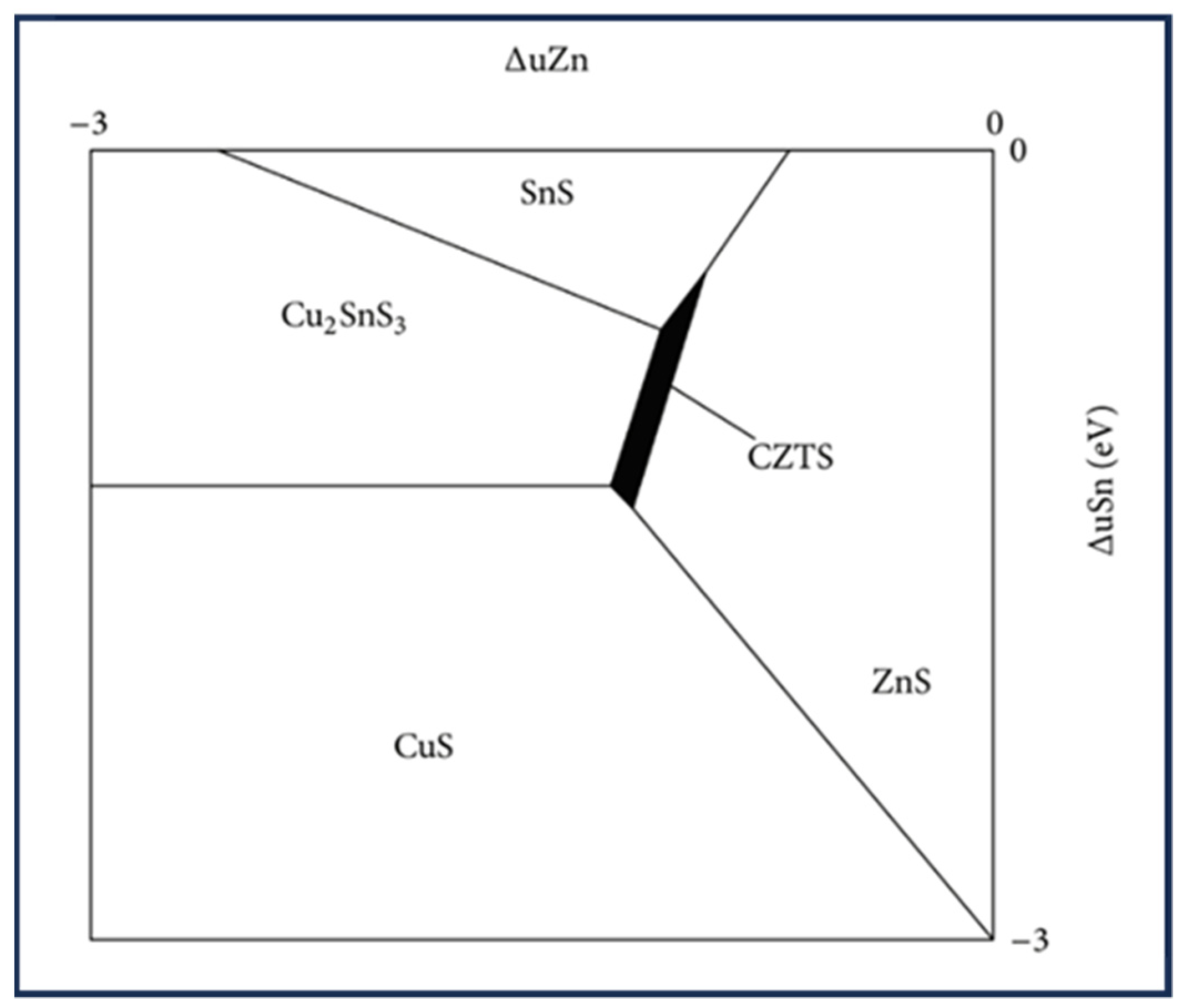
The coexistence of phases, such as ZnS/Se, CuxS/Se, SnSx/Sex, or Cu2SnS3/Se3 with the quaternary CZTS/Se phase in the solar absorber layer can drastically reduce the efficiency and performance of solar cells; therefore, the phase stability and control of defects formation are critical in processing CZTS materials [55,56,57]. Phase equilibrium studies revealed that the single-phase stannite CZTS exist in a very small range of component deviation (1–2%) below 550 °C [58,59]. Understanding the nature of the defects is necessary to control the synthesis process toward less impurities and defects. Due to the narrow region of chemical potential between 1 eV and 0.1 eV that is favorable for the formation of the quaternary phase of CZTS, as shown in Figure 2, synthesizing single-phase kesterite poses significant challenges [19,55].
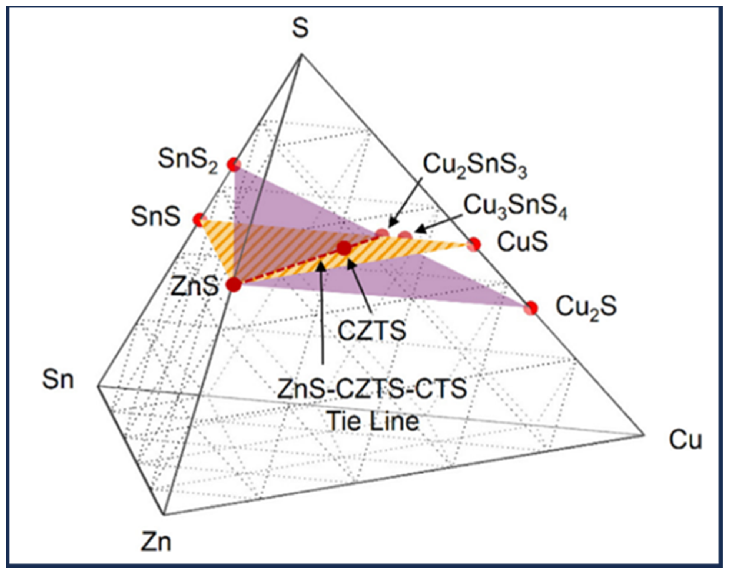
Kesterite is reported as a more thermodynamically stable phase than stannite and PMCA. This is because it has a smaller strain energy, lower Madelung energy, larger bandgap, and is more negative [49]. It is likely that the ZnS impurity phase will exist in Zn-rich and Cu-poor regions, as shown in Figure 3, phase diagrams where the kesterite phase region is shifted to the ZnS–SnS boundary [55,60]. Lafond et al. identified four off-stoichiometry types formed by defect complexes incorporated in a kesterite CZTS structure via modeling based on the charge balance and reported the compositional ability and flexibility of the kesterite phase to deviate from stoichiometry (Cu:Zn:Sn = 2:1:1) [61]. For CZTS phase equilibria, the pseudo-ternary phase diagram is typically referred to as shown in Figure 3. The compounds ZnS, CZTS, and Cu2SnS3 meet at a common point along the tie line. The Cu2S-ZnS-SnS2 plane retains the formal oxidation states of the metals in the kesterite structure and the CuS-ZnS-SnS plane maintains a consistent ratio of metal: S [62].
Considering the complex phase structures of CZTS materials, the necessity for tuning their structural, morphological, and optical properties based on their broader application regime at nanoscale holds great significance.

2. Nanoscale CZTS/Se Material: Synthesis Approaches

This present review concentrates on all the nanoscale synthesis methods for CZTS involving both top-down and bottom-up approaches. To the best of our knowledge, there is no current review focused on nanoscale CZTS and related derivatives. Methods and technologies that yield nanoparticles, including nanosheets, nanorods, and QDs, are discussed in detail, with additional focus on thin film fabrication, specifically those that are either formed of nanoscale precursors or present nanostructure upon fabrication with other methods. The research findings focusing on various aspects of CZTS materials are summarized in Table 1 and are explained thoroughly in the text, given that many processes and applications bear similarity to some extent, from fabrication methods [3,5,19,55,63], the life cycle assessment (LCA) and green synthesis approaches [3,64], to applications [3,6], and efficiency and properties improvement [3,5,6,65].

2.1. Hydrothermal Method

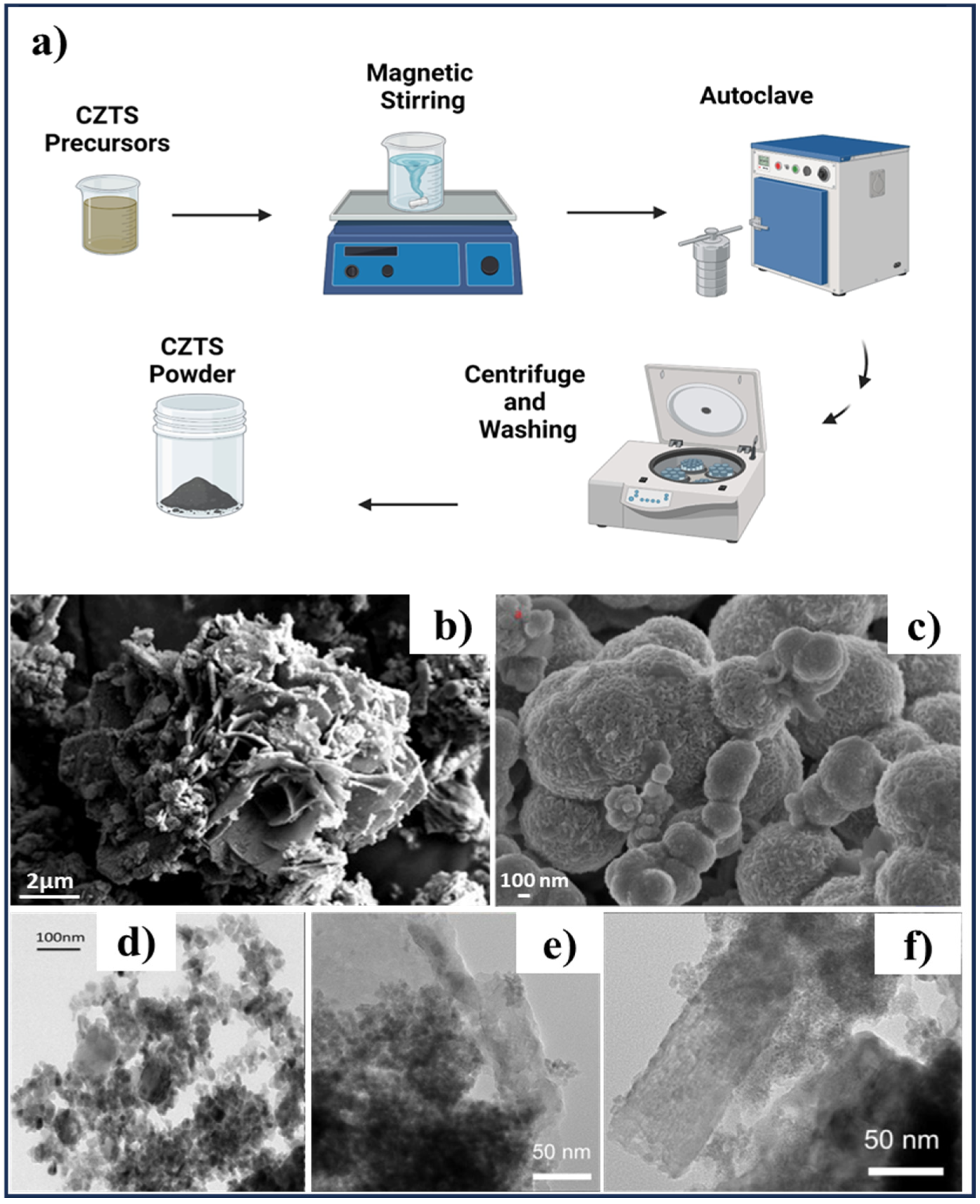
Hydrothermal synthesis is the process of synthesizing materials by conducting chemical reactions in a sealed autoclave, which is heated above ambient temperature and pressure. Typically, crystal growth occurs in an autoclave, a steel pressured vessel, using water as solvent and is usually carried out at the temperatures below supercritical temperatures of water (374 °C) [95,96]. A sequence of the hydrothermal process for synthesizing CZTS NPs is shown in Figure 4a. Camara et al. was the first to utilize the one-step hydrothermal method using coper (II) chloride (CuCl2·2H2O), zinc dichloride (ZnCl2), tin dichloride (SnCl2·2H2O), and sodium sulfide (Na2S·9H2O) precursors to synthesize CZTS nanoparticles (Figure 4d). It was reported that optimizing the concentration ratios of sulfur and copper aids in good crystallinity and fine-tuning the optical properties of CZTS resulting in improved absorption spectra [66]. Recently, Liu et al. synthesized the CZTS powders with the hydrothermal method using metal chlorides, SeO2 as a selenium precursor, and hydrazine hydrate as the reduction agent at 160–200 °C and investigated the effect of reaction times on final product. It revealed that the hydrothermal process caried out at 200 °C for 90 h conditions provided well-crystallized Cu2ZnSnSe4 nanosheets without Se impurities having irregular polygon flake morphology with a thickness of ~30 nm–40 nm and 50 nm–200 nm diameters [72]. Synthesis of the kesterite CZTS nanoparticle by a hydrothermal process using Cu, Zn and SnCl2, and Na2S was reported by Vanalakar et al. who investigated the effect of reaction time on the CZTS nanocrystal structure and its properties. They reported synthesis of CZTS nanoparticles with a diameter of 20–30 nm after performing hydrothermal processing at 220 °C for 24 h [67]. Akshaya et al. reported the synthesis of CZTS QDs with a 10.74 nm and 12.2 nm crystallite size by hydrothermal method (Figure 4c) using cupric chloride dihydrate (CuCl2.2H2O), zinc chloride (ZnCl2), stannous chloride dihydrate (SnCl2.2H2O), and thiourea (CH4-N2S) as the precursors with a molar ratio of 2:1:1:8, respectively [68].
Sheebha et al. synthesized CZTS with a hierarchical flower-like morphology depicted in Figure 4b through hydrothermal method by dissolving CuCl2, ZnCl2, SnCl2, and thiourea in distilled water [69]. Henríquez et al. investigated the photocatalytic properties of synthesized CZTS nanoparticles through the photodegradation of Congo red azo dye solution under light irradiation using a solar simulator. Synthesized CZTS nanoparticles exhibited average sizes ranging between 7 nm and 60 nm with different nanocrystal shapes (rod-shape and spherical) seen in the high-magnification TEM images (Figure 4e,f) [70]. Cristóbal-García et al. conducted hydrothermal processing to synthesize CZTS nanoparticles using Zn(NO3)2·6H2O, CuSO4, SnCl2·2H2O, and CH4N2S precursors. Precursors were added into the solution of PVP and ethylene glycol, and the final solution was stirred at 70 °C for 30 min. CZTS nanoparticles with the domain size between 5 and 6 nm were achieved [71].
The hydrothermal method offers an efficient and cost-effective approach to produce CZTS nanomaterials under conditions that do not require a protective atmosphere or refluxing, with the temperature and pressure within the vessel being highly adaptable. Moreover, it enables control over the composition, purity, size, shape, and surface area of synthesized nanoparticles, along with dispersion through the fine-tuning of process variables such as precursor concentration, reaction temperature and duration, and pH level. Nevertheless, scaling up production through the hydrothermal method presents challenges, as it necessitates high temperatures and pressures, prolonged heating periods, and substantial energy consumption, which in turn, increase the overall production costs [3,4,69,70,97].

2.2. Solvothermal Method

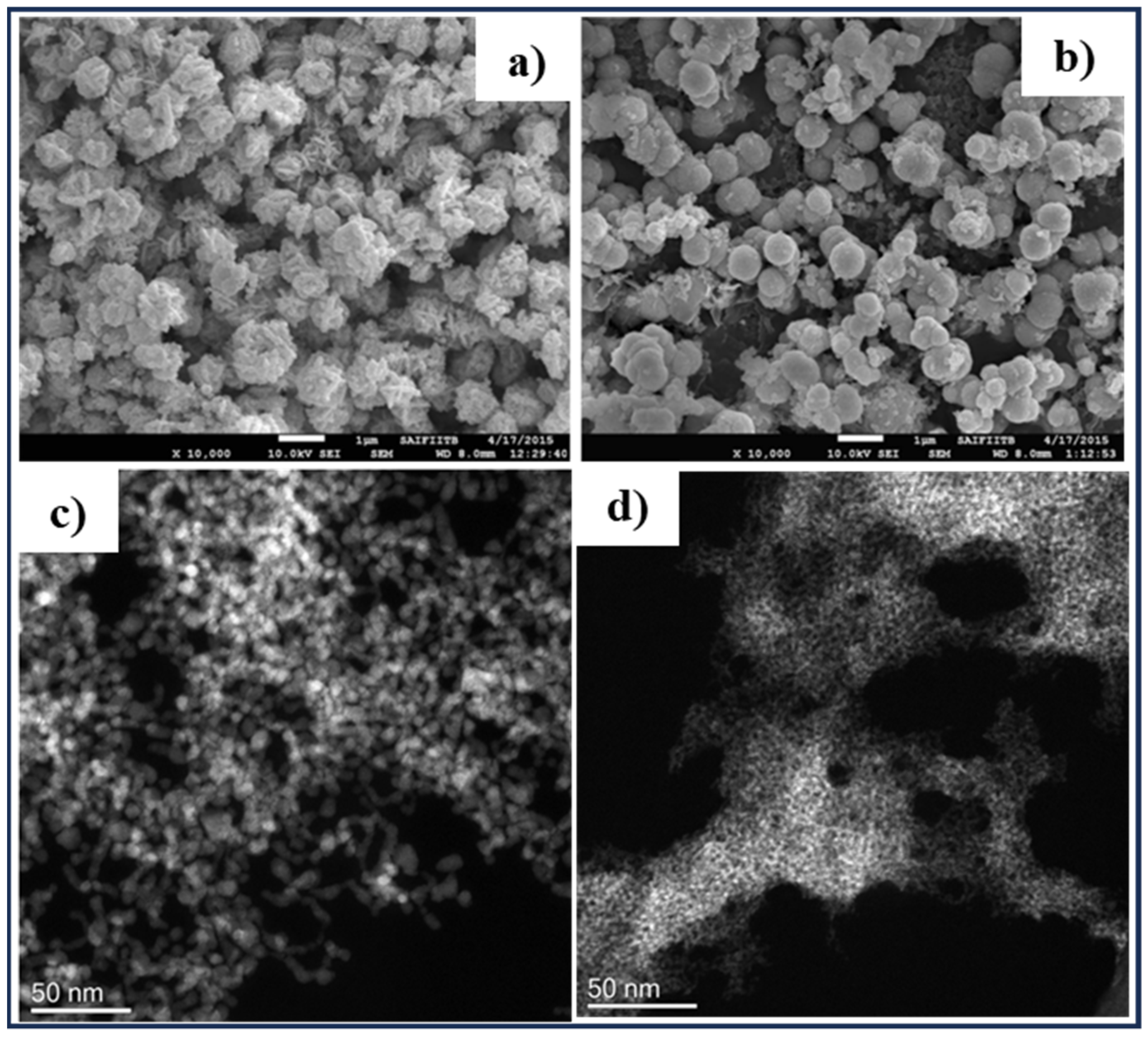
Solvothermal synthesis is similar to the hydrothermal method with similar mechanism and preparation steps to synthesize CZTS compounds (Figure 4a) [96,98]. Solvothermal synthesis involves a chemical reaction occurring in a solvent at an elevated temperatures (usually 100–1000 °C) and pressures in an autoclave. Any organic or inorganic solvent can be used in a solvothermal synthesis. The high temperature and pressure facilitate the dissolution of the chemical reagents and the growth of the crystallized materials. In recent decades, several research groups have utilized solvothermal methods to synthesize CZTS nanomaterials. Yan et al. synthesized CZTS nanocrystals with a size of 6–9 nm from chlorides of Cu, Zn, Sn, thiourea, and ethanol by solvothermal process and investigated the impact of different temperatures (160 °C, 180 °C, and 200 °C) and reaction times (6 h to 24 h) [73]. Patro et al. investigated the effect of synthesis parameters, such as reaction temperature, time, and precursor concentration on the phase, crystallinity, and morphology of CZTS nanoparticles synthesized by microwave-assisted solvothermal method [74]. It has been reported that the morphology of the nanoparticles changes from being flower-like to sphere-like (Figure 5a,b) when the Zn/Sn precursor concentration is changed from 2 mM to 10 mM [74]. Ahmad et al. synthesized CZTS nanoparticles under solvothermal conditions using different metal salt precursors (acetates and chlorides), and carbon disulfide as the sulfur source. It is reported that CZTS synthesized from chlorides under 2 h at 250 °C conditions, which shows the particles with an ellipsoidal to spherical shape growing from a mean size of 7 to 15 nm, respectively (Figure 5c). On the other hand, the CZTS sample synthesized from acetate precursors at the same temperature and time (Figure 5d), shows a particle size of 2–3 nm [75].
The direct synthesis of CZTS on FTO substrate by solvothermal method was reported by Wei et al. using copper (II) chloride dihydrate, zinc (II) chloride, tin (II) chloride dehydrate, thiourea, hexadecyl trimethyl ammonium bromide (CTAB) and oxalic acid. In a typical experiment, the precursors were dissolved in ethanol and magnetically stirred, and placed in a Teflon liner with a well-cleaned FTO substrate to proceed with the solvothermal process at 200 °C for 24 h, resulting in thin film with spherical particles containing nanocrystals of 11–12 nm in diameter [76]. Cao et al. synthesized poly-dispersed CZT (S.Se) nanocrystals with size of 8–12 nm by solvothermal method using CuCl, ZnCl2, SnCl4·5H2O, and Se powders in ethylenediamine solution [77].
The fabrication of CZTS nanomaterials with various crystal sizes, morphologies, and shapes is achievable using solvothermal methods. The solvothermal method produces homogenous and high-purity nanoparticles, which do not require post-synthesis annealing processes. In this method, particle size and shape can be easily controlled by process parameters such as pH, temperature, time, and solvent composition. However, long-time reactions are perceived as a disadvantage of this method [3,76,97,99,100].

2.3. Sol–Gel Method

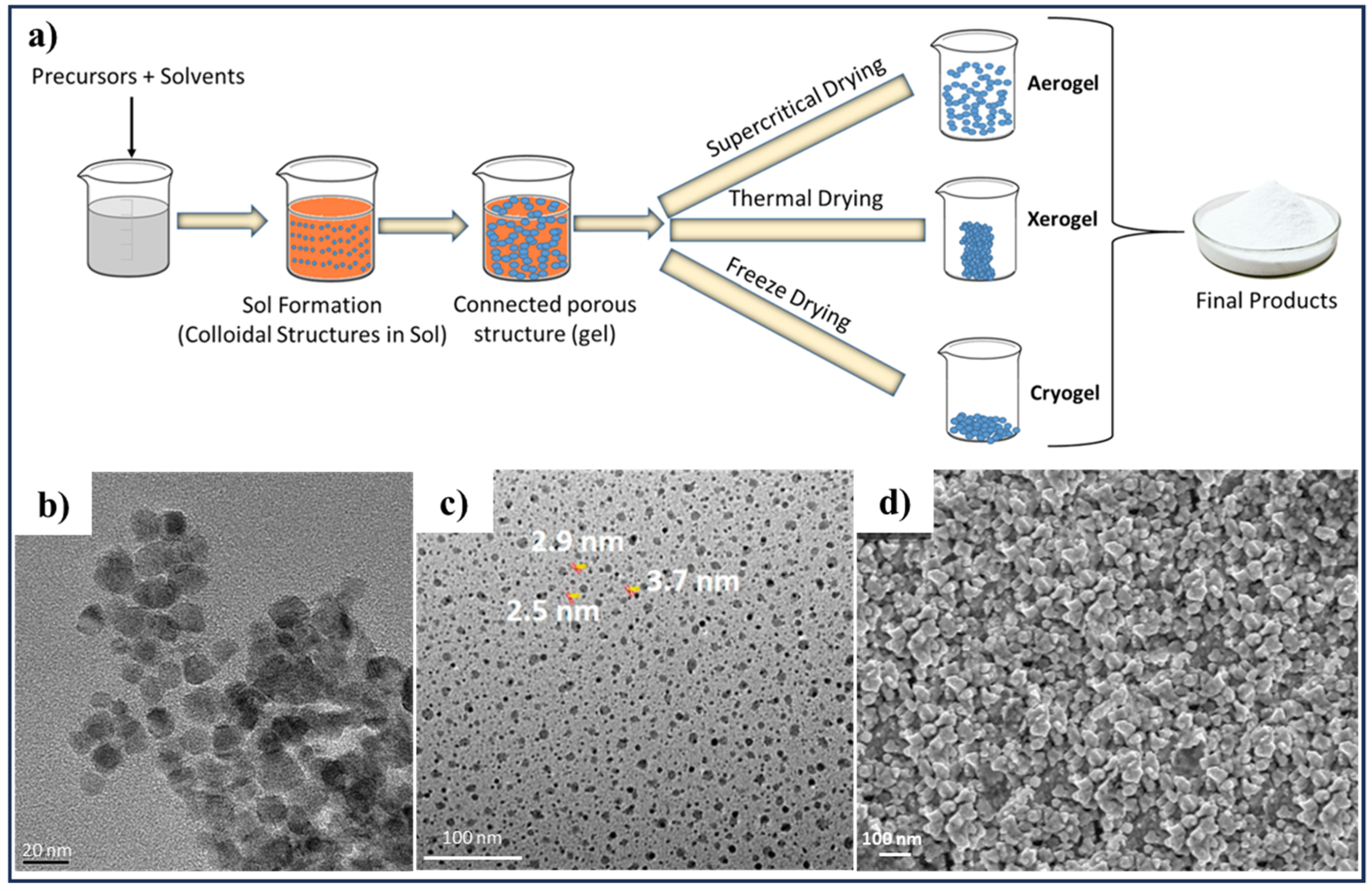
The sol–gel method constitutes several chemical reactions resulting in a liquid and a solid phase by using a colloidal solution (sol) that gradually develops into a gel-like network. The first attempts at creating silica gels using the sol–gel synthesis method date back to the middle of the 1800s [101]. Generally, sol–gel synthesis is divided into two types: aqueous where water is used as a reaction medium and non-aqueous with organic solvent as a reaction medium [102]. Schematics of the steps involved in the sol–gel method are depicted in Figure 6a [103]. Several studies have been reported conducting aqueous and non-aqueous sol–gel methods to fabricate CZTS compounds [56]. The synthesis of CZTS nanocrystals by hot-injection method from copper (II) acetylacetone, zinc (II) acetate, tin (II) chloride, and sulfide powder under argon was reported by XIA et al. The estimated crystalline size of about 10–20 nm was reported and seen from TEM image (Figure 6b) [78]. Khushaim et al. reported the fabrication of stoichiometric CZTS thin films by the sol–gel method using a spray deposition technique, and avoiding a toxic S or H2S sulfurization atmosphere. CZTS precursor solution was prepared from CuCl2·2H2O, ZnCl2, SnCl2·2H2O, with CH4N2S as the S source, at slightly elevated temperature (50–60 °C) with stirring to ensure proper mixing. TEM images (Figure 6c) confirmed the presence of the nanoparticles with sizes in the range of 2–4 nm [79]. Orletskyi et al. demonstrated the CZTS films with an average crystallite size of 60 nm (Figure 6d) synthesized by the spin coating of non-toxic dimethyl sulfoxide (DMSO)-based sol–gel in low vacuum (0.1 Pa) [80].
Hence, sol–gel is a well-established method for synthesizing high-quality CZTS nanomaterials offering advantageous control over size, texture, and surface properties, easy implementation, low-cost, and large surface area production [102]. However, the uncontrolled porosity of growing layers and the time-consuming process are its significant drawbacks [56]. The sol–gel method might involve toxic solvents and hazardous chemicals which are undesirable for scaling-up and reproducibility, and extensive research is being conducted to resolve these problems by using aqueous and non-toxic chemicals [104,105]. The synthesizing of single-phase CZTS thin films by sol–gel is difficult because of the formation of secondary phases such as CuxS, ZnS, and SnS, along with non-uniformity of the grains. However, alternative approaches such as microwave-assisted synthesis have been reported to help overcome some of these challenges [106,107,108].

2.4. Co-Precipitation Method

In the co-precipitation method, multiple compounds precipitate from a solution at the same time (Figure 7a). Fabrication of CZTS nanocrystals without any sulfurization and selenization has been reported using the co-precipitation method which is less toxic to the environment compared to other chemical methods. Wong et al. developed a route for the selective synthesis of wurtzite CZTS nanocrystals in the range from 8 nm to 10 nm diameters by using thiourea as a sulfur source. In that study, wurtzite CZTS nanocrystal was synthesized by the mixing of copper (II) acetate, tin (IV) acetate, zinc acetate, thiourea with diethanolamine, and stirring the mixture for a while under N2 atmosphere at room temperature. Based on the TEM images (Figure 7b), the average diameter of 10 ± 1.1 nm for the wurtzite CZTS nanocrystals was estimated as having a direct bandgap energy of 1.56 eV [81]. Pal et al. used the co-precipitation method to synthesize wurtzite CZTS nanocrystals (NCs) at room temperature using cupric (II) chloride, zinc (II) acetate, and tin (II) chloride. Thiourea was used as the sulfur anion source and water as a solvent without any surfactants, noble gases, and vacuum process. Thiourea was used as a sulfur precursor in three concentrations (20 mmol, 18 mmol, 16 mmol) to investigate its effect on the final CZTS powders and reported improvement in crystal growth by increasing sulfur content. XRD, Raman, and SEM characterizations confirmed that the sample with 18 mmol of thiourea reveals better morphology with the average crystallite size of 17 nm, compared to 16 mmol and 20 mmol of thiourea (Figure 7c) [82].
The co-precipitation method is a straightforward, low-cost, and high production yield process. Using a relatively low temperature, it results in the easy control of particle size and composition of materials. On the other hand, pH impact, agglomeration, poor crystallinity, and size uniformity are certain drawbacks of this method [3,109].

2.5. Hot-Injection and Colloidal Synthesis Methods

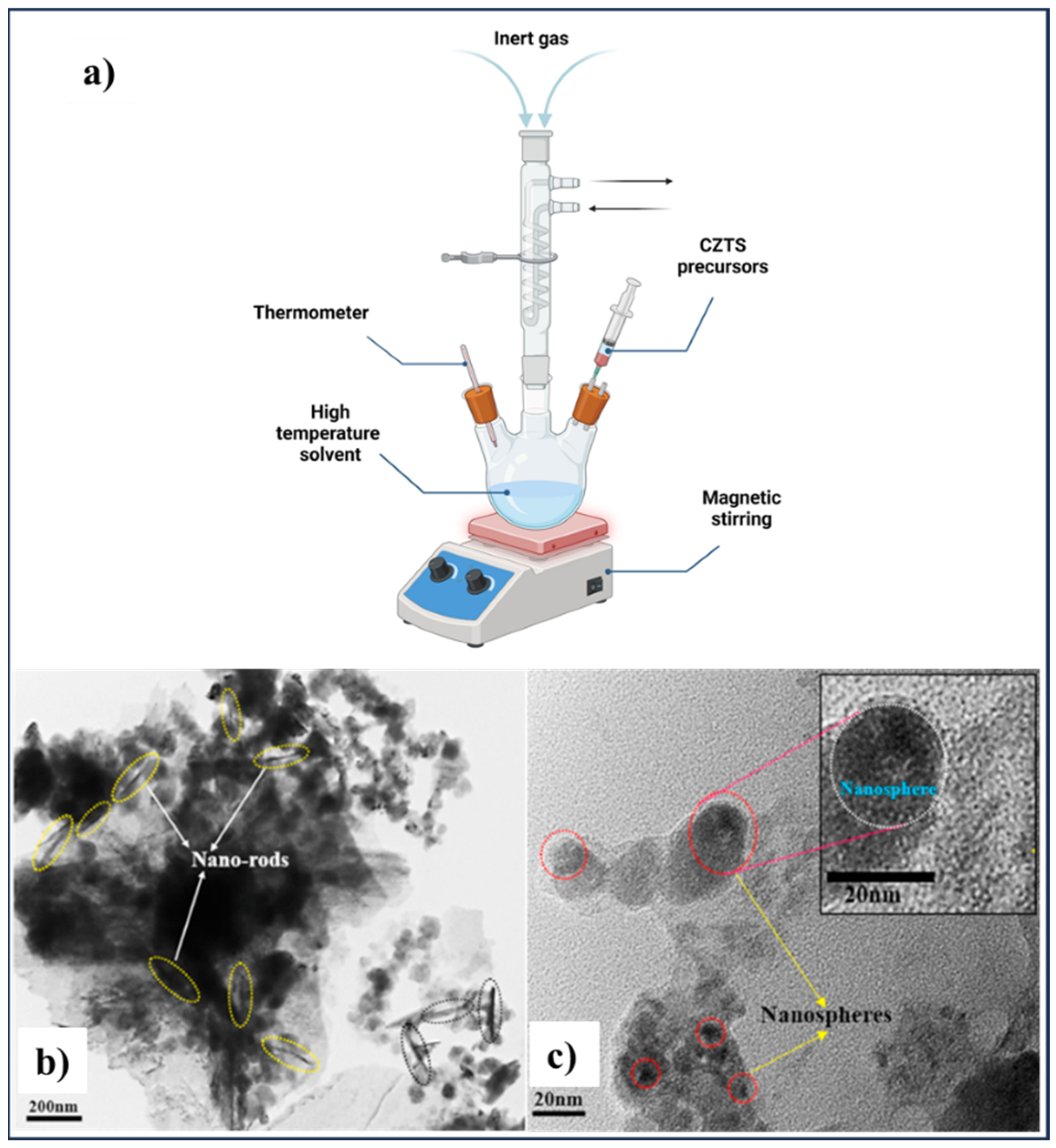
The hot-injection method was first used to synthesize cadmium chalcogenide nanocrystals in 1993, and was followed by the application of this technique to the synthesis of other types of nanocrystals, including metal oxides and semiconductors [110,111]. As evident from its name, hot-injection process reactions occur in the liquid phase by injecting precursor solutions into another solution of precursors or in a solvent that is kept at an elavated temperature, typically over 250 °C (Figure 8a). CZTS nanocrystals prepared by the hot-injection method are popular in solution processable solar cell technology since their desirable chemical and physical properties make them ideal for thin film deposition using dip-coating, inkjet printing, spraying, or roll-to-roll coating under ambient conditions [84,112]. This method can enable the cheap and scalable fabrication of uniform nanoparticle thin films for solar cells, and allows controlled composition, phase formation, and uniform morphology [111]. Cao et al. demonstrated the use of a novel solution processed synthesis approach to obtain CZTS and CZTSSe thin films offering easy control over the metal ratios. The precursors are binary and ternary Cu, Zn, and Sn sulfide nanoparticles, in various combinations, for example, ZnS combined with Cu2SnS3, at stoichiometric ratios, to create the thin film precursor layer, which is then converted to CZTSSe through annealing in the presence of selenium. Solar cell devices fabricated with this method exhibited a high PCE of 8.5%. Further optimization focuses on refining the metal and S/Se ratios, controlling the bilayer formation, and improving the back contact for enhanced device performance [113]. Semalty et al. prepared CZTS nanoparticles with a size of 2–5 nm through the colloidal hot-injection method by using different ligands for the application of the photocatalytic degradation of hazardous water pollutants. In that report, single-phase kesterite structured CZTS was synthesized from copper (II) chloride dihydrate, zinc (II) chloride, tin (IV) chloride, and S powder as precursors. Copper, zinc, and tin precursors were added to a two-neck round bottom flask with Trioctylphosphine oxide (TOPO) in temperatures between 250 and 300 ºC for an hour. After changing the color from yellow to orange, elemental S with Trioctylphosphine (TOP) was rapidly injected into the flask and maintained at a temperature of 230 ºC for 20 min; the pale brown color was seen, and after heating it up to 250 °C, a deep black color was obtained. TEM charactrization of as-synthesized CZTS nanoparticles revealed the agglomerated nanorods (120–140 nm) with a fringe width of 0.23 nm for that sample which was synthesized using TOPO and TOP as the ligands (Figure 8b), and nano spherical morphology (diameter of 15–35 nm) with a fringe width of 0.2–0.4 nm for the sample with n-butylamine and octadecene as ligands (Figure 8c) [83].
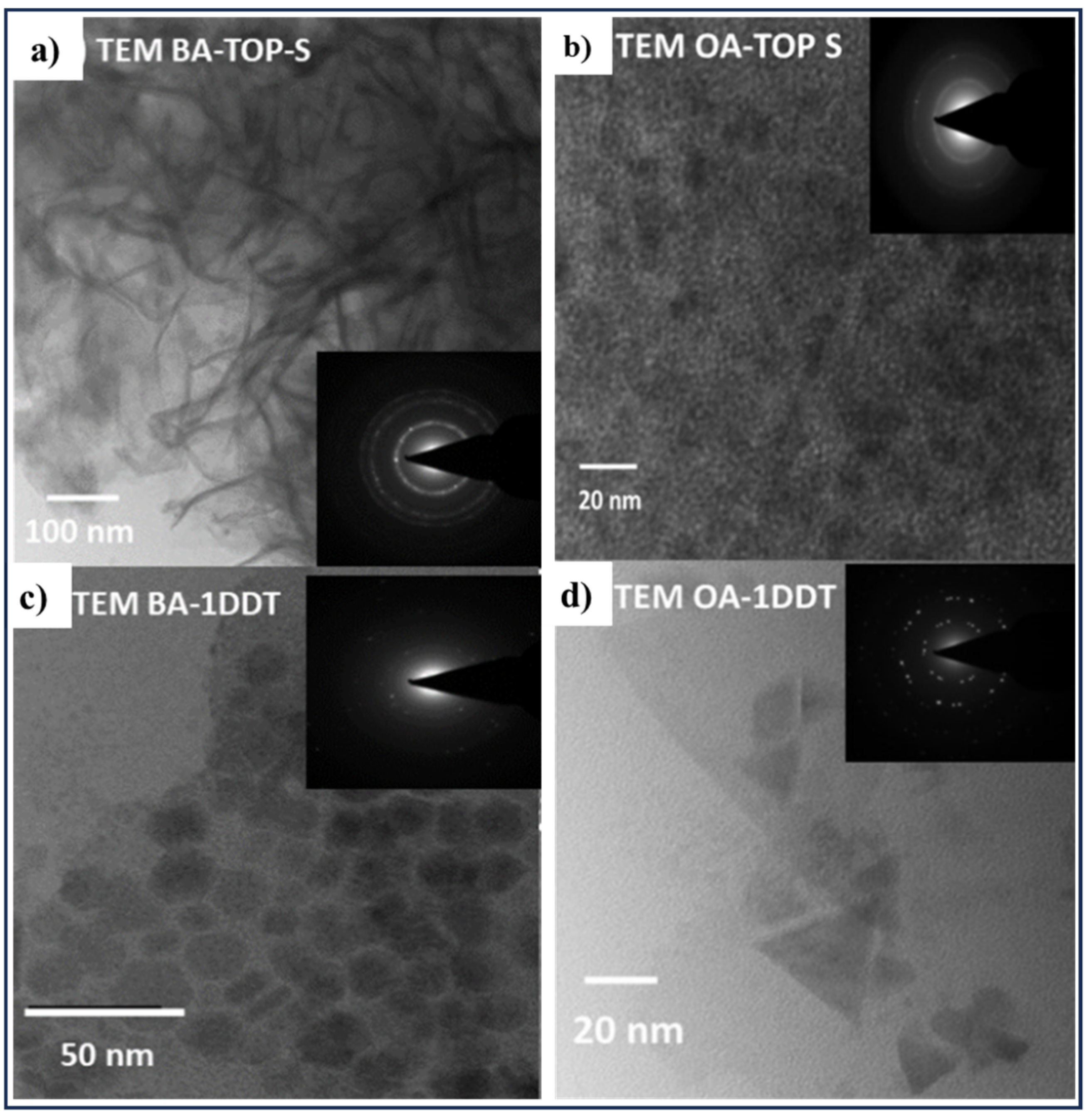
Synthesis of kesterite and wurtzite CZTS nanocrystals with average size of 4–9 nm, using thioacetamide as the sulfur source, and oleylamine (OLA) as both the solvent and the nanocrystal stabilizer, was reported by Méndez-López et al. The effect of synthesis time on the structural, morphological, compositional, and optical properties, along with the reduction of the wurtzite phase by increasing reaction time was reported [84]. Mirbagheri et al. reported the synthesis of a single-phase, ligand-free CZTS nanoparticles with an average diameter of 23 ± 11 nm, which can be dispersed in polar solvents to produce nanoparticle ink for solar cell thin film fabrication [85]. Jain et al. studied the effect of various capping ligands and sulfur sources on the shape, structure, and properties of pure phase kesterite CZTS nanocrystals using the hot-injection method. Copper (II) chloride dihydrate (CuCl2.2H2O), zinc (II) chloride (ZnCl2), and tin (IV) chloride (SnCl4) were used as precursors with different capping ligands such as butylamine (BA) and oleic acid (OA), and 1-Dodecanethiol (1-DDT) and Trioctylphosphine-S (TOP-S) as the sulfur sources. Hot injection was performed at 275 °C for 15 min. The TEM results (Figure 9a–d) show the formation of CZTS nanoparticles with different morphology. Using BA as the capping ligand produces thin plates with hexagonal symmetry, while OA produces triangular-shaped nanoparticles [86]. The same research group carried out another study on the malachite green photocatalytic degradation by CZTS rod-shape nanoparticles synthesized through the hot-injection method using different Zn/Sn precursor ratios (Zn:Sn ratio as 1.2:1 2:1 and 4:1) while keeping other conditions and all precursor ratios constant. In that study, copper (II) chloride dihydrate (CuCl2·2H2O), zinc (II) chloride (ZnCl2), tin (IV) chloride (SnCl4), and S powder were used as the precursor and Trioctylphosphine oxide (TOPO)/Trioctylphosphine (TOP) as capping agents. A best in case degradation rate of 1.7 × 10⁻² min−1 was observed for an organic dye malachite green in sunlight for CZTS nanoparticles with a Zn:Sn ratio of 2:1 (compared to Zn:Sn ratio of 2:1) [87].
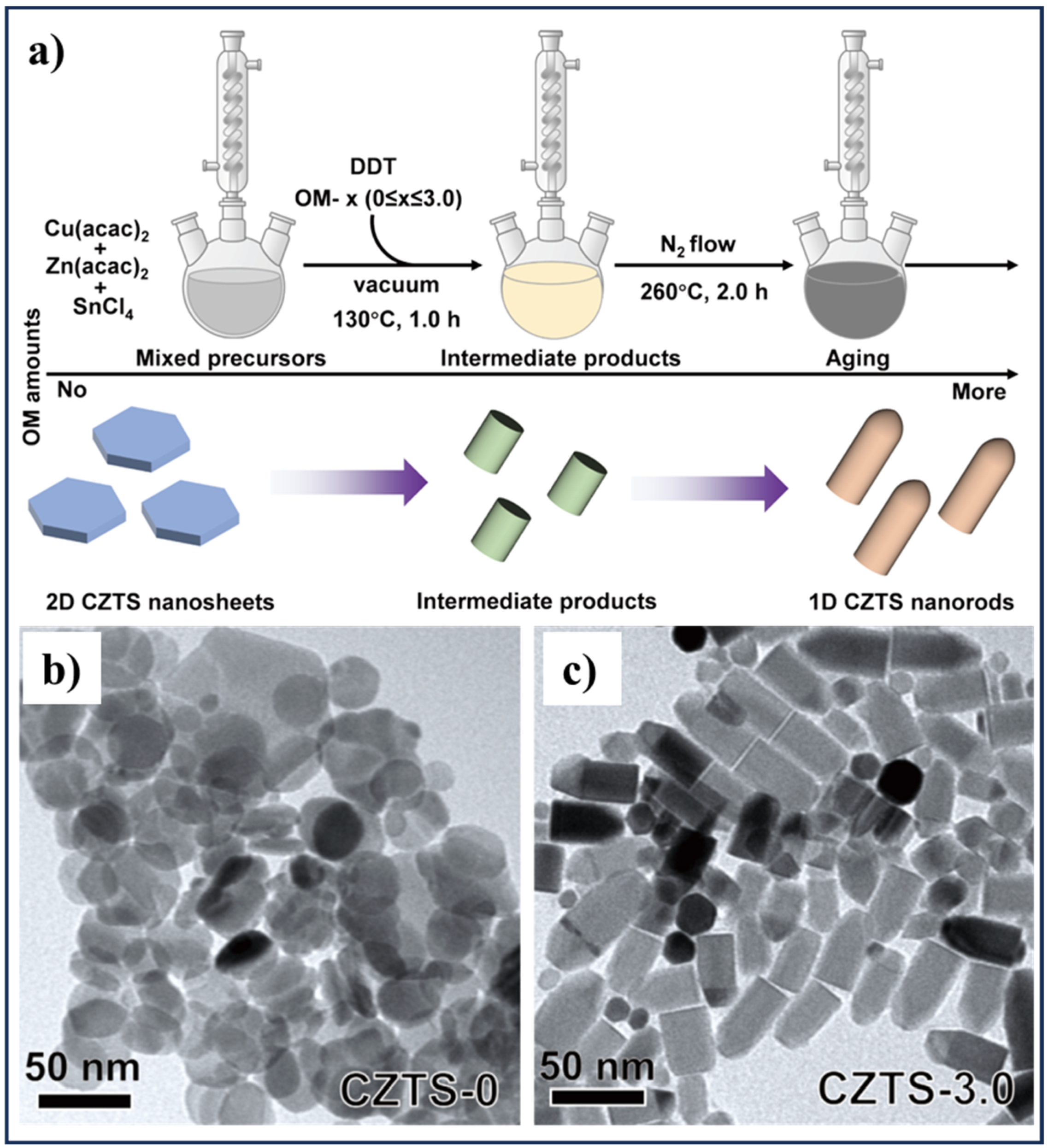
Li et al. reported the evolution of CZTS nanocrystals from 2D nanosheets to 1D nanorods using a one-pot colloidal synthesis method which was assisted by the continuous addition of oleylamine (OM) as a surfactant (Figure 10a). The report describes the process of synthesizing CZTS nanosheets using metallic salt precursors including Cu(acac)2, Zn(acac)2, SnCl4, and 1-dodecanethiol (DDT), followed by adding the ligand solvent OM to the reaction system. A thin layer structure of 2D hexagonal nanosheets with the average hexagonal nanosheets diameter of 31.8 ± 6.9 nm (Figure 10b) was reported for the synthesized sample without adding OM(CZTS-0), and by adding 3.0 OM to the reaction, a gradual transformation of CZTS nanocrystals from nanosheets to nanorods occurred (Figure 10c) [88]. Prabhu et al. used the hot-injection method to synthesize the Cu2ZnSn(SxSe1−x)4 (x = 0.0, 0.4, 1.0) nanoparticle quanternary compounds. They reported that the selenium doping resulted in the increasing of nanoparticle grain size (Figure 11a–c), and a compact morphology was obtained with nearly stoichiometric composition [89].
A low-temperature solution-phase synthetic approach to prepare stand-alone CZTSSe nanosheets was reported by Mohammadnezhad et al. The process is a cascade synthesis of CZTSSe starting from SnSe2 nanosheets, synthesized via a hot-injection method using 1-dodecanethiol as a morphology directing reagent [112]. SnSe2 nanosheets served as a templating lattice and were further reacted with Cu salts using the hot-injection method to render Cu2SnSe3. Ultimately, Zn(S2NEt2)2 was reacted with the Cu2SnSe3 to form the CZTSSe which, remarkably, retained the nanosheet morphology. The CZTSSe nanosheets were deposited on fluorine-doped tin oxide (FTO) substrates and used as counterelectrode in DSSC solar cells which resulted in a power conversion efficiency of (5.73%), which is comparable to the values obtained using Pt-based CE (5.78%) [112].
Thus, the hot-injection method facilitates a straightforward one-pot synthesis process for creating CZTS nanomaterial structures through the sequential injection of precursors. It employs a process that operates at relatively high temperatures and incorporates a surfactant during synthesis. However, scaling-up this method to produce large quantities of samples poses significant challenges [3].

2.6. Solid State, Mechanical Alloying, and Mechanochemical Synthesis Method

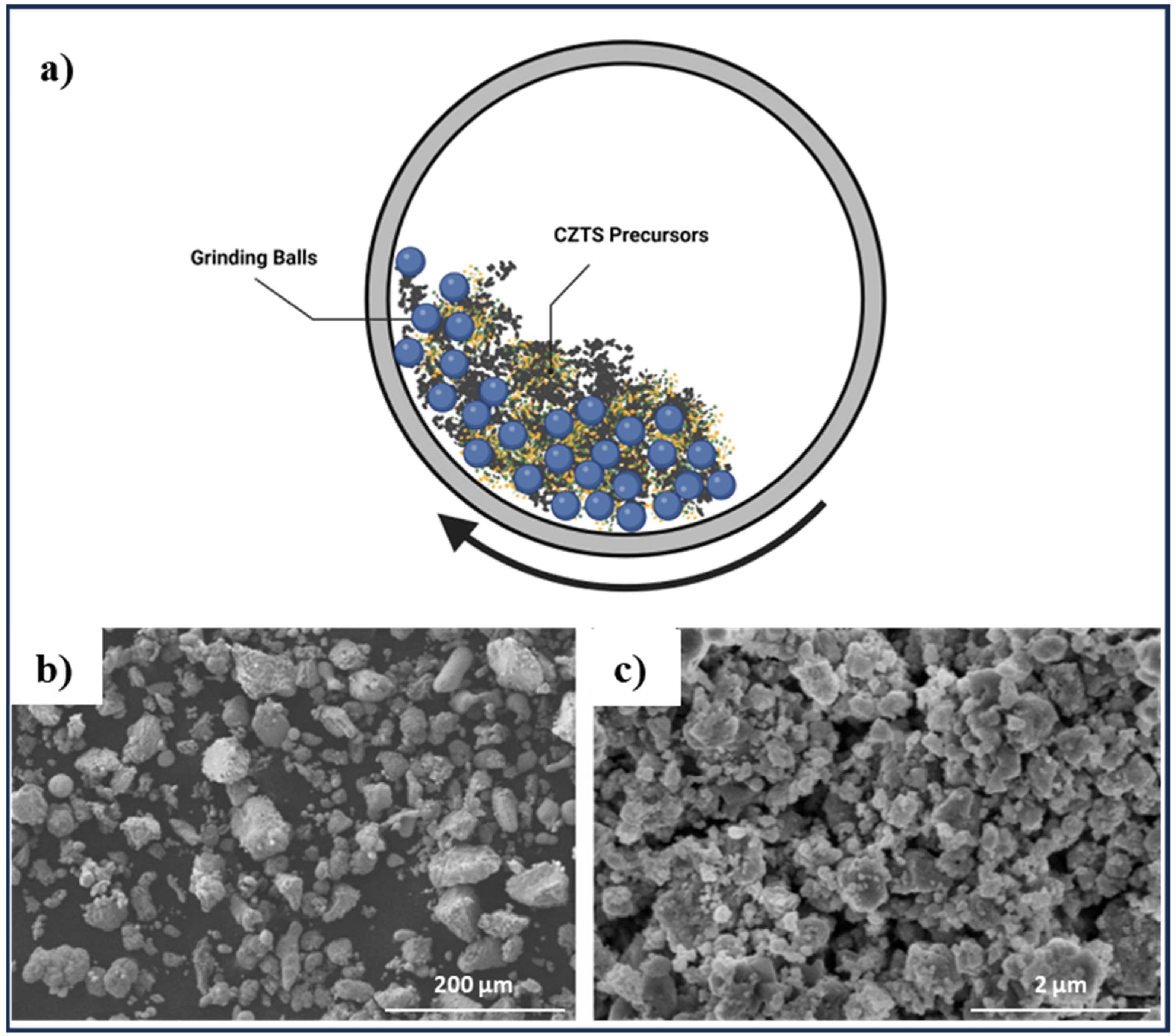
Mechanical alloying, known as a mechanically induced solid-state reaction, is a complex physical and chemical process which involves consecutive steps of welding and fracturing by a high-energy ball mill or rod mill [114,115]. The process starts with the mixing of powders in needed portions and loading them into the mill with grinding balls (Figure 12a). The milling process will continue for the desired lengths of time [116]. The synthesis of CZTS nanomaterials using the mechanical alloying method was first reported by Wang and Gong by conducting the planetary ball milling of elemental precursors for 25 h [90]. Zhou and Wang prepared CZTS microparticles for screen printing paste by a four-step method; sequentially: wet ball milling, isostatic pressing, sintering, and wet ball milling [117]. Long et al. reported the synthesis of CZTS nanoparticles with particle distribution in the range of 50–60 nm, using the mechanical alloying method from Cu, Zn, Sn, and S powders after 16 h of milling. It was reported that the CZTS phase was obtained after 12 h of milling and the single phase of CZTS was formed after 16 h [30].
Pareek et al. worked on the synthesis of CZTSe and CZTS nanocrystalline powders with a particle size distribution in the range of 133–286 nm, from elemental metal and chalcogen powders using ball milling at low temperatures. They reported the formation of pure phase kesterite for both CZTS and CZTSe [91]. Isotta et al. reported the synthesis of nanocrystalline CZTS from the elemental components in stoichiometric proportions, with a grain size between 10 and 20 nm, using a high-energy planetary mill. A subsequent sintering process at temperatures ranging from 560 °C to 660 °C was employed to achieve a stable tetragonal phase of CZTS [27]. Suha et al. adopted a mechanochemical process to fabricate CZTS nano-powders and inks. In that research, Cu, Zn, Sn, S, and butanol were ball-milled at 450 rpm for 30 h to obtain a homogenous mixture of single-phase CZTS nano-powder [92]. A single-step solution-based solid-state reaction process was utilized by Mokurala et al. for the synthesis of single-phase CZTS equiaxed nanoparticles with approximate size of 10–15 nm using acetates of Cu, Zn, thiourea, and tin chloride as precursors. In that study, precursors (Cu:Zn:Sn:S) in a molar ratio of 2:1:1:8 were mixed and milled with ethanol, and the homogenized precursor solution was synthesized in a tubular furnace at 250 °C for 1–12 h in an argon atmosphere. FEG-SEM (Figure 12b) and FEG-TEM (Figure 12c) reveal CZTS equiaxed nanoparticles with a particle size of 10–15 nm which is synthesized at 250 °C for 1 h [93]. Agnes et al. synthesized the nanocrystalline solid-state synthesis and e-beam evaporation growth of Cu2ZnSnSe4 by the dry ball milling method at various milling times, to investigate the behaivior of single-phase and secondary phase formation. A crystal size of 10–20 nm was reported [94].
These methods have some unique advantages such as simple equipment, cost effectiveness, easily designed components, reliability, alloying materials with high-melting temperatures, and fit for mass production. However, there are some great challenges such as contamination of powders by milling balls or rods [114].
The synthesis of the CZTS nanoparticles can be achieved through various methods. In this review, the papers we searched each portrayed methods with distinct precursors, mechanisms, and outcomes that influence the properties of the final product such as impurities, secondary phases, morphology, particle size, and shape. In addition, from an environmental perspective, several factors such as energy consumption, waste generation, and hazardous chemical use come into play.
Each method has its specific advantages and limitations, influencing its suitability for different applications. The hydrothermal method is notable for its efficiency and adaptability, allowing precise control over the properties of nanoparticles without the need for a protective atmosphere, making it excellent for lab-scale production but challenging to scale up due to high energy and operational costs. Solvothermal synthesis shares similar benefits, providing fine control over particle characteristics through adjustable process parameters such as pH, temperature, and solvent composition, though it also suffers from issues related to long reaction times. On the other hand, the sol–gel method offers ease of implementation and low-cost operation, excelling in controlling size and texture but is hindered using potentially toxic solvents and the difficulty in avoiding secondary phase formations, which compromises scalability and reproducibility. Comparatively, the co-precipitation method stands out for its simplicity and low-cost factors, yielding high production rates at relatively low temperatures, yet it is limited by problems like poor crystallinity and particle agglomeration. The hot-injection technique is adept at producing uniform structures rapidly but faces substantial challenges in scaling up due to the high-temperature conditions and surfactant use required. Mechanical alloying, along with other solid-state synthesis methods like mechanochemical processes, offers a robust and economical solution for producing materials that are otherwise difficult to synthesize, but these methods are often plagued by contamination from the milling process. Overall, while each method has its strengths, the choice of synthesis technique for CZTS depends largely on the specific requirements for material quality, production scale, and environmental considerations.

3. Thin Film Deposition Techniques of CZTS/Se Nanomaterials

Various thin film deposition techniques have been employed thus far, including spin coating, spray pyrolysis, thermal evaporation, electron beam evaporation, SILAR, PLD, and electrochemical deposition to obtain CZTS/Se nanomaterials in thin film form, which are summarized in Table 2 and thoroughly explained below.

3.1. Spin-Coating Method

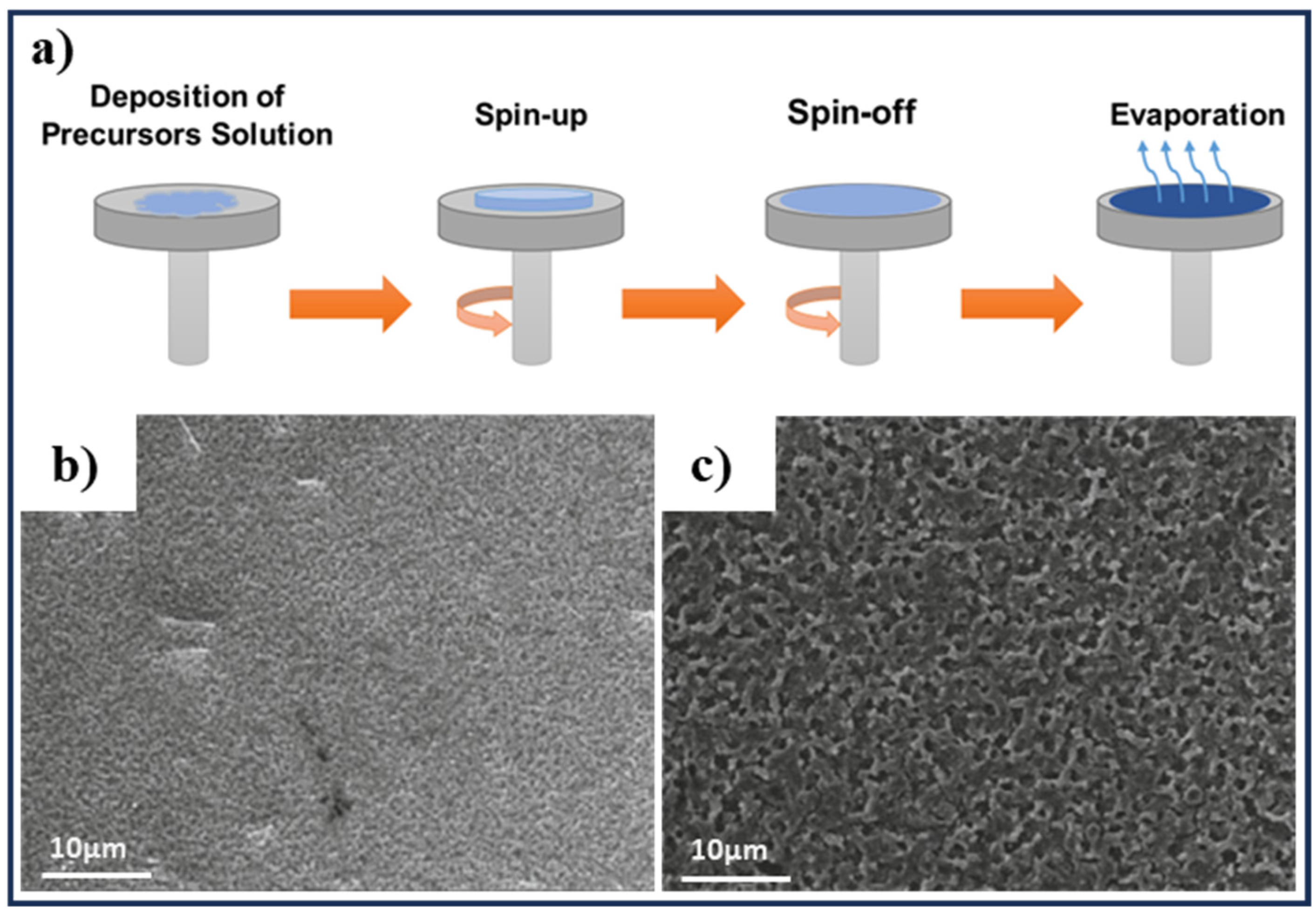
Spin coating is one of the most common methods to deposit a thin layer of polymers, nanoparticles, and biomaterials, which are in the solution form on a substrate. It consists of four main steps (Figure 13a), where small amounts of precursor solution are dropped on the substrate and centrifugal force results from spinning makes the solution flowing outward on the substrate. The rotational speed (rpm) and time are two important factors in this method which affect the thickness and characteristics of the deposited layer [145]. Several research groups investigated the effect of different process factors on the thin film properties of CZTS thin films [104,118,121,122,146,147]. Ahmoum et al. deposited CZTS thin film by spin-coating method at 2500 rpm for 30 s to study the effect of the preheated environment on its microstructural and optoelectronic properties. The fabricated thin films were preheated in various atmospheres (air, Ar, and N2) before sulfurization at 580 °C, and it was reported that using Ar and N2 atmospheres resulted in higher crystallinity, larger grain size, and homogenous surface morphology [118]. Majula et al. investigated the fabrication of CZTS thin films by spin-coating method in various compositions and crystallization degree, followed by annealing at 500 °C in an N2 atmosphere. They reported that non-stoichiometric precursors and low-spinning speeds resulted in a lower degree of crystallization and consequently, lower sheet resistance, and a high optical bandgap of ~1.66 eV. SEM images of non-stoichiometric and stoichiometric CZTS films deposited at a 3200 rpm spinning speed depicted in Figure 13b,c show a smoother and comparatively higher dense surface with smaller grains (<1 μm) and lower crystallization for nonstoichiometric films than stoichiometric films [119]. Agawane et al. studied the effect of annealing temperature in the range of 525 °C and 575 °C (under H2S gas atmosphere) on the morphological, structural, and optical properties of CZTS thin films, synthesized by sol–gel and spin-coating technique. CZTS films annealed at 575 °C exhibited an efficiency of 3.01% [120]. In the same direction, Ozdal et al. conducted a sol–gel spin-coating method to investigate the effect of annealing temperature on the crystallinity, morphology, and optical properties of CZTS thin films. The bandgap of the annealed films at 300 °C, 500 °C, and 550 °C was reported to be 1.58 eV against 1.63 eV for 400 °C which is responsible for poor optical performance [121].
Gupta et al. investigated the structural, morphological, and optical properties, and chemical bonding states of CZTS thin films synthesized by sol–gel spin-coated method, and doped by Cd and Mg [104]. Ziti et al. synthesized CZTS thin film by sol–gel spin-coating technique on ordinary glass substrates to study the effect of different annealing times on structural, compositional, morphological, optical, and electrical properties of CZTS thin films. It was revealed that the films deposited for 5 and 10 min annealing time exhibited different surface morphology close to the stoichiometry. The optical bandgap energy of CZTS films increased with the increasing annealing time, and was found to be 1.48 eV for 5 min annealing time [122].
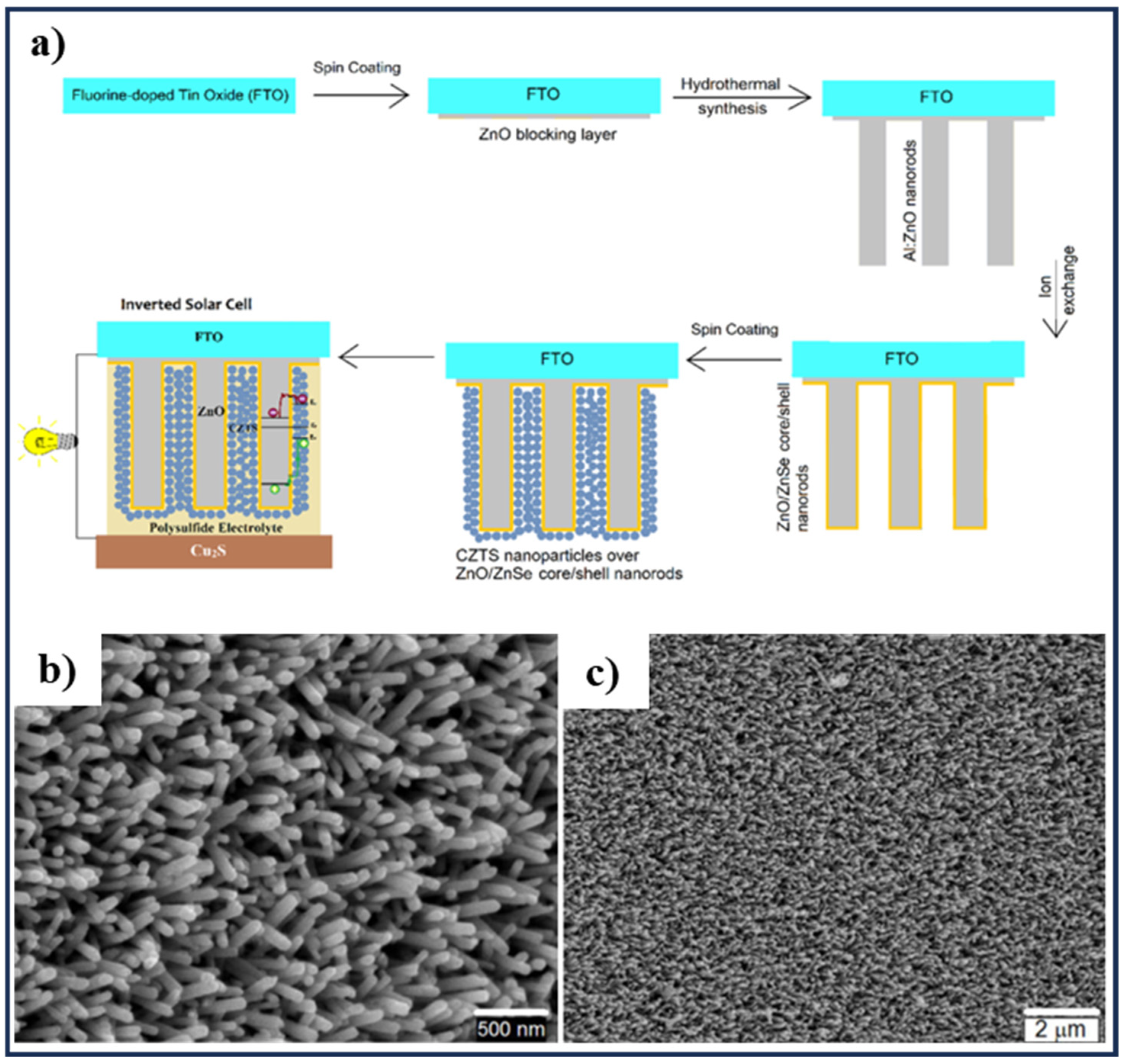
Akram et al. reported fabrication of ZnO/Al:ZnO/ZnS or ZnSe/CZTS core/shell vertically aligned nanorod arrays for liquid junction nanowire solar cells. The vertically aligned Al-doped zinc oxide nanorods (VANR) were developed on a ZnO seed layer deposited on fluorine-doped tin oxide (FTO) substrates. The surface of ZnO nanorods were transformed into ZnS or ZnSe, by an anion exchange process induced by the difference in solubility constant (Ksp) in a S2- or Se2- solution. It led to the formation of ZnO/ZnS and ZnO/ZnSe core-shell (CS) structures. In a separate process, CZTS nanoparticles were synthesized using high-temperature arrested precipitation and were later utilized to sensitize the ZnO/ZnS CS-VANR nanostructures. The steps in the process are shown in Figure 14a. From a high-magnification FE-SEM image (Figure 14b), the as-grown Al:ZnO nanorods appear aligned almost vertically to the substrate surface. The nanorods have an average diameter of 75 nm, and the aspect ratio is in the range of 15–25. It is observed that the integrity of the VANR array was not affected by Na2S treatment seen from the large-area top view of the sample (Figure 14c) [123].
This method provides a uniform thin film in the range of micrometer to nanometer on flat substrates by spreading precursor solution [145]. Despite the outstanding merits of the spin-coating method, some disadvantages come with it such as limitation in size and low material efficiency. Large size substrates cannot be coated using this method; furthermore, only 2–5% of the precursor solution which dropped on the substrate will be used, and another 95–98% of that will flung off in to the coating bowl and be disposed of [148].

3.2. Spray Pyrolysis Method

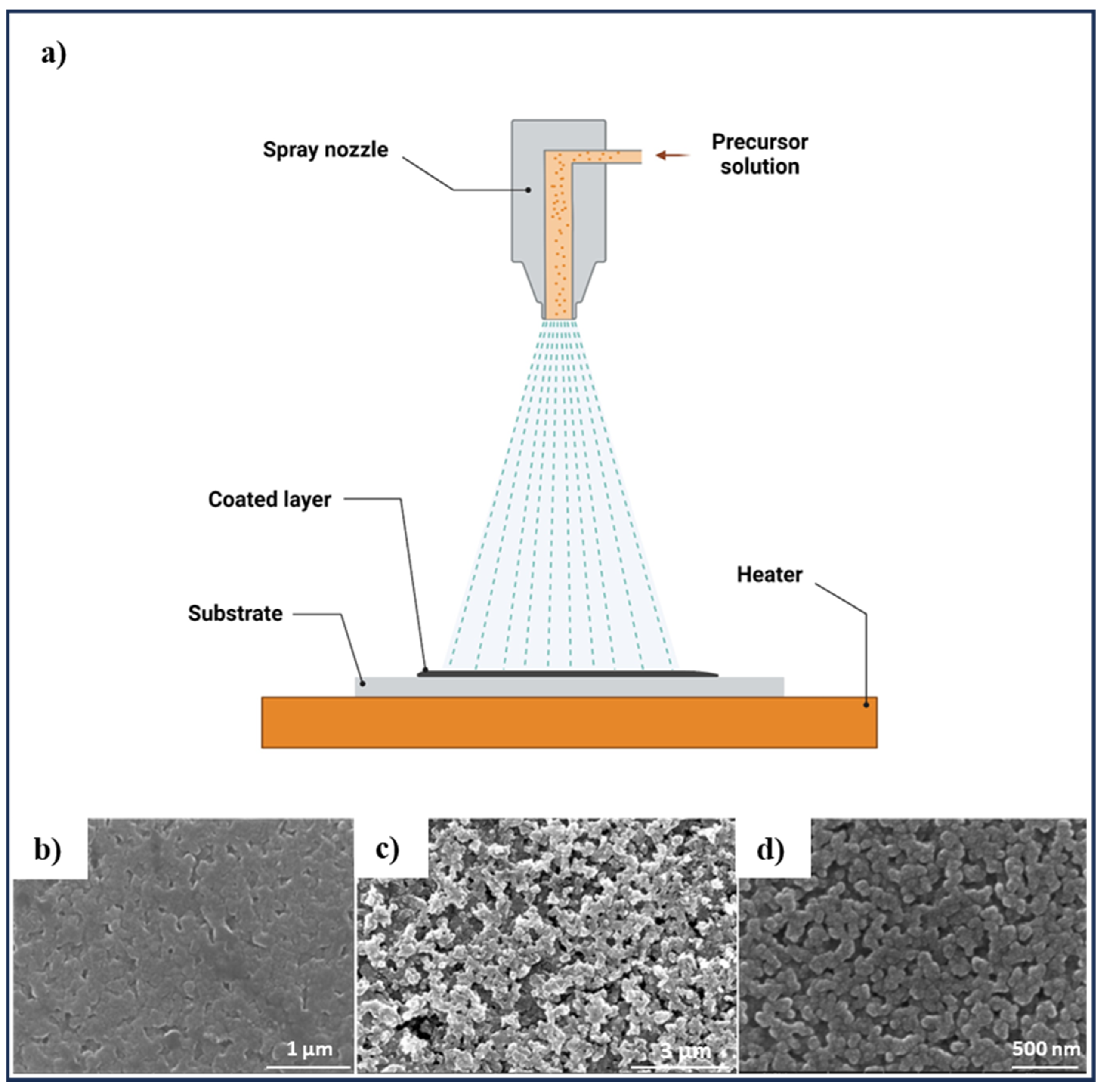
Spray pyrolysis is a chemical treatment method employed to generate ceramic coatings, thin and thick films, and powders and was performed for the first time in 1966 by Chamberlin and Skarman [6]. It is a non-vacuum, simple, and cost-effective technique, and has the ability to produce a large area of thin films which is desirable at an industrial scale [127,149]. A schematic of this method is shown in Figure 15a, whereby precursor solution is atomized in droplets and sprayed by nozzle toward substrate where chemical reactions take place in a vapor phase at moderately high temperature and the desired compound is generated [150]. Various spray pyrolysis techniques have been used to develop high-quality CZTS thin films with a good performance by studying a range of parameters. Nakayama and Ito were the first to use spray pyrolysis for the synthesis of stannite-phased CZTS films [151]. Critical parameters of spray pyrolysis, such as flow rate, carrier gas, substrate temperature, atmosphere, distance between nozzle and substrate, and precursor composition, significantly affect the characteristics of the produced film. Pyrolysis methods often use atomizers for spraying via ultrasonic, electrostatic, or air [6]. Kumar et al. reported the fabrication of single-phase CZTS without annealing and post-deposition sulfurization to study the effect of substrate temperature on the growth of CZTS films [125]. Kamoun et al. investigated the synthesis conditions and properties of CZTS thin films fabricated through spraying aqueous solutions of copper chloride, zinc chloride, tin chloride, and thiourea on heated glass substrates at various temperatures, and reported high crystallinity for 60 min of spraying on substrate at 613 K temperature [126]. Jeganath et al. examined the structural inhomogeneity of CZTS thin film fabricated by spray pyrolysis, and revealed the phase segregation to be the reason for surface inhomogeneity [127]. Khushaim et al. studied the effect of the substrate temperature (250, 300, and 350 °C) on the structural, morphological, and optical properties of the CZTS thin films fabricated by using the sol–gel method and the spray deposition technique. SEM images showed variation in the surface morphologies of CZTS films obtained with varying substrate temperature (Figure 15b–d). CZTS films at 250 °C substrate temperature exhibited agglomerations of small grains with some voids in between (Figure 15b) to a dense surface associated with the porous structure and significantly clear grains (Figure 15c) for 300 °C, and the presence of separate grains that tend to grow by coalescing together (Figure 15d) for 350 °C. Moreover, it was reported that the films deposited on a substrate with low temperature revealed a high bandgap value (∼1.8 eV) and it decreased to 1.6 eV with increasing the substrate temperature to 300 °C due to improved microstructure [79].
The spray pyrolysis technique offers several benefits, including a straightforward equipment setup, a simple and cost-effective experimental procedure, a high-deposition rate, and the production of layers with uniform composition. The surface morphology and thickness of the layer can be adjusted by the deposition temperature and the size of the atomized droplets. Nevertheless, a significant drawback of this method is the loss of precursors during spraying. Scaling up or achieving uniform layers over large areas poses challenges. Additionally, there is a risk of sulfides oxidizing during the deposition process in an air atmosphere [3,149].

3.3. Thermal Evaporation

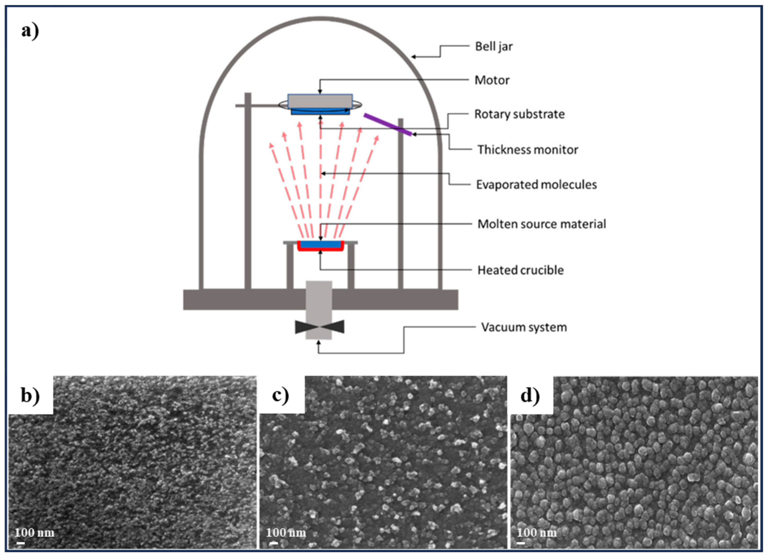
In this method, which enables nanoscale thickness coatings, the source material is heated to a high temperature within a vacuum, causing it to evaporate and vapors directly reach a low-temperature substrate where they solidify and form a thin layer [56,152]. In this method, resistive heating is commonly used for thin film deposition, and the source materials are in the form of powder or solid bar, evaporated by a heated filament or boat [153]. Since the target and the substrate have a significant temperature difference, a temperature gradient forms which leads to a vapor stream that flows from the target to the surface of substrates. As the atoms or molecules hit the surface, they condense back into a solid state (Figure 16a) [56]. Since resistive heating cannot melt materials having a high-melting point, another form of physical vapor deposition method, i.e., electron beam deposition, is used [153]. Sripan et al. studied the effect of sulfurization and annealing on various phase changes and on the light-harvesting capability of CZTS absorber layers fabricated by the thermal evaporation method on substrate when using single-source materials which was synthesized by molten technique [128]. It was reported that as-deposited CZTS film contains a Sn2S3 secondary phase, while for the films annealed at 450 °C and 500 °C, and sulfurized at 550 °C, no unwanted secondary phases were detected [128]. CZTS films were grown using a thermal evaporation technique onto non-heated substrates by Khemiri et al. to study the effect of different annealing atmosphere, i.e., (a) vacuum annealing atmosphere, and (b) sulfur annealing atmosphere followed by vacuum annealing on the properties of CZTS film [129]. Figure 16b–d revealed a different surface morphology of the CZTS thin film where the deposited sample (Figure 16b) exhibited a flat and smooth surface morphology with negligible grains, due to the amorphous nature of the film. After annealing, the surface morphology changed to a non-uniform surface with sparsely distributed grains, whereas the sample annealed under sulfur atmosphere followed by vacuum annealing exhibited a homogeneous and compact surface with densely packed grains. The most adequate properties fulfilling the requirements of the absorber layer were reported for the second annealing condition [129]. In another study, CZTS thin film was obtained by thermal evaporation method using pure phase CZTS nano-structured bulk material, prepared using a solution method with water, ethylene glycol, and ethylenediamine as solvents. The formation of polycrystalline CZTS thin film with a tetragonal crystal structure after annealing at 450 °C having a direct bandgap of ~1.36 eV was reported [130].

3.4. Electron Beam Evaporation

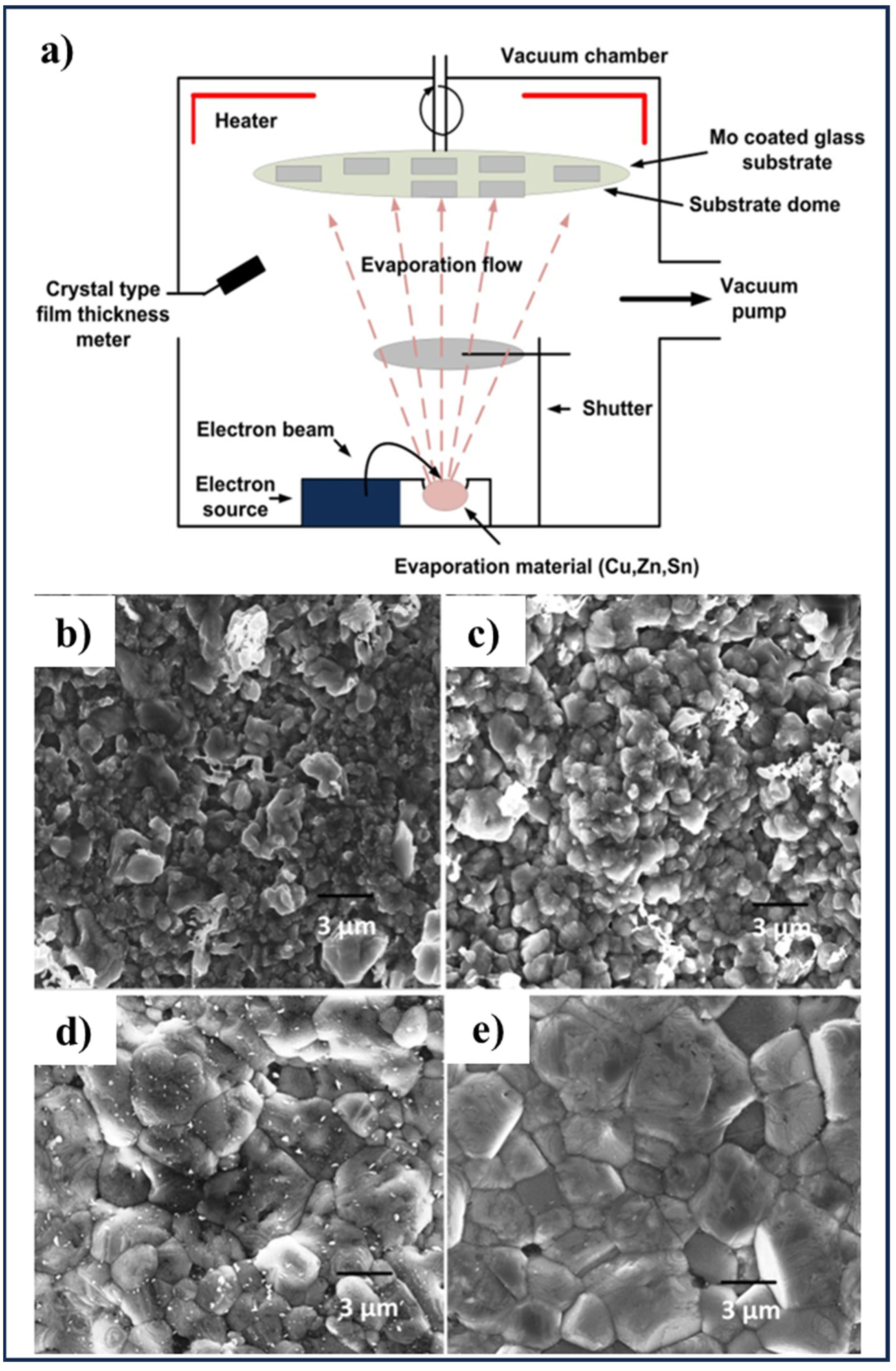
In electron beam evaporation, an electron beam is used to heat the target resulting in the evaporation of materials in the form of vapors, which then condense on substrates in high-vacuum conditions [154]. Heated filament causes the thermionic emission of electrons, which then accelerates under a potential difference towards the target material, thus providing sufficient energy for evaporation. A schematic of the electron beam evaporation process is shown in Figure 17a. The filament is located out of sight of the evaporant to avoid melting of the filament and the electron beam is pulled around to the surface by a magnetic field [152]. Tiwari et al. reported fabrication of CZTSe thin films through the electron beam eavporation method with different electron beam currents (between few mA to 110 mA), and by using pre-synthesized bulk source near stoichiometric CZTSe via the solid-state synthesis method [131]. The deposition of a sandwich device of Al/CZTS/Al thin films was reported by Azim-Araghi et al. by electron beam gun evaporation method from CZTS powder synthesized using a microwave-assisted technique. CZTS powders were synthesized using Cu(NO3)2·3H2O, Zn(NO3)·6H2O, Sn(SO4)·6H2O, and Na2S·xH2O dissolved in ethylene glycol (EG) on a magnetic stirrer at room temperature. Sandwich devices (Al (50 nm)/CZTS (80 nm)/Al (50 nm)) were deposited with a depositing rate of 0.5 nm/S at room temperature on precleaned glass [132]. Mkawi et al. studied the effect of substrate temperature on the morphological, optical, and structural properties of CZTS thin films deposited by electron beam evaporation. In that study, CZTS thin films were fabricated by e-beam deposition of the CZT precursors on pre-heated substrates followed by a sulfurization step. The films were deposited on Mo-coated glass substrate with a deposition rate of ~10 nm s−1 at different substrate temperatures. The FE-SEM images of CZTS thin films grown at different substrate temperatures illustrated the surface morphology, which revealed a rough surface with pinholes of varying sizes for 220 °C (Figure 17b). The surface of the sample with substrate at 250 °C was uniform with fine grains forming large clusters with some voids as shown in Figure 17c. The substrate temperature of 280 °C revealed a nearly smooth surface and increased grain size (Figure 17d). The large size grains surrounded by smaller grains was found in the substrate deposited at 310 °C temperature (Figure 17e) [133].

3.5. Successive Ionic Layer Adsorption and Reaction (SILAR) Method

The successive ionic layer adsorption and reaction (SILAR) method uses a chemical approach for creating large, uniform thin films, and involves submerging the substrate into separate cation and anion solutions. Figure 18 shows the detailed schematic of the SILAR method. This technique has been effectively used for various materials like metal sulfides, selenides, tellurides, and oxides. SILAR stands out among other film deposition methods due to its low temperature requirement, use of aqueous solutions, layer-by-layer growth, and distinct sources for anions and cations. The SILAR method was first used by Mali et al. to deposit CZTS thin films onto the FTO substrates. CuSO4, ZnSO4, and SnSO4 solutions were dissolved in H2O giving Cu2+, Zn2+, Sn2+ anions, while Na2S was dissolved in H2O giving S2− cations, and the CZTS uniform thin film consisting of particles with an average grain size of 100 nm was achieved by the sequential immersion of substrate in cationic and anionic solutions. Rinsing in deionized water was applied after every immersion [134]. Krishnan et al. synthesized CZTS thin films using a single cationic bath by a modified SILAR route, with a separate bath for Zn2+ ions to avoid the formation of Cu3SnS4 (CTS) and Cu2S phases rather than phase pure CZTS, the process was followed by annealing at elevated temperature [135]. Murugan et al. prepared nano-crystalline CZTS thin films on the conducting and nonconducting substrates by SILAR method for different dipping times. The bandgap of the obtained films was reported in the range of 1.46–1.82 eV [136]. Kumar et al. investigated the effect of Ar annealing on the physical properties of CZTS thin films, deposited by the SILAR process in various precursor concentrations, dipping times, and numbers of cycles. It was reported that the surface of the as-deposited film contains a few voids and cracks which were decreased by annealing films at 250 °C for 1 h, in an Ar atmosphere, resulting in achieving a thin film with higher density [137].

3.6. Pulsed Laser Deposition

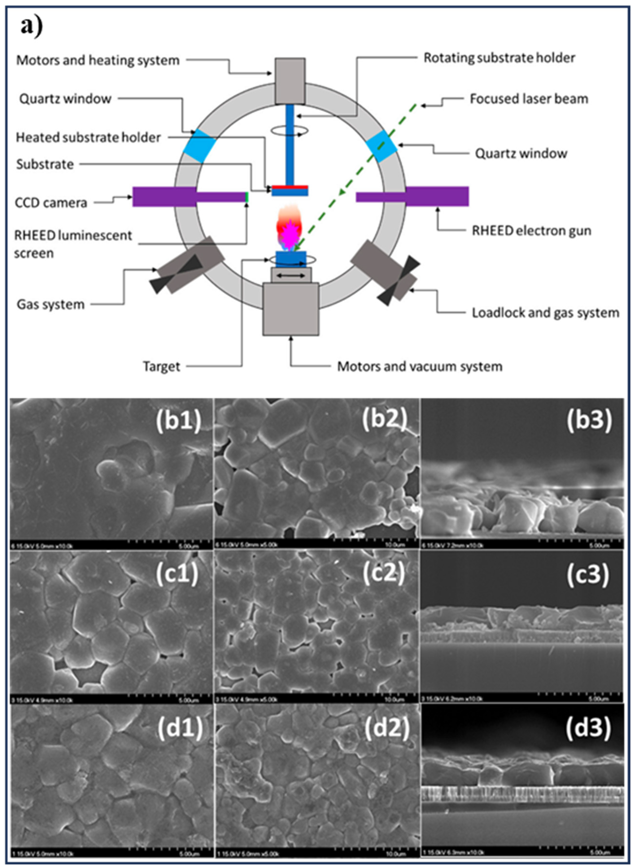
A simple and versatile vacuum-based technique which is used for thin film deposition of a wide range of alloys or compounds with a sensitive chemical composition onto a variety of substrates is pulsed laser deposition (PLD). In this method, which is a modifyed thermal evaporation process, a high-power pulsed laser is irradiated onto the target of charged materials through a quartz window which evaporates atoms from the target surface and these atoms are further collected on substrates to form thin films (Figure 19a) [56,153]. The first step of the PLD process for producing CZTS thin films is the formation of the CZTS target which is fabricated by other processes such as mechanochemical or solid-state reaction. In the next step, the CZTS target is evaporated by a focused high-power pulsed laser beam inside a vacuum chamber which is deposited on a substrate as a thin film. The properties of the deposited film can be controlled by different parameters such as target material, target-to-substrate distance, pulse energy, pulse repetition rate, substrate temperature, substrate orientation, and type of gas and its pressure in the chamber. Usually, a subsequent annealing process is needed since deposited CZTS thin films are amorphous, and their crystallinity need to be be improved [155]. Vanalakar et al. studied the effect of annealing atmospheres such as Ar, N2, and S powder on the structural properties and surface morphologies of CZTS thin film deposited by the PLD process. The CZTS tablet as a target was synthesized by the mechanochemical processing of Cu2S, ZnS, and SnS2 powders mixed with a 1:1:1 molar ratio [138]. It was reported that the variation of the annealing atmosphere does not affect the crystal structure, while the grain size varies and it increases with S content atmosphere (Figure 19b–d), resulting in a significant increase in the structural, optical, surface morphological, and electrical properties of CZTS thin films [138]. Wibowo et al. reported the thin film deposition of the CZTSSe quaternary compound by PLD method on substrates with various temperatures ranging from room temperature to 500 °C. Ball milling and uniaxial pressing were conducted to prepare the CZTSSe target from CuSe2, ZnSe, Sn, and Se powders [139]. Lee et al. used the PLD method for the deposition of modified CZTSSe thin films with Pb and Ti (a small amount of Pb and Ti was added to the CZTSe target) [140].
The PLD technique provides unique advantages such as a high-deposition rate, effortless species transfer from target to substrate, growth from energetic beam, and reactive deposition [56]. Also, by varying the deposition parameters, the PLD technique can create films of desired thickness, morphology, and composition, as well as deposit different target materials with unique properties on a single substrate [156]. The evaporation using laser ablation does not rely on the vapor pressures which results in controlled film composition. Laser ablation in the PLD process generates particulates of micrometer size. Moreover, a narrow plasma distribution from the laser ablation process cannot cover a large area and poses difficulty for large area thin film preparation [3].

3.7. Electrochemical Deposition Method

Electrodeposition is a highly promising method for the low-cost manufacturing of thin film absorber layers’ fabrication. The equipment required for this method is inexpensive, and the process is energy efficient, typically operating near room temperature. Electrodeposition offers excellent control over film characteristics such as grain size, crystallinity, and composition. Its ability to provide conformal coverage makes it ideal for mass production and is particularly well suited for applications in the large-area thin film deposition [157]. This deposition method requires an electrochemical cell setup including electrolyte with the desired ions, a cathode (substrate) and an anode, and applying voltage to induce the reduction of metal ions at the cathode. The process involves applying an electric field and redox reactions to deposit conducting or semiconducting materials onto a substrate [158].
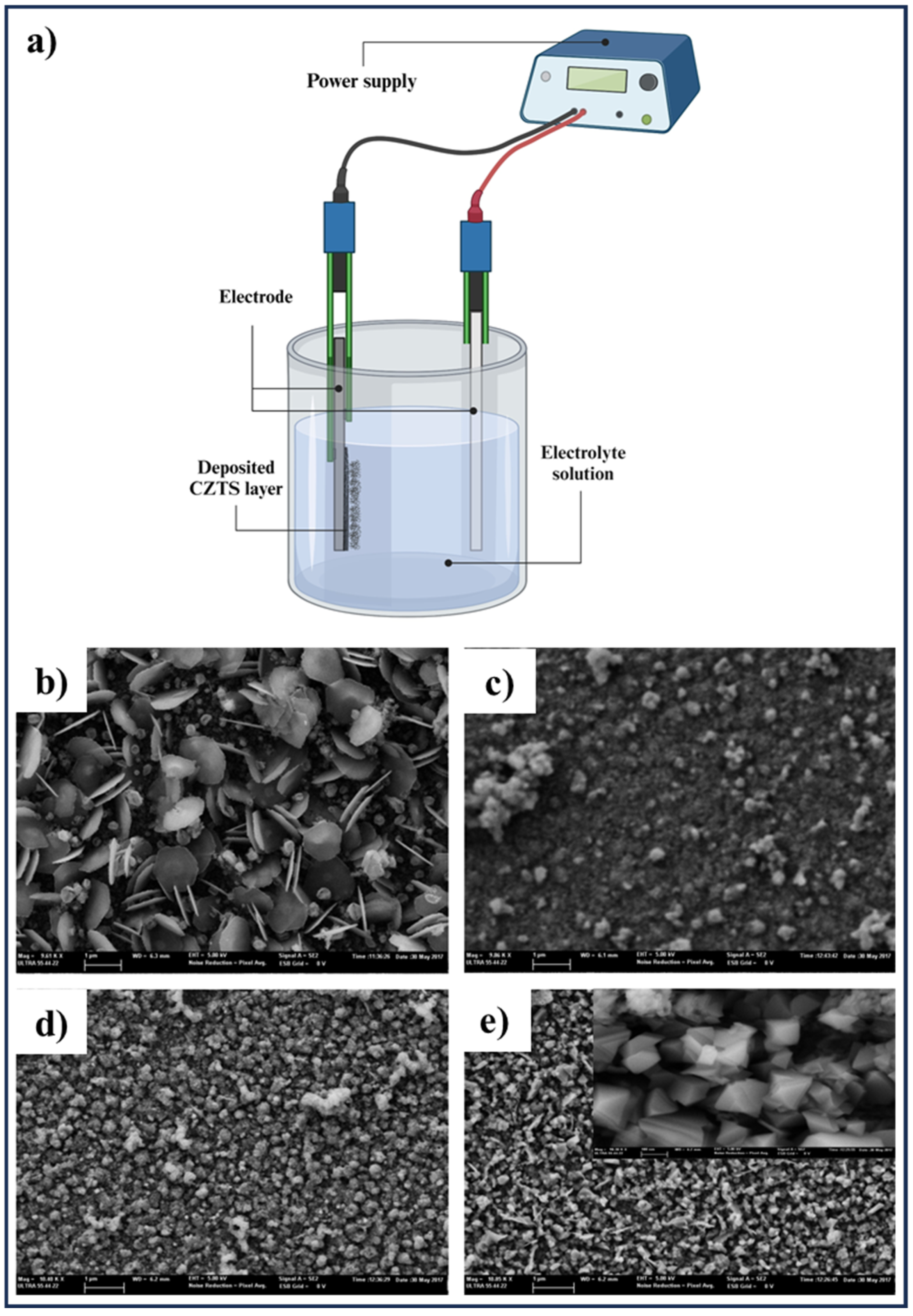
Through this technique, the configuration, morphology, and dimensions of electrocatalysts can be controlled on the surface of conductive materials by adjusting the parameters of electrochemical deposition. Furthermore, in the electrochemical deposition method, there is no capping reagent or surfactant or other dispersion agent involved [159]. In this approach, for the deposition process to occur, the substrate must be in electrical contact while submerged in a liquid bath, and it must be coated with a material capable of conducting electricity on its surface beforehand. A schematic diagram of a typical setup for electroplating is shown in the Figure 20a. The deposition of CZTS thin films by the electrochemical route appears to be of great interest due to its easy fabrication procedure, non-vacuum and low-cost technology, use of non-toxic solvents and reagents, with high throughput and high-material utilization along with room temperature operability. Additionally, electrodeposition is a well-established industrial technique for depositing semiconductors over large areas, ensuring superior uniformity in composition [141]. Importantly, electrochemically deposited thin films are largely nanostructured. Inguanta et al. deposited CZTS thin film by one-step potentiostatic deposition under N2 atmosphere from a de-aerated aqueous solution involving CuSO4, ZnSO4, SnSO, and Na2S2O3 on ITO/PTE substrates at room temperature [141]. Ziti et al. fabricated CZTS thin film on ITO glass substrates by using a one-step electrodeposition method to study the effect of sulfurization in an N2 + H2S atmosphere at different temperatures (350 °C, 375 °C, 400 °C, and 425 °C) for 10 min on structural, morphological, and optical properties of films. SEM images (Figure 20b–e) revealed the effect of the sulfurization temperatures on the growth process of the Cu2ZnSnSe4 film. At low temperatures, the substrate is not fully covered by the material, and the unstable cluster morphology indicates that the temperature is too low for grain formation and crystallization of the CZTS phase. As the temperature increases, nucleation improves, and coalescence begins. During this process, the clusters come together through cluster–cluster interactions, shaping the particles and resulting in small, semi-granular particles. The process culminates in the crystallization of CZTS films, where particles take on a tetragonal shape [142]. Chen et al. reported electrodeposition of CZTS films by using Reline as a green electrolyte. Fabrication of thin film CZTS was conducted by co-electrodepositing Cu–Zn–Sn precursor thin films in Reline subjected to sulfurization at 550 °C for 1 h [143]. Urazov et al. used one-step electrodeposition method to deposite Cu2ZnSnSe4 thin film onto polyaniline/FTO/glass substrate to study the CZTSe nucleation in the course of the film formation. The SEM results showed the nanocrystals with a size of 25–50 nm in the deposited CZTSe film [144]. Li et al. reported the formation of high-crystalline quality Cu2ZnSnSe4 thin film by co-electrodeposition method followed by heat treatment in a element selenium atmosphere [160].
Selecting a thin film deposition method for CZTS fabrication is often driven by the specific requirements of the product, balancing factors such as film quality and characteristics, substrate compatibility, environmental considerations, and cost efficiency. In this review, we have discussed the different methods for CZTS thin film deposition, each with its unique advantages and limitations that are tailored to specific applications. Spin coating and SILAR are highly favored for research and development applications of CZTS compounds due to their simplicity and cost effectiveness. Spray pyrolysis and electrochemical deposition are scalable, making them suitable for industrial applications. Spray pyrolysis is adept at covering large substrate areas and is often used in the production of large-scale solar panels. Thermal evaporation, electron beam evaporation, and PLD are preferred when high purity and precise control over film properties are crucial. Thermal and electron beam evaporation are particularly useful where high-purity CZTS is required. The choice of deposition method depends on the required film quality, desired properties, substrate characteristics, environmental impacts, and economic considerations.

4. Addressing Hurdles in Using CZTS/Se Nanomaterials towards Improving Thin Film Solar Cell Performance

While substantial endeavors have been directed towards the synthesis of CZTS/Se materials at the nanoscale and their subsequent transformation into thin film structures, achieving optimally tuned properties for efficient operation across diverse applications remains a significant challenge. Given a predominant focus on second generation thin film PV devices, extensive research efforts have been undertaken to enhance their performace under 1 sun illumination. CZTS/Se exhibits comparatively more resistance to heat than Si solar cells, and contains non-toxic and harmful components. However, achieving improved performance of solar cells takes longer and is comparatively less efficient than conventional solar cells. Notwithstanding the notable attributes of CZTS/Se nanoscale absorbers, the ongoing pursuit of improvement with the low-cost methodology remains a fundamental challenge within the research community.
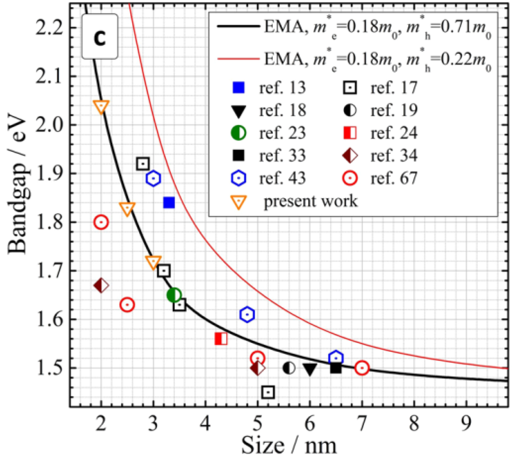
CZTS-based solar cells exhibit poor PV performace relative to CIGS thin dilm solar cells [161]. The enhancement of CZTS/Se efficiency towards 22.6% is observed through modified nanomaterials. The reason behind a lower PCE of CZTS/Se solar cells is the short minority carrier lifetimes, cation disorder, and recombination reactions resulting in the loss of charge carriers and hence lower open-circuit voltage (Voc). One of significant contributions to improved CZTS/Se solar cells is to reduce the recombination reactions and improving optical properties of CZTZ/Se nnaomaterials. It could be carried out by either varying the composition of the elements in CZTS/Se, synthesis conditions such as reaction temperature, choice of precusrsors, reation time, and method of synthesis. Along with this, thin film deposition conditions significantly matter, their structural and electrical properties varies with thickness and deposition rate, choice of solvents, and hence, can impact their PV performance [162,163,164]. Hence, the optimal CZTS precursors and synthesis process are the key to obtain the desired absorber layers, with modified CZTS structure and morphology, and particle size as they play a significant role in modulating their light absorption and surface energy [3,165]. Particle size of CZTS could control the optoelectronics properties, for example, CZTS nanoparticles induce spatial exciton confinement, leading to an enhanced absorption band edge position, and thus resulting in modified optical properties. It has been reported that the absorption of CZTS nanocrystals shows a size-dependent trend on the optical energy bandgap for sizes smaller than 4–5 nm. Figure 21 shows the experimental data of the size dependence of Eg for CZTS NCs (as scatter plots) and two calibration curves produced by using an effective hole mass (m*h) of 0.71m0 (the transverse contribution) and 0.18 m0 (the longitudinal contribution), where m0 is the electron rest mass. It has been demonstrated that the bandgap of CZTS NCs with an average size of 3 nm and 2 nm is 1.72 eV and 2.04 eV, respectively [166].
The formation of secondary phases during the synthesis of CZTS/Se is another challenge in the current research. The narrow phase stability in the pseudoternary phase diagram of CZTS, indicates the formation of defects and a secondary phase such as ZnS, CuxS, SnSx, or Cu2SnS3 during the growth and post-growth processes. It led to the structural inhomogeneity and presence of pin holes, which in turn results in the scattering within the absorber layers, hence leading to local fluctuations in VOC, high-carrier recombination, and low PCE of CZTS/Se solar cells. Numerous strategies have been demostrated so far to reduce the formation of secondary phases and defects during the process, such as defect passivation which is a process of mitigating defects including vacancies, interstitial atoms, impurities, grain boundaries, and other structural irregularities using post-surface modifications or doping, controlled stoichiometry in the post-annealing stage, and interfacial engineering at the CZTS/molybdenum interface [58]. Another approach is etching, and it has been widely used to remove secondary phases from absorber surfaces where an etchant is used to convert Cu-, Zn-, or Sn-related binary or ternary phases from the CZTS/Se absorber layer into water-soluble salt without affecting their composition. Considering the selective removal of secondary phases will significantly increase the short-circuit current density (JSC), reduce the series resistance (RS) of the CZTS device, and hence, improve the device performance [167,168,169].

5. Summary

The present review outlines the significance of CZTS nanomaterial synthesis techniques, shedding light on recent advancements and challenges, particularly in the context of solar energy harvesting, thus providing a comprehensive understanding essential for further advancements in the field. While CZTS/Se offers a sustainable solution for thin film PV, the cell performance is hampered by secondary phase formation. Addressing these challenges necessitates a multifaceted approach encompassing compositional variations, synthesis conditions, and thin film deposition parameters for improved light absorption and charge carrier dynamics in CZTS/Se thin films. Therefore, ongoing research efforts continue to explore novel methodologies and materials modifications aimed at advancing nanoscale CZTS/Se, highlighting the enduring commitment of the scientific community. Moreover, considerations regarding stability, sustainability of deposition processes, cost effectiveness, and integration of CZTS/Se nanomaterials into existing PV devices are of great significance. These perspectives not only shed light on the promising role of CZTS/Se nanoscale materials in PV technology but also emphasize its wider significance for achieving energy equity and enhancing accessibility.

Author Contributions

Conceptualization, D.R.R.; writing—original draft preparation, S.M.; writing—review and editing, S.M., N.K., and D.R.R., supervision, D.R.R.; project administration, D.R.R.; funding acquisition, D.R.R. All authors have read and agreed to the published version of the manuscript.

Funding

This work was funded in part by NASA, grant number 80NSSC10M020, and the US Department of Defense (DoD) Office of Naval Research (ONR), award N00014-20-1-2539, and NSF 2122078.

Acknowledgments

The authors acknowledge the funding from NASA, US DoD ONR, and US National Science Foundation.

Conflicts of Interest

The authors declare no conflicts of interest.

References

  1. Najm, A.S.; Al-Ghamdi, A.; Amin, M.T.; Al Ghamdi, A.; Moria, H.; Holi, A.M.; Abed, A.M.; Al-Zahrani, A.A.; Sopian, K.; Bais, B.; et al. Towards a promising systematic approach to the synthesis of CZTS solar cells. Sci. Rep. 2023, 13, 15418. [Google Scholar] [CrossRef] [PubMed]
  2. Olgar, M.A.; Erkan, S.; Zan, R. Dependence of CZTS thin film properties and photovoltaic performance on heating rate and sulfurization time. J. Alloys Compd. 2023, 963, 171283. [Google Scholar] [CrossRef]
  3. Amrillah, T. Enhancing the value of environment-friendly CZTS compound for next generation photovoltaic device: A review. Sol. Energy 2023, 263, 111982. [Google Scholar] [CrossRef]
  4. Patil, S.S.; Nadaf, S.N.; Mali, S.S.; Hong, C.K.; Bhosale, P.N. Optoelectronic and Photovoltaic Properties of the Cu2ZnSnS4 Photocathode by a Temperature-Dependent Facile Hydrothermal Route. Ind. Eng. Chem. Res. 2021, 60, 7816–7825. [Google Scholar] [CrossRef]
  5. Islam, M.F.; Md Yatim, N.; Hashim@Ismail, M.A. A Review of CZTS Thin Film Solar Cell Technology. J. Adv. Res. Fluid Mech. Therm. Sci. 2021, 81, 73–87. [Google Scholar] [CrossRef]
  6. Chtouki, T.; Hachimi, M.A.; Tarbi, A.; Erguig, H. Development of different characterizations of sprayed Cu2ZnSnS4 thin films: A review. Opt. Quantum Electron. 2023, 55, 342. [Google Scholar] [CrossRef]
  7. Shah, N.; Shah, A.A.; Leung, P.K.; Khan, S.; Sun, K.; Zhu, X.; Liao, Q. A Review of Third Generation Solar Cells. Processes 2023, 11, 1852. [Google Scholar] [CrossRef]
  8. ElKhamisy, K.; Abdelhamid, H.; El-Rabaie, E.-S.M.; Abdel-Salam, N. A Comprehensive Survey of Silicon Thin-film Solar Cell: Challenges and Novel Trends. Plasmonics 2024, 19, 1–20. [Google Scholar] [CrossRef]
  9. Di Sabatino, M.; Hendawi, R.; Garcia, A.S. Silicon Solar Cells: Trends, Manufacturing Challenges, and AI Perspectives. Crystals 2024, 14, 167. [Google Scholar] [CrossRef]
  10. Green, M.A. Silicon solar cells step up. Nat. Energy 2023, 8, 783–784. [Google Scholar] [CrossRef]
  11. Theelen, M.; Daume, F. Stability of Cu(In,Ga)Se2 solar cells: A literature review. Sol. Energy 2016, 133, 586–627. [Google Scholar] [CrossRef]
  12. Contreras, M.A.; Mansfield, L.M.; Egaas, B.; Li, J.; Romero, M.; Noufi, R.; Rudiger-Voigt, E.; Mannstadt, W. Wide bandgap Cu(In,Ga)Se2 solar cells with improved energy conversion efficiency. Prog. Photovolt. Res. Appl. 2012, 20, 843–850. [Google Scholar] [CrossRef]
  13. Nishinaga, J.; Kamikawa, Y.; Sugaya, T.; Ishizuka, S. Comparison of polycrystalline and epitaxial Cu(In, Ga)Se2 solar cells with conversion efficiencies of more than 21%. Sol. Energy Mater. Sol. Cells 2024, 269, 112791. [Google Scholar] [CrossRef]
  14. Geisthardt, R.M.; Topič, M.; Sites, J.R. Status and Potential of CdTe Solar-Cell Efficiency. IEEE J. Photovolt. 2015, 5, 1217–1221. [Google Scholar] [CrossRef]
  15. Oni, A.M.; Mohsin, A.S.M.; Rahman, M.M.; Hossain Bhuian, M.B. A comprehensive evaluation of solar cell technologies, associated loss mechanisms, and efficiency enhancement strategies for photovoltaic cells. Energy Rep. 2024, 11, 3345–3366. [Google Scholar] [CrossRef]
  16. Hossain, A.; Bandyopadhyay, P.; Karmakar, A.; Ullah, A.K.M.A.; Manavalan, R.K.; Sakthipandi, K.; Alhokbany, N.; Alshehri, S.M.; Ahmed, J. The hybrid halide perovskite: Synthesis strategies, fabrications, and modern applications. Ceram. Int. 2022, 48, 7325–7343. [Google Scholar] [CrossRef]
  17. Gupta, I.; Dey, A.; Jain, R. Non-toxic solution processed Cu2ZnSn(SSe)4 thin films for photovoltaic Applications: A review. Mater. Today Proc. 2023. [Google Scholar] [CrossRef]
  18. Khadir, A.; Lahoual, M.; Abdelhafidi, M.K.; Sengouga, N. Design of CZTS/CZTSe tandem solar cells with enhanced performance. Mater. Today Commun. 2023, 37, 107094. [Google Scholar] [CrossRef]
  19. Song, X.; Ji, X.; Li, M.; Lin, W.; Luo, X.; Zhang, H. A Review on Development Prospect of CZTS Based Thin Film Solar Cells. Int. J. Photoenergy 2014, 2014, 613173. [Google Scholar] [CrossRef]
  20. Suryawanshi, M.P.; Agawane, G.L.; Bhosale, S.M.; Shin, S.W.; Patil, P.S.; Kim, J.H.; Moholkar, A.V. CZTS based thin film solar cells: A status review. Mater. Technol. 2013, 28, 98–109. [Google Scholar] [CrossRef]
  21. Yussuf, S.T.; Nwambaekwe, K.C.; Ramoroka, M.E.; Iwuoha, E.I. Photovoltaic efficiencies of microwave and Cu2ZnSnS4 (CZTS) superstrate solar cells. Mater. Today Sustain. 2023, 21, 100287. [Google Scholar] [CrossRef]
  22. Rossetti, R.; Nakahara, S.; Brus, L.E. Quantum size effects in the redox potentials, resonance Raman spectra, and electronic spectra of CdS crystallites in aqueous solution. J. Chem. Phys. 1983, 79, 1086–1088. [Google Scholar] [CrossRef]
  23. Ikram, A.; Zulfequar, M.; Satsangi, V.R. Role and prospects of green quantum dots in photoelectrochemical hydrogen generation: A review. Int. J. Hydrog. Energy 2022, 47, 11472–11491. [Google Scholar] [CrossRef]
  24. Ikram, A.; Zulfequar, M. Visible light driven CZTS QDs/α-Fe2O3-graphene p–n heterojunction for photoelectrochemical water splitting. Nanotechnology 2023, 34, 315403. [Google Scholar] [CrossRef] [PubMed]
  25. Sahai, S.; Ikram, A.; Rai, S.; Shrivastav, R.; Dass, S.; Satsangi, V.R. Quantum dots sensitization for photoelectrochemical generation of hydrogen: A review. Renew. Sustain. Energy Rev. 2017, 68, 19–27. [Google Scholar] [CrossRef]
  26. Yu, K.; Chen, J. Enhancing Solar Cell Efficiencies through 1-D Nanostructures. Nanoscale Res. Lett. 2008, 4, 1. [Google Scholar] [CrossRef]
  27. Isotta, E.; Pugno, N.M.; Scardi, P. Nanostructured kesterite (Cu2ZnSnS4) for applications in thermoelectric devices. Powder Diffr. 2019, 34, S42–S47. [Google Scholar] [CrossRef]
  28. Kumar, S.; Ansari, M.Z.; Khare, N. Influence of compactness and formation of metallic secondary phase on the thermoelectric properties of Cu2ZnSnS4 thin films. Thin Solid Film. 2018, 645, 300–304. [Google Scholar] [CrossRef]
  29. Yang, H.; Jauregui, L.A.; Zhang, G.; Chen, Y.P.; Wu, Y. Nontoxic and abundant copper zinc tin sulfide nanocrystals for potential high-temperature thermoelectric energy harvesting. Nano Lett. 2012, 12, 540–545. [Google Scholar] [CrossRef]
  30. Long, B.D.; Van Khanh, N.; Binh, D.N.; Hai, N.H. Thermoelectric properties of quaternary chalcogenide Cu2ZnSnS4 synthesised by mechanical alloying. Powder Metall. 2020, 63, 220–226. [Google Scholar] [CrossRef]
  31. Gour, K.S.; Bhattacharyya, B.; Singh, O.P.; Yadav, A.K.; Husale, S.; Singh, V.N. Nanostructured Cu2ZnSnS4 (CZTS) thin film for self-powered broadband photodetection. J. Alloys Compd. 2018, 735, 285–290. [Google Scholar] [CrossRef]
  32. Yu, X.; Shavel, A.; An, X.; Luo, Z.; Ibáñez, M.; Cabot, A. Cu2ZnSnS4-Pt and Cu2ZnSnS4-Au Heterostructured Nanoparticles for Photocatalytic Water Splitting and Pollutant Degradation. J. Am. Chem. Soc. 2014, 136, 9236–9239. [Google Scholar] [CrossRef]
  33. Chang, Z.-X.; Chong, R.-F.; Meng, Y.-N.; Zhou, W.-H.; Kou, D.-X.; Zhou, Z.-J.; Wu, S.-X. High temperature recrystallization of kersterite Cu2ZnSnS4 towards enhanced photocatalytic H2 evolution. Int. J. Hydrog. Energy 2015, 40, 13456–13462. [Google Scholar] [CrossRef]
  34. Gogoi, G.; Arora, S.; Vinothkumar, N.; De, M.; Qureshi, M. Quaternary semiconductor Cu2ZnSnS4 loaded with MoS2 as a co-catalyst for enhanced photo-catalytic activity. RSC Adv. 2015, 5, 40475–40483. [Google Scholar] [CrossRef]
  35. Zhou, X.; Gu, X.; Chen, Z.; Wu, Y.; Xu, W.; Bao, J. A novel and sensitive Cu2ZnSnS4 quantum dot–based non–enzymatic glucose sensor. Sens. Actuators B Chem. 2021, 329, 129117. [Google Scholar] [CrossRef]
  36. Gurav, K.V.; Shin, S.W.; Patil, U.M.; Deshmukh, P.R.; Suryawanshi, M.P.; Agawane, G.L.; Pawar, S.M.; Patil, P.S.; Lee, J.Y.; Lokhande, C.D.; et al. Cu2ZnSnS4 (CZTS)-based room temperature liquefied petroleum gas (LPG) sensor. Sens. Actuators B Chem. 2014, 190, 408–413. [Google Scholar] [CrossRef]
  37. Zhang, Y.; Zhou, S.; Sun, K. Cu2ZnSnS4 (CZTS) for Photoelectrochemical CO2 Reduction: Efficiency, Selectivity, and Stability. Nanomaterials 2023, 13, 2762. [Google Scholar] [CrossRef] [PubMed]
  38. Chen, Y.; Feng, X.; Liu, M.; Su, J.; Shen, S. Towards efficient solar-to-hydrogen conversion: Fundamentals and recent progress in copper-based chalcogenide photocathodes. Nanophotonics 2016, 5, 524–547. [Google Scholar] [CrossRef]
  39. Mahalakshmi, V.; Venugopal, D.; Ramachandran, K.; Ramesh, R. Synthesis of 2D-CZTS nanoplate as photocathode material for efficient PEC water splitting. J. Mater. Sci. Mater. Electron. 2022, 33, 8493–8503. [Google Scholar] [CrossRef]
  40. Wang, J.; Yu, N.; Zhang, Y.; Zhu, Y.; Fu, L.; Zhang, P.; Gao, L.; Wu, Y. Synthesis and performance of Cu2ZnSnS4 semiconductor as photocathode for solar water splitting. J. Alloys Compd. 2016, 688, 923–932. [Google Scholar] [CrossRef]
  41. Li, L.; Wang, C.; Feng, K.; Huang, D.; Wang, K.; Li, Y.; Jiang, F. Kesterite Cu2ZnSnS4 thin-film solar water-splitting photovoltaics for solar seawater desalination. Cell Rep. Phys. Sci. 2021, 2, 100468. [Google Scholar] [CrossRef]
  42. Shu, J.; Tang, D. Current Advances in Quantum-Dots-Based Photoelectrochemical Immunoassays. Chem. Asian. J. 2017, 12, 2780–2789. [Google Scholar] [CrossRef]
  43. Ceylan, S.; Küçükosman, R.; Yurt, F.; Özel, D.; Öztürk, İ.; Demir, D.; Ocakoglu, K. Antimicrobial activity enhancement of PVA/chitosan films with the additive of CZTS quantum dots. Polym. Bull. 2023, 80, 11273–11293. [Google Scholar] [CrossRef]
  44. Kumar, R.S.; Maddirevula, S.; Easwaran, M.; Dananjaya, S.H.S.; Kim, M.-D. Antibacterial activity of novel Cu2ZnSnS4 nanoparticles against pathogenic strains. RSC Adv. 2015, 5, 106400–106405. [Google Scholar] [CrossRef]
  45. Ocakoglu, K.; Dizge, N.; Colak, S.; Ozay, Y.; Bilici, Z.; Yalcin, M.S.; Özdemir, S.; Yatmaz, H. Polyethersulfone membranes modified with CZTS nanoparticles for protein and dye separation: Improvement of antifouling and self-cleaning performance. Colloids Surf. A Physicochem. Eng. Asp. 2021, 616, 126230. [Google Scholar] [CrossRef]
  46. Colak, S.; Vejselova Sezer, C.; Demirdogen, R.E.; Ince, M.; Emen, F.; Ocakoglu, K.; Kutlu, H.M. Investigation of in vitro Activities of Cu2ZnSnS4 Nanoparticles in Human Non-Small Cell Lung Cancer. Mater. Today Commun. 2021, 27, 102304. [Google Scholar] [CrossRef]
  47. Tang, T.; Xu, X.; Wang, Z.; Tian, J.; Yang, Y.; Ou, C.; Bao, H.; Liu, T. Cu2ZnSnS4 nanocrystals for microwave thermal and microwave dynamic combination tumor therapy. Chem. Commun. 2019, 55, 13148–13151. [Google Scholar] [CrossRef]
  48. Shi, Z.; Attygalle, D.; Jayatissa, A.H. Kesterite-based next generation high performance thin film solar cell: Current progress and future prospects. J. Mater. Sci. Mater. Electron. 2017, 28, 2290–2306. [Google Scholar] [CrossRef]
  49. Chen, S.; Gong, X.G.; Walsh, A.; Wei, S.-H. Crystal and electronic band structure of Cu2ZnSnX4 (X = S and Se) photovoltaic absorbers: First-principles insights. Appl. Phys. Lett. 2009, 94, 041903. [Google Scholar] [CrossRef]
  50. Khare, A.; Himmetoglu, B.; Johnson, M.; Norris, D.J.; Cococcioni, M.; Aydil, E.S. Calculation of the lattice dynamics and Raman spectra of copper zinc tin chalcogenides and comparison to experiments. J. Appl. Phys. 2012, 111, 083707. [Google Scholar] [CrossRef]
  51. Schorr, S.; Hoebler, H.-J.; Tovar, M. A neutron diffraction study of the stannite-kesterite solid solution series. Eur. J. Mineral. 2007, 19, 65–73. [Google Scholar] [CrossRef]
  52. Schorr, S. The crystal structure of kesterite type compounds: A neutron and X-ray diffraction study. Sol. Energy Mater. Sol. Cells 2011, 95, 1482–1488. [Google Scholar] [CrossRef]
  53. Shockley, W.; Queisser, H.J. Detailed Balance Limit of Efficiency of p-n Junction Solar Cells. J. Appl. Phys. 1961, 32, 510–519. [Google Scholar] [CrossRef]
  54. Li, Y.; Wei, H.; Cui, C.; Wang, X.; Shao, Z.; Pang, S.; Cui, G. CZTSSe solar cells: Insights into interface engineering. J. Mater. Chem. A 2023, 11, 4836–4849. [Google Scholar] [CrossRef]
  55. Boerasu, I.; Vasile, B.S. Current Status of the Open-Circuit Voltage of Kesterite CZTS Absorber Layers for Photovoltaic Applications-Part I, a Review. Materials 2022, 15, 8427. [Google Scholar] [CrossRef] [PubMed]
  56. Xie, H.; Sánchez, Y.; López-Marino, S.; Espíndola-Rodríguez, M.; Neuschitzer, M.; Sylla, D.; Fairbrother, A.; Izquierdo-Roca, V.; Pérez-Rodríguez, A.; Saucedo, E. Impact of Sn(S,Se) Secondary Phases in Cu2ZnSn(S,Se)4 Solar Cells: A Chemical Route for Their Selective Removal and Absorber Surface Passivation. ACS Appl. Mater. Interfaces 2014, 6, 12744–12751. [Google Scholar] [CrossRef] [PubMed]
  57. Kumar, M.; Dubey, A.; Adhikari, N.; Venkatesan, S.; Qiao, Q. Strategic review of secondary phases, defects and defect-complexes in kesterite CZTS–Se solar cells. Energy Environ. Sci. 2015, 8, 3134–3159. [Google Scholar] [CrossRef]
  58. Olekseyuk, I.D.; Dudchak, I.V.; Piskach, L.V. Phase equilibria in the Cu2S–ZnS–SnS2 system. J. Alloys Compd. 2004, 368, 135–143. [Google Scholar] [CrossRef]
  59. Dudchak, I.V.; Piskach, L.V. Phase equilibria in the Cu2SnSe3–SnSe2–ZnSe system. J. Alloys Compd. 2003, 351, 145–150. [Google Scholar] [CrossRef]
  60. Nagoya, A.; Asahi, R.; Wahl, R.; Kresse, G. Defect formation and phase stability of Cu2ZnSnS4 photovoltaic material. Phys. Rev. B 2010, 81, 113202. [Google Scholar] [CrossRef]
  61. Choubrac, L.; Lafond, A.; Guillot-Deudon, C.; Moëlo, Y.; Jobic, S. Structure Flexibility of the Cu2ZnSnS4 Absorber in Low-Cost Photovoltaic Cells: From the Stoichiometric to the Copper-Poor Compounds. Inorg. Chem. 2012, 51, 3346–3348. [Google Scholar] [CrossRef] [PubMed]
  62. Lund, E.A.; Du, H.; Hlaing Oo, W.M.; Teeter, G.; Scarpulla, M.A. Investigation of combinatorial coevaporated thin film Cu2ZnSnS4 (II): Beneficial cation arrangement in Cu-rich growth. J. Appl. Phys. 2014, 115, 173503. [Google Scholar] [CrossRef]
  63. Ibn-Mohammed, T.; Koh, S.C.L.; Reaney, I.M.; Acquaye, A.; Schileo, G.; Mustapha, K.B.; Greenough, R. Perovskite solar cells: An integrated hybrid lifecycle assessment and review in comparison with other photovoltaic technologies. Renew. Sustain. Energy Rev. 2017, 80, 1321–1344. [Google Scholar] [CrossRef]
  64. Maalouf, A.; Okoroafor, T.; Jehl, Z.; Babu, V.; Resalati, S. A comprehensive review on life cycle assessment of commercial and emerging thin-film solar cell systems. Renew. Sustain. Energy Rev. 2023, 186, 113652. [Google Scholar] [CrossRef]
  65. Kowsar, A.; Farhad, S.F.U.; Rahaman, M.; Islam, M.S.; Imam, A.Y.; Debnath, S.C.; Sultana, M.; Hoque, M.A.; Sharmin, A.; Mahmood, Z.H. Progress in major thin-film solar cells: Growth technologies, layer materials and efficiencies. Int. J. Renew. Energy Res. 2019, 9, 579–597. [Google Scholar]
  66. Camara, S.M.; Wang, L.; Zhang, X. Easy hydrothermal preparation of Cu2ZnSnS4 (CZTS) nanoparticles for solar cell application. Nanotechnology 2013, 24, 495401. [Google Scholar] [CrossRef] [PubMed]
  67. Vanalakar, S.A.; Agwane, G.L.; Gang, M.G.; Patil, P.S.; Kim, J.H.; Kim, J.Y. A mild hydrothermal route to synthesis of CZTS nanoparticle inks for solar cell applications. Phys. Status Solidi C 2015, 12, 500–503. [Google Scholar] [CrossRef]
  68. Akshaya, C.V.; Dilraj, N.; Arjun, G.; Parvathi, E.; Deepak, N.K. A comparative study on the hydrothermal and solvothermal synthesis of CZTS quantum dots. In Materials Today: Proceedings; Elsever: Amsterdam, The Netherlands, 2023. [Google Scholar] [CrossRef]
  69. Sheebha, I.; Sebastian, A.; Vidhya, B. An insight on the growth mechanism of Cu2ZnSnS4 via hydrothermal route. J. Alloys Compd. 2023, 968, 172064. [Google Scholar] [CrossRef]
  70. Henriquez, R.; Nogales, P.S.; Moreno, P.G.; Cartagena, E.M.; Bongiorno, P.L.; Navarrete-Astorga, E.; Dalchiele, E.A. One-Step Hydrothermal Synthesis of Cu(2)ZnSnS(4) Nanoparticles as an Efficient Visible Light Photocatalyst for the Degradation of Congo Red Azo Dye. Nanomaterials 2023, 13, 1731. [Google Scholar] [CrossRef]
  71. Cristóbal-García, J.D.; Paraguay-Delgado, F.; Herrera-Pérez, G.M.; Fuentes-Cobas, L.E.; Pantoja-Espinoza, J.C. Study of the thermal decomposition of Cu2ZnSnS4 (CZTS) in different atmospheres: Effect of annealing on its structural and optical properties. J. Mater. Sci. Mater. Electron. 2023, 34, 2013. [Google Scholar] [CrossRef]
  72. Liu, K.; Ji, N.; Shi, L.; Liu, H. The Phase and Morphology of Cu2ZnSnSe4 Nanopowders by Hydrothermal Method. J. Nanomater. 2014, 2014, 910639. [Google Scholar] [CrossRef]
  73. Yan, X.; Hu, X.; Komarneni, S. Solvothermal synthesis of CZTS nanoparticles in ethanol: Preparation and characterization. J. Korean Phys. Soc. 2015, 66, 1511–1515. [Google Scholar] [CrossRef]
  74. Patro, B.; Vijaylakshmi, S.; Sharma, P. Rapid microwave-assisted solvothermal synthesis of Cu2ZnSnS4 (CZTS) nanocrystals for low-cost thin film photovoltaic: Investigation of synthesis parameters and morphology control. J. Mater. Sci. Mater. Electron. 2017, 29, 3370–3380. [Google Scholar] [CrossRef]
  75. Ahmad, R.; Saddiqi, N.-u.-H.; Wu, M.; Prato, M.; Spiecker, E.; Peukert, W.; Distaso, M. Effect of the Counteranion on the Formation Pathway of Cu2ZnSnS4 (CZTS) Nanoparticles under Solvothermal Conditions. Inorg. Chem. 2020, 59, 1973–1984. [Google Scholar] [CrossRef]
  76. Wei, A.; Yan, Z.; Zhao, Y.; Zhuang, M.; Liu, J. Solvothermal synthesis of Cu2ZnSnS4 nanocrystalline thin films for application of solar cells. Int. J. Hydrog. Energy 2015, 40, 797–805. [Google Scholar] [CrossRef]
  77. Cao, Y.; Wang, C.R.; Hu, J.Q. Solvothermal Synthesis and Characterization of Quaternary Cu2ZnSnSe4 Nanocrystals. Adv. Mater. Res. 2011, 347–353, 848–851. [Google Scholar] [CrossRef]
  78. Xia, D.; Zheng, Y.; Lei, P.; Zhao, X. Characterization of Cu2ZnSnS4 Thin Films Prepared by Solution-based Deposition Techniques. Phys. Procedia 2013, 48, 228–234. [Google Scholar] [CrossRef]
  79. Khushaim, M.; Alamri, S.; Kattan, N.; Jaber, A.; Alamri, S. Study of kesterite Cu2ZnSnS4 (CZTS) thin films deposited by spray technique for photovoltaic applications. J. Taibah Univ. Sci. 2021, 15, 329–339. [Google Scholar] [CrossRef]
  80. Orletskyi, I.G.; Solovan, M.M.; Brus, V.V.; Pinna, F.; Cicero, G.; Maryanchuk, P.D.; Maistruk, E.V.; Ilashchuk, M.I.; Boichuk, T.I.; Tresso, E. Structural, optical and electrical properties of Cu2ZnSnS4 films prepared from a non-toxic DMSO-based sol-gel and synthesized in low vacuum. J. Phys. Chem. Solids 2017, 100, 154–160. [Google Scholar] [CrossRef]
  81. Li, C.; Ha, E.; Wong, W.-L.; Li, C.; Ho, K.-P.; Wong, K.-Y. A facile arrested precipitation method for synthesis of pure wurtzite Cu2ZnSnS4 nanocrystals using thiourea as a sulfur source. Mater. Res. Bull. 2012, 47, 3201–3205. [Google Scholar] [CrossRef]
  82. Pal, K.; Maurya, D.K.; Chaudhary, P.; Thapa, K.B.; Yadav, B.C. Co-precipitation Synthesis with a Variation of the Sulphur Composition of Kesterite Phase Cu2ZnSnS4 (CZSS) without Annealing Process. J. Phys. Sci. 2021, 32, 27–39. [Google Scholar] [CrossRef]
  83. Semalti, P.; Sharma, V.; Sharma, S.N. A novel method of water remediation of organic pollutants and industrial wastes by solution- route processed CZTS nanocrystals. J. Mater. 2021, 7, 904–919. [Google Scholar] [CrossRef]
  84. Méndez-López, A.; Morales-Acevedo, A.; Acosta-Silva, Y.J.; Ortega-López, M. Synthesis and Characterization of Colloidal CZTS Nanocrystals by a Hot-Injection Method. J. Nanomater. 2016, 2016, 7486094. [Google Scholar] [CrossRef]
  85. Mirbagheri, N.; Engberg, S.; Crovetto, A.; Simonsen, S.B.; Hansen, O.; Lam, Y.M.; Schou, J. Synthesis of ligand-free CZTS nanoparticles via a facile hot injection route. Nanotechnology 2016, 27, 185603. [Google Scholar] [CrossRef] [PubMed]
  86. Jain, S.; Chawla, P.; Sharma, S.N.; Singh, D.; Vijayan, N. Efficient colloidal route to pure phase kesterite Cu2ZnSnS4 (CZTS) nanocrystals with controlled shape and structure. Superlattices Microstruct. 2018, 119, 59–71. [Google Scholar] [CrossRef]
  87. Jain, S.; Singh, A.; Gupta, G.; Vijayan, N.; Sharma, S.N. Precursor ratio optimizations for the synthesis of colloidal CZTS nanoparticles for photocatalytic degradation of malachite green. J. Phys. Chem. Solids 2018, 122, 8–18. [Google Scholar] [CrossRef]
  88. Li, Y.; Wang, S.; Chen, J.; Lin, O.; Yin, Z.; Yang, C.; Tang, A. From kesterite 2D nanosheets to wurtzite 1D nanorods: Controllable synthesis of Cu-Zn-Sn-S and their application in electrocatalytic hydrogen evolution. J. Semicond. 2023, 44, 122701. [Google Scholar] [CrossRef]
  89. Prabhu, S.; Pandey, N.; Punetha, D.; Chakrabarti, S. A comparative study of Cu2ZnSn(SxSe1−x)4 nanoparticles for solar cells: From chemical synthesis to devices. Mater. Today Commun. 2023, 37, 106905. [Google Scholar] [CrossRef]
  90. Wang, Y.; Gong, H. Cu2ZnSnS4 synthesized through a green and economic process. J. Alloys Compd. 2011, 509, 9627–9630. [Google Scholar] [CrossRef]
  91. Pareek, D.; Balasubramaniam, K.R.; Sharma, P. Synthesis and characterization of bulk Cu2ZnSnX4 (X: S, Se) via thermodynamically supported mechano-chemical process. Mater. Charact. 2015, 103, 42–49. [Google Scholar] [CrossRef]
  92. Sahu, M.; Reddy, V.R.M.; Kim, B.; Patro, B.; Park, C.; Kim, W.K.; Sharma, P. Fabrication of Cu(2)ZnSnS(4) Light Absorber Using a Cost-Effective Mechanochemical Method for Photovoltaic Applications. Materials 2022, 15, 1708. [Google Scholar] [CrossRef] [PubMed]
  93. Mokurala, K.; Mallick, S.; Bhargava, P. Low Temperature Synthesis and Characterization of Cu2ZnSnS4 (CZTS) Nanoparticle by Solution Based Solid State Reaction Method. Energy Procedia 2014, 57, 73–78. [Google Scholar] [CrossRef]
  94. Angel Agnes, J.; Beauno, S. Mechanosynthesis of semiconductor nanocrystalline Cu2ZnSnSe4 for solar cells. Mater. Today Proc. 2023. [Google Scholar] [CrossRef]
  95. Li, A.D.; Liu, W.C. 4-Optical properties of ferroelectric nanocrystal/polymer composites. In Physical Properties and Applications of Polymer Nanocomposites; Tjong, S.C., Mai, Y.W., Eds.; Woodhead Publishing: Sawston, UK, 2010; pp. 108–158. [Google Scholar]
  96. Choudhury, S.; Paul, S.; Goswami, S.; Deb, K. Chapter 2-Methods for nanoparticle synthesis and drug delivery. In Advances in Nanotechnology-Based Drug Delivery Systems; Das Talukdar, A., Dey Sarker, S., Patra, J.K., Eds.; Elsevier: Amsterdam, The Netherlands, 2022; pp. 21–44. [Google Scholar]
  97. Ndlwana, L.; Raleie, N.; Dimpe, K.M.; Ogutu, H.F.; Oseghe, E.O.; Motsa, M.M.; Msagati, T.A.M.; Mamba, B.B. Sustainable Hydrothermal and Solvothermal Synthesis of Advanced Carbon Materials in Multidimensional Applications: A Review. Materials 2021, 14, 5094. [Google Scholar] [CrossRef]
  98. Nunes, D.; Pimentel, A.; Santos, L.; Barquinha, P.; Pereira, L.; Fortunato, E.; Martins, R. 2-Synthesis, design, and morphology of metal oxide nanostructures. In Metal Oxide Nanostructures; Elsevier: Amsterdam, The Netherlands, 2019; pp. 21–57. [Google Scholar]
  99. Kharissova, O.V.; Kharisov, B.I.; Oliva González, C.M.; Méndez, Y.P.; López, I. Greener synthesis of chemical compounds and materials. R. Soc. Open Sci. 2019, 6, 191378. [Google Scholar] [CrossRef] [PubMed]
  100. Zhong, H.; Mirkovic, T.; Scholes, G.D. 5.06-Nanocrystal Synthesis. In Comprehensive Nanoscience and Technology; Andrews, D.L., Scholes, G.D., Wiederrecht, G.P., Eds.; Academic Press: Cambridge, MA, USA, 2011; pp. 153–201. [Google Scholar]
  101. Sakka, S. History of the Sol–Gel Chemistry and Technology. In Handbook of Sol-Gel Science and Technology; Springer: Berlin, Germany, 2016; pp. 1–27. [Google Scholar]
  102. Navas, D.; Fuentes, S.; Castro-Alvarez, A.; Chavez-Angel, E. Review on Sol-Gel Synthesis of Perovskite and Oxide Nanomaterials. Gels 2021, 7, 275. [Google Scholar] [CrossRef]
  103. Parashar, M.; Shukla, V.K.; Singh, R. Metal oxides nanoparticles via sol–gel method: A review on synthesis, characterization and applications. J. Mater. Sci. Mater. Electron. 2020, 31, 3729–3749. [Google Scholar] [CrossRef]
  104. Sen Gupta, A.K.; Farhad, S.F.U.; Habib, M.S.; Hossan, M.R.; Hossain, K.; Das, N.K.; Quamruzzaman, M.; Matin, M.A.; Amin, N. Characterizations of extrinsically doped CZTS thin films for solar cell absorbers fabricated by sol-gel spin coating method. Appl. Surf. Sci. Adv. 2023, 13, 100352. [Google Scholar] [CrossRef]
  105. Ritchie, C.; Chesman, A.S.R.; Styles, M.; Jasieniak, J.J.; Mulvaney, P. Aqueous Synthesis of High-Quality Cu(2)ZnSnS(4) Nanocrystals and Their Thermal Annealing Characteristics. Langmuir 2018, 34, 1655–1665. [Google Scholar] [CrossRef]
  106. Qiu, L.; Xu, J.; Cai, W.; Xie, Z.; Yang, Y. Fabrication of Cu2ZnSnS4 thin films by microwave assisted sol-gel method. Superlattices Microstruct. 2019, 126, 83–88. [Google Scholar] [CrossRef]
  107. Huang, X.; Lv, L.; Hu, Y.; Lou, Z.; Hou, Y.; Teng, F. Enhanced performance in inverted polymer solar cells employing microwave-annealed sol-gel ZnO as electron transport layers. Org. Electron. 2017, 42, 107–114. [Google Scholar] [CrossRef]
  108. Qotso, S.; Mbule, P.; Mothudi, B. Microwave-assisted sol-gel synthesis of P3HT-ZnO: Sm3+, Yb3+: Study of structure, morphology, optical and electrical conductivity for organic solar cells application. Mater. Chem. Phys. 2023, 294, 127023. [Google Scholar] [CrossRef]
  109. Dippong, T.; Levei, E.A.; Cadar, O. Recent Advances in Synthesis and Applications of MFe(2)O(4) (M = Co, Cu, Mn, Ni, Zn) Nanoparticles. Nanomaterials 2021, 11, 1560. [Google Scholar] [CrossRef] [PubMed]
  110. Murray, C.B.; Norris, D.J.; Bawendi, M.G. Synthesis and characterization of nearly monodisperse CdE (E = sulfur, selenium, tellurium) semiconductor nanocrystallites. J. Am. Chem. Soc. 2002, 115, 8706–8715. [Google Scholar] [CrossRef]
  111. Ghorpade, U.; Suryawanshi, M.; Shin, S.W.; Gurav, K.; Patil, P.; Pawar, S.; Hong, C.W.; Kim, J.H.; Kolekar, S. Towards environmentally benign approaches for the synthesis of CZTSSe nanocrystals by a hot injection method: A status review. Chem. Commun. 2014, 50, 11258–11273. [Google Scholar] [CrossRef] [PubMed]
  112. Mohammadnezhad, M.; Liu, M.; Selopal, G.S.; Navarro-Pardo, F.; Wang, Z.M.; Stansfield, B.; Zhao, H.; Lai, C.-Y.; Radu, D.R.; Rosei, F. Synthesis of highly efficient Cu2ZnSnSxSe4−x (CZTSSe) nanosheet electrocatalyst for dye-sensitized solar cells. Electrochim. Acta 2020, 340, 135954. [Google Scholar] [CrossRef]
  113. Cao, Y.; Denny, M.S., Jr.; Caspar, J.V.; Farneth, W.E.; Guo, Q.; Ionkin, A.S.; Johnson, L.K.; Lu, M.; Malajovich, I.; Radu, D.; et al. High-Efficiency Solution-Processed Cu2ZnSn(S,Se)4 Thin-Film Solar Cells Prepared from Binary and Ternary Nanoparticles. J. Am. Chem. Soc. 2012, 134, 15644–15647. [Google Scholar] [CrossRef]
  114. Zhou, Y.; Xi, S.; Sun, C.; Wu, H. Facile synthesis of Cu2ZnSnS4 powders by mechanical alloying and annealing. Mater. Lett. 2016, 169, 176–179. [Google Scholar] [CrossRef]
  115. El-Eskandarany, M.S. Mechanical Alloying: Nanotechnology, Materials Science and Powder Metallurgy; Elsevier: Amsterdam, The Netherlands, 2015. [Google Scholar]
  116. Suryanarayana, C. Mechanical alloying and milling. Prog. Mater. Sci. 2001, 46, 1–184. [Google Scholar] [CrossRef]
  117. Zhou, Z.; Wang, Y.; Xu, D.; Zhang, Y. Fabrication of Cu2ZnSnS4 screen printed layers for solar cells. Sol. Energy Mater. Sol. Cells 2010, 94, 2042–2045. [Google Scholar] [CrossRef]
  118. Ahmoum, H.; Chelvanathan, P.; Su'ait, M.S.; Boughrara, M.; Li, G.; Al-Waeli, A.H.A.; Sopian, K.; Kerouad, M.; Amin, N. Impact of preheating environment on microstructural and optoelectronic properties of Cu2ZnSnS4 (CZTS) thin films deposited by spin-coating. Superlattices Microstruct. 2020, 140, 106452. [Google Scholar] [CrossRef]
  119. Majula, L.; Mlyuka, N.R.; Samiji, M.E.; Bryce, R.S.; Kim, D.Y.; Kim, S.H.; Lee, H.J.; Choi, H.J. Spin-coated kesterite CZTS thin films for photovoltaic applications. J. Korean Phys. Soc. 2015, 67, 1078–1081. [Google Scholar] [CrossRef]
  120. Agawane, G.L.; Kamble, A.S.; Vanalakar, S.A.; Shin, S.W.; Gang, M.G.; Yun, J.H.; Gwak, J.; Moholkar, A.V.; Kim, J.H. Fabrication of 3.01% power conversion efficient high-quality CZTS thin film solar cells by a green and simple sol–gel technique. Mater. Lett. 2015, 158, 58–61. [Google Scholar] [CrossRef]
  121. Özdal, T.; Chtouki, T.; Kavak, H.; Figa, V.; Guichaoua, D.; Erguig, H.; Mysliwiec, J.; Sahraoui, B. Effect of Annealing Temperature on Morphology and Optoelectronics Properties of Spin-Coated CZTS Thin Films. J. Inorg. Organomet. Polym. Mater. 2021, 31, 89–99. [Google Scholar] [CrossRef]
  122. Ziti, A.; Hartiti, B.; Labrim, H.; Doubi, Y.; Joël Tchognia Nkuissi, H.; Nouria, Y.; Fadili, S.; Batan, A.; Tahri, M.; Ridah, A.; et al. Investigation of CZTS absorber layer deposited by spin coating technique for photovoltaic applications. Mater. Today Proc. 2022, 53, 355–360. [Google Scholar] [CrossRef]
  123. Aftab Akram, M.; Javed, S.; Islam, M.; Mujahid, M.; Safdar, A. Arrays of CZTS sensitized ZnO/ZnS and ZnO/ZnSe core/shell nanorods for liquid junction nanowire solar cells. Sol. Energy Mater. Sol. Cells 2016, 146, 121–128. [Google Scholar] [CrossRef]
  124. Nakayama, N.; Ito, K. Sprayed films of stannite Cu2ZnSnS4. Appl. Surf. Sci. 1996, 92, 171–175. [Google Scholar] [CrossRef]
  125. Kishore Kumar, Y.B.; Suresh Babu, G.; Uday Bhaskar, P.; Sundara Raja, V. Preparation and characterization of spray-deposited Cu2ZnSnS4 thin films. Sol. Energy Mater. Sol. Cells 2009, 93, 1230–1237. [Google Scholar] [CrossRef]
  126. Kamoun, N.; Bouzouita, H.; Rezig, B. Fabrication and characterization of Cu2ZnSnS4 thin films deposited by spray pyrolysis technique. Thin Solid Film. 2007, 515, 5949–5952. [Google Scholar] [CrossRef]
  127. Jeganath, K.; Murari, M.S.; Raviprakash, Y. Identification of structural inhomogeneity on spray pyrolyzed Cu2ZnSnS4 thin film using micro-Raman spectroscopy. Phys. Lett. A 2022, 448, 128331. [Google Scholar] [CrossRef]
  128. Sripan, C.; Madhavan, V.E.; Viswanath, A.K.; Ganesan, R. Sulfurization and annealing effects on thermally evaporated CZTS films. Mater. Lett. 2017, 189, 110–113. [Google Scholar] [CrossRef]
  129. Khemiri, N.; Chamekh, S.; Kanzari, M. Properties of thermally evaporated CZTS thin films and numerical simulation of earth abundant and non toxic CZTS/Zn(S,O) based solar cells. Sol. Energy 2020, 207, 496–502. [Google Scholar] [CrossRef]
  130. Sripan, C.; Alagarasan, D.; Varadharajaperumal, S.; Ganesan, R.; Naik, R. Influence of solvent on solution processed Cu2ZnSnS4 nanocrystals and annealing induced changes in the optical, structural properties of CZTS film. Curr. Appl. Phys. 2020, 20, 925–930. [Google Scholar] [CrossRef]
  131. Tiwari, K.J.; Chetty, R.; Mallik, R.C.; Malar, P. Solid state synthesis and e-beam evaporation growth of Cu2ZnSnSe4 for solar energy absorber applications. Sol. Energy 2017, 153, 173–180. [Google Scholar] [CrossRef]
  132. Azim-Araghi, M.E.; Safaie, N. Structural, optical and electrical properties of Cu2ZnSnS4 thin film deposited by electron beam evaporation method. Optik 2022, 258, 168936. [Google Scholar] [CrossRef]
  133. Mkawi, E.M.; Al-Hadeethi, Y.; Shalaan, E.; Bekyarova, E. Substrate temperature effect during the deposition of (Cu/Sn/Cu/Zn) stacked precursor CZTS thin film deposited by electron-beam evaporation. J. Mater. Sci. Mater. Electron. 2018, 29, 20476–20484. [Google Scholar] [CrossRef]
  134. Mali, S.; Shinde, P.; Betty, C.A.; Bhosale, P.; Oh, Y.; Patil, P. Synthesis and characterization of Cu2ZnSnS4 thin films by SILAR method. J. Phys. Chem. Solids 2012, 73, 735–740. [Google Scholar] [CrossRef]
  135. Krishnan, A.; Rishad Ali, K.; Vishnu, G.; Kannan, P. Towards phase pure CZTS thin films by SILAR method with augmented Zn adsorption for photovoltaic applications. Mater. Renew. Sustain. Energy 2019, 8, 16. [Google Scholar] [CrossRef]
  136. Murugan, A.; Siva, V.; Shameem, A.S.; Bahadur, S.A. Optimization of adsorption and reaction time of SILAR deposited Cu2ZnSnS4 thin films: Structural, optical and electrochemical performance. J. Alloys Compd. 2021, 856, 158055. [Google Scholar] [CrossRef]
  137. Ganesh Kumar, K.; Balaji Bhargav, P.; Gnana Prakash, D.; Kaushik, R.; Reon Mathew, E.; Shriram, M.K.; Veerathangam, K. Investigations on SILAR coated CZTS thin films for solar cells applications. Phase Transit. 2021, 94, 556–566. [Google Scholar] [CrossRef]
  138. Vanalakar, S.A.; Shin, S.W.; Agawane, G.L.; Suryawanshi, M.P.; Gurav, K.V.; Patil, P.S.; Kim, J.H. Effect of post-annealing atmosphere on the grain-size and surface morphological properties of pulsed laser deposited CZTS thin films. Ceram. Int. 2014, 40 Pt B, 15097–15103. [Google Scholar] [CrossRef]
  139. Adhi Wibowo, R.; Soo Lee, E.; Munir, B.; Ho Kim, K. Pulsed laser deposition of quaternary Cu2ZnSnSe4 thin films. Phys. Status Solidi 2007, 204, 3373–3379. [Google Scholar] [CrossRef]
  140. Lee, S.M.; Mohanty, B.C.; Jo, Y.H.; Yeon, D.H.; Cho, Y.S. Phase development, microstructure and optical properties of Cu2ZnSnSe4 thin films modified with Pb and Ti. Surf. Coat. Technol. 2013, 231, 389–393. [Google Scholar] [CrossRef]
  141. Farinella, M.; Inguanta, R.; Spanò, T.; Livreri, P.; Piazza, S.; Sunseri, C. Electrochemical Deposition of CZTS Thin Films on Flexible Substrate. Energy Procedia 2014, 44, 105–110. [Google Scholar] [CrossRef]
  142. Ziti, A.; Hartiti, B.; Labrim, H.; Fadili, S.; Batan, A.; Ridah, A.; Thevenin, P. Growth and Characterization of CZTS Thin Films Synthetized by Electrodeposition Method for Photovoltaic Applications. IOP Conf. Ser. Mater. Sci. Eng. 2020, 948, 012025. [Google Scholar] [CrossRef]
  143. Chen, H.; Ye, Q.; He, X.; Ding, J.; Zhang, Y.; Han, J.; Liu, J.; Liao, C.; Mei, J.; Lau, W. Electrodeposited CZTS solar cells from Reline electrolyte. Green Chem. 2014, 16, 3841–3845. [Google Scholar] [CrossRef]
  144. Urazov, K.; Dergacheva, M.; Tameev, A.; Gribkova, O.; Mit’, K. Electrodeposited polyaniline/Cu2ZnSnSe4 heterojunction. J. Solid State Electrochem. 2021, 25, 237–245. [Google Scholar] [CrossRef]
  145. Mustafa, H.A.M.; Jameel, D.A. Modeling and the main stages of spin coating process: A review. J. Appl. Sci. Technol. Trends 2021, 2, 91–95. [Google Scholar] [CrossRef]
  146. Swami, S.K.; Kumar, A.; Dutta, V. Deposition of Kesterite Cu2ZnSnS4 (CZTS) Thin Films by Spin Coating Technique for Solar Cell Application. Energy Procedia 2013, 33, 198–202. [Google Scholar] [CrossRef]
  147. Tanaka, K.; Oonuki, M.; Moritake, N.; Uchiki, H. Cu2ZnSnS4 thin film solar cells prepared by non-vacuum processing. Sol. Energy Mater. Sol. Cells 2009, 93, 583–587. [Google Scholar] [CrossRef]
  148. Tyona, M.D. A theoritical study on spin coating technique. Adv. Mater. Res. 2013, 2, 195–208. [Google Scholar] [CrossRef]
  149. Salehabadi, A.; Enhessari, M.; Ahmad, M.I.; Ismail, N.; Gupta, B.D. Chapter 8-Fabrication of sensors. In Metal Chalcogenide Biosensors; Salehabadi, A., Enhessari, M., Ahmad, M.I., Ismail, N., Gupta, B.D., Eds.; Woodhead Publishing: Cambridge, UK, 2023; pp. 143–174. [Google Scholar]
  150. Kafle, B.P. Chapter 6-Introduction to nanomaterials and application of UV–Visible spectroscopy for their characterization. In Chemical Analysis and Material Characterization by Spectrophotometry; Kafle, B.P., Ed.; Elsevier: Amsterdam, The Netherlands, 2020; pp. 147–198. [Google Scholar]
  151. Jain, S.; Semalti, P.; Singh, V.N.; Sharma, S. Chemical Route Synthesis and Properties of CZTS Nanocrystals for Sustainable Photovoltaics; CRC Press: New York, NY, USA, 2020; pp. 195–216. [Google Scholar]
  152. Bashir, A.; Awan, T.I.; Tehseen, A.; Tahir, M.B.; Ijaz, M. Chapter 3-Interfaces and surfaces. In Chemistry of Nanomaterials; Awan, T.I., Bashir, A., Tehseen, A., Eds.; Elsevier: Amsterdam, The Netherlands, 2020; pp. 51–87. [Google Scholar]
  153. Wasa, K.; Kitabatake, M.; Adachi, H. 2-Thin Film Processes. In Thin Film Materials Technology; Wasa, K., Kitabatake, M., Adachi, H., Eds.; William Andrew Publishing: Norwich, NY, USA, 2004; pp. 17–69. [Google Scholar]
  154. Goh, K.H.; Haseeb, A.S.M.A.; Wong, Y.H. Samarium Oxide and Samarium Oxynitride Thin Film as Alternative Gate Oxide on Silicon Substrate. In Reference Module in Materials Science and Materials Engineering; Elsevier: Amsterdam, The Netherlands, 2017. [Google Scholar]
  155. Vanalakar, S.A.; Agawane, G.L.; Shin, S.W.; Suryawanshi, M.P.; Gurav, K.V.; Jeon, K.S.; Patil, P.S.; Jeong, C.W.; Kim, J.Y.; Kim, J.H. A review on pulsed laser deposited CZTS thin films for solar cell applications. J. Alloys Compd. 2015, 619, 109–121. [Google Scholar] [CrossRef]
  156. Anil, S.; Venkatesan, J.; Shim, M.S.; Chalisserry, E.P.; Kim, S.K. 4-Bone response to calcium phosphate coatings for dental implants. In Bone Response to Dental Implant Materials; Piattelli, A., Ed.; Woodhead Publishing: Cambridge, UK, 2017; pp. 65–88. [Google Scholar]
  157. Escoubas, L.; Simon, J.J.; Le Rouzo, J.; Bermudez, V. 16-Innovative approaches in thin film photovoltaic cells. In Optical Thin Films and Coatings; Piegari, A., Flory, F., Eds.; Woodhead Publishing: Cambridge, UK, 2013; pp. 596–630. [Google Scholar]
  158. Prakash, S.; Yeom, J. Chapter 4-Advanced Fabrication Methods and Techniques. In Nanofluidics and Microfluidics; Prakash, S., Yeom, J., Eds.; William Andrew Publishing: Norwich, NY, USA, 2014; pp. 87–170. [Google Scholar]
  159. Feng, L.; Sun, X.; Yao, S.; Liu, C.; Xing, W.; Zhang, J. 3-Electrocatalysts and Catalyst Layers for Oxygen Reduction Reaction. In Rotating Electrode Methods and Oxygen Reduction Electrocatalysts; Xing, W., Yin, G., Zhang, J., Eds.; Elsevier: Amsterdam, The Netherlands, 2014; pp. 67–132. [Google Scholar]
  160. Li, J.; Ma, T.; Wei, M.; Liu, W.; Jiang, G.; Zhu, C. The Cu2ZnSnSe4 thin films solar cells synthesized by electrodeposition route. Appl. Surf. Sci. 2012, 258, 6261–6265. [Google Scholar] [CrossRef]
  161. Zhou, H.; Hsu, W.-C.; Duan, H.-S.; Bob, B.; Yang, W.; Song, T.-B.; Hsu, C.-J.; Yang, Y. CZTS nanocrystals: A promising approach for next generation thin film photovoltaics. Energy Environ. Sci. 2013, 6, 2822–2838. [Google Scholar] [CrossRef]
  162. Repins, I.L.; Moutinho, H.; Choi, S.G.; Kanevce, A.; Kuciauskas, D.; Dippo, P.; Beall, C.L.; Carapella, J.; DeHart, C.; Huang, B.; et al. Indications of short minority-carrier lifetime in kesterite solar cells. J. Appl. Phys. 2013, 114, 084507. [Google Scholar] [CrossRef]
  163. Courel, M.; Vigil-Galán, O.; Jiménez-Olarte, D.; Espíndola-Rodríguez, M.; Saucedo, E. Trap and recombination centers study in sprayed Cu2ZnSnS4 thin films. J. Appl. Phys. 2014, 116, 134503. [Google Scholar] [CrossRef]
  164. Siebentritt, S. Why are kesterite solar cells not 20% efficient? Thin Solid Film. 2013, 535, 1–4. [Google Scholar] [CrossRef]
  165. Lund, E.; Scarpulla, M. Modeling Cu2ZnSnS4 (CZTS) solar cells with kesterite and stannite phase variation. Proc. SPIE 2013, 8620, 15. [Google Scholar] [CrossRef]
  166. Stroyuk, O.; Raevskaya, A.; Selyshchev, O.; Dzhagan, V.; Gaponik, N.; Zahn, D.R.T.; Eychmüller, A. “Green” Aqueous Synthesis and Advanced Spectral Characterization of Size-Selected Cu2ZnSnS4 Nanocrystal Inks. Sci. Rep. 2018, 8, 13677. [Google Scholar] [CrossRef]
  167. Baid, M.; Hashmi, A.; Jain, B.; Singh, A.K.; Susan, M.A.B.H.; Aleksandrova, M. A comprehensive review on Cu2ZnSnS4 (CZTS) thin film for solar cell: Forecast issues and future anticipation. Opt. Quantum Electron. 2021, 53, 45. [Google Scholar] [CrossRef]
  168. Erkan, E.; Chawla, V.; Repins, I.; Scarpulla, M. Interplay between surface preparation and device performance in CZTSSe solar cells: Effects of KCN and NH4OH etching. Sol. Energy Mater. Sol. Cells 2015, 136, 78–85. [Google Scholar] [CrossRef]
  169. Ritzer, M.; Schönherr, S.; Schöppe, P.; Wisniewski, W.; Giraldo, S.; Gurieva, G.; Johannes, A.; Plass, C.; Ritter, K.; Martinez-Criado, G.; et al. On the Germanium Incorporation in Cu2ZnSnSe4 Kesterite Solar Cells Boosting Their Efficiency. ACS Appl. Energy Mater. 2019, 3, 558–564. [Google Scholar] [CrossRef]
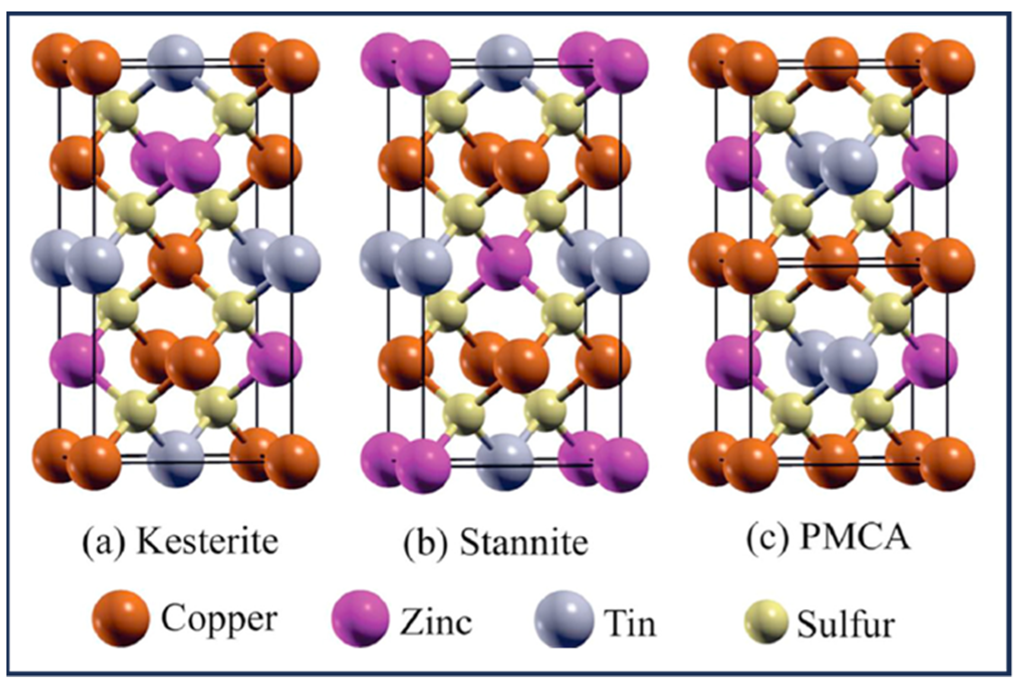
Figure 1. CZTS crystal structures of kesterite, stannite, and PMCA. Adapted from [21].
Crystals 14 00479 g001
Figure 2. The Cu2ZnSnS4 chemical potential phase diagram (under Cu-rich conditions). Adapted from [19].
Crystals 14 00479 g002
Figure 3. Quaternary phase diagram of Cu2ZnSnS4. Adapted from [62].
Crystals 14 00479 g003
Figure 4. (a) Schematic diagram of hydrothermal synthesis of CZTS nanoparticles. Created by Biorender.com. (b) FE-SEM images of CZTS with hierarchical structure. Adapted from [69]. (c) SEM images of CZTS quantum dots synthesized by hydrothermal method. Adapted from [68]. (d) TEM of as-synthesized CZTS nanoparticles. Adapted from [66]. (e,f) High-magnification TEM image of the CZTS nanocrystals synthesized by hydrothermal method. (e) Spherical nanocrystals. (f) Rod-like nanocrystals. Adapted from [70].
Crystals 14 00479 g004
Figure 5. (a,b) SEM images of CZTS nanoparticles synthesized by microwave-assisted solvothermal method, with (a) flower-like morphology of the sample with 2 mM precursor concentration, (b) sphere-like morphology of the sample with 10 mM precursor concentration. Adapted from [74], (c,d) TEM analysis of CZTS nanoparticles synthesized by solvothermal method at 250 °C for 2 h with (c) from chloride precursors, and (d) from acetate precursors. Adapted from [75].
Crystals 14 00479 g005
Figure 6. (a) Schematic diagram of sol–gel synthesis method. Reprinted with permission [103]. (b) Polydispersed CZTS nanocrystals with the crystalline size estimated at about 10–20 nm. Adapted from [78]. (c) TEM micrograph of the synthesized powder by sol–gel method. Reprinted with permission [79]. (d) SEM image of single-phase CZTS 3 layers film surface. Adapted from [80].
Crystals 14 00479 g006
Figure 7. (a) Schematic of the co-precipitation method, created by Biorender.com, (b) TEM image of slightly irregular and poly-dispersed of CZTS nanocrystals with average size of 10 nm synthesized by co-precipitation method. Adapted from [81], (c) SEM image of a sample synthesized by co-precipitation method using thiourea as a sulfur source. Adapted from [82].
Crystals 14 00479 g007
Figure 8. (a) Schematic of the hot-injection method, created by Biorender.com (b,c) TEM images for CZTS synthesized by hot-injection method, (b) using TOPO and TOP as the ligands, (c) using n-butylamine and octadecene as ligands. Adapted from [83].
Crystals 14 00479 g008
Figure 9. TEM images and corresponding SAED patterns of CZTS nanoparticles with (a) BA as capping ligand and TOP-S as sulfur source, (b) OA as capping ligand and TOP-S as sulfur source, (c) BA as capping ligand and 1-DDT as sulfur source, (d) OA as capping ligand and 1-DDT as sulfur source. Adapted from [86].
Crystals 14 00479 g009
Figure 10. (a) Schematic of OM-assisted colloidal synthesis method of CZTS nanoparticles and the structural evolution, (b,c) TEM images of CZTS nanoparticles synthesized by one-step colloidal method, (b) CZTS-0: 2-D nanosheet structured sample, (c) CZTS-3: nanorod structured sample. Adapted from [88].
Crystals 14 00479 g010
Figure 11. SEM images of the surface of Cu2ZnSn(SxSe1−x)4, (a) x = 1, (b) x = 0.0, and (c) x = 0.4. Adapted from [89].
Crystals 14 00479 g011
Figure 12. (a) Schematic of the mechanical alloying process, created by Biorender.com (b) FEG-SEM, and (c) FEG-TEM of synthesized CZTS powders at 250 °C for 1 h. Adapted from [30].
Crystals 14 00479 g012
Figure 13. (a) Steps of spin-coating method, (b) SEM images of non-stoichiometric CZTS films coated at spinning speeds of 3200 rpm, (c) stoichiometric CZTS films coated at spinning speeds of 3200 rpm. Adapted from [119].
Crystals 14 00479 g013
Figure 14. (a) Flow diagram for the fabrication process of CZTS sensitized ZnO/ZnSe core/shell nanorods arrays and their application in liquid junction solar cells, (b,c) FE-SEM of: (b) Al:ZnO nanorods, (c) Al:ZnO/ZnS core/shell nanostructures. Adapted from [123].
Crystals 14 00479 g014
Figure 15. (a) Schematic of the spray pyrolysis method, created by Biorender.com, (bd) SEM surface images of CZTS thin films fabricated by spray technique on substrate with annealing temperature of (b) 250 °C, (c) 300 °C, and (d) 350 °C. Adapted from [79].
Crystals 14 00479 g015
Figure 16. (a) Schematic of thermal evaporation method. Adapted from [56], (bd) SEM images of CZTS thin film deposited by thermal evaporation method (b) as deposited, (c) annealed under vacuum, and (d) annealed under sulfur atmosphere followed by vacuum. Adapted from [129].
Crystals 14 00479 g016
Figure 17. (a) Schematic of the electron beam evaporation method. Adapted from [133], (be) FE-SEM images of CZTS thin films deposited by electron beam evaporation method on substrate at (b) 220 °C, (c) 250 °C, (d) 280 °C, and (e) 310 °C. Adapted from [133].
Crystals 14 00479 g017
Figure 18. Schematic of successive ionic layer adsorption and reaction (SILAR) method. Adapted from [134].
Crystals 14 00479 g018
Figure 19. (a) Schematic of PLD method of thin film deposition. Adapted from [56], (bd) FESEM images of CZTS thin films fabricated by PLD method and annealed at 550 °C in various atmospheres; (b1b3) Ar, (c1c3) N2, (d1d3) S. Adapted from [138].
Crystals 14 00479 g019
Figure 20. (a) Schematic of a typical setup for electrochemical deposition method, created by Biorender.com, (be) SEM images of CZTS thin films deposited by electrochemical method followed by sulfurization process at (b) 350 °C, (c) 375 °C, (d) 400 °C, and (e) 425 °C. Adapted from [142].
Crystals 14 00479 g020
Figure 21. Relationship between the size of CZTS NCs and the bandgap energy (E). Solid lines represent the results of calculations in the frame of the effective mass approximation using different sets of m*e and m*h, scattered dots represent reported experimental results. Adapted from [166].
Crystals 14 00479 g021
Table 1. Various synthesis methods to synthesize CZTS/Se nanocrystals along with their preparation conditions.
MethodsNanoscale CZTS/Se Precursor MaterialsConditionsRef.
HydrothermalCZTS nanoparticlesCuCl2, ZnCl2, SnCl2, and Na2SAt 230 °C for 24 h, different concentration ratios of Na2S as the sulfur source, and CuCl2 as the copper source[66]
CZTS pure kesterite structure nanoparticles with size 20–30 nmCuCl2, ZnCl2, SnCl2, and Na2SAt 220 °C for 12, 18, and 24 h[67]
CZTS Quantum Dots with size of 10.74 nm and 12.2 nmCuCl2, ZnCl2, SnCl2, and thiourea (CH4N2S)At 230 °C for 24 h, precursors in a molar ratio of 2:1:1:8 (Cu:Zn:Sn:S)[68]
CZTS hierarchical flower-like structureCuCl2, ZnCl2, SnCl2, and thiourea (CH4N2S)At 180 °C for 4, 8, 16 and 20 h[69]
CZTS nanoparticles with an average size 7 nm–60 nm, rod-shape, and spherical nanocrystal shapesCuCl2, ZnCl2, SnCl2, and thiourea (CH4N2S)At 200 °C for 72 h[70]
CZTS nanoparticles with the domain size between 5 and 6 nmCuSO4, Zn(NO3)2, SnCl2, thiourea (CH4N2S)At 200 °C for 1 h[71]
CZTSe nano-powders with polygon flakes morphology with thickness of about 30~40 nm and 50~200 nm diametersCuCl2, ZnCl2, SnCl2, and SeO2At 160–200 °C for different times (10–90 h)[72]
SolvothermalCZTS nanocrystals with the size of 6–9 nmCuCl2, ZnCl2, SnCl2, and thiourea (CH4N2S)At 160 °C, 180 °C, and 200 °C for reaction times of 6 to 24 h[73]
CZTS nanocrystals, change of the flower like morphology to spherical type by changing reactants concentrationCuCl, ZnCl2, SnCl4, and thiourea (CH4N2S)At 140, 160, 180 and 200 °C for 10, 20, 30, and 40 min,[74]
CZTS nanoparticles, An ellipsoidal to spherical shape growing from a mean size of 7 to 15 nm, respectively, from chlorides precursors, and 2–3 nm particle size from acetate precursorsSn(IV) acetate, Cu(II) acetate, Zn(II) acetate dehydrate, CuCl2, ZnCl2, SnCl2, CS2At 200 °C for 2 and 24 h, At 250 °C for 2, 4, 8, and 24 h, using different metal salt precursors[75]
CZTS spherical particles containing nanocrystals of 11–12 nm in diameterCuCl2, ZnCl2, SnCl2, and thiourea (CH4N2S)At 200 °C for 24 h[76]
CZTSe dispersed nanocrystals with size of 8–12 nmCuCl, ZnCl2, SnCl4, and Se powdersAt 200 °C for 24 h[77]
Sol–gelCZTS crystalline size of about 10–20Copper (II) acetylacetone, zinc (II) acetate, tin (II) chloride, and sulfide powder In argon protection atmosphere[78]
CZTS nanoparticles with sizes ranging between 2 and 4 nmCuCl2·2H2O, ZnCl2, SnCl2·2H2O, and CH4N2SAt 50–60 °C, without sulfurization and toxic atmosphere[79]
CZTS films with average crystallites size of 60 nmCuCl2, ZnCl2, zinc acetate, and thiourea (CH4N2S)Dissolved in dimethyl sulfoxide at room temperature[80]
Co-precipitationCZTS nanocrystals in the range of 8–10 nmcopper (II) acetate, tin (IV) acetate, zinc acetate, and thiourea Under N2 atmosphere[81]
CZTS crystalline size of 15–17 nmCupric (II) chloride, zinc (II) acetate, tin (II) chloride, thiourea ethanol as the sulfur anion sourceWater as a solvent without any surfactants, noble gases, and vacuum process.[82]
Hot-injection and colloidal synthesisCZTS nanoparticles, size between 2–5 nm, Agglomerated nanorods and nano spherical particlesCuCl2, ZnCl2, SnCl4, and sulfur powderUsing different ligands: Trioctylphosphine oxide, Trioctylphosphine, n-butylamine and Octadecene[83]
CZTS nanocrystals, average size of 4–9 nmCuCl2, ZnCl, SnCl2, and thioacetamideUsing oleylamine (OLA) as both the solvent and the nanocrystal stabilizer, different process time[84]
CZTS nanoparticles with an average diameter of 23 ± 11 nmCuCl2, zinc acetate, SnCl2, pure sulfur Ligand-free[85]
CZTS nanoparticles with different morphology from thin plates with hexagonal symmetry to triangular shaped nanoparticlesCuCl2, ZnCl2, SnCl4, Sulfur sources: 1-Dodecanethiol (1-DDT) and Trioctylphosphine-S (TOP-S)Various capping ligands and sulfur sources (ligands: butylamine (BA) and oleic acid (OA),[86]
CZTS rod-shape nanoparticlesCuCl2, ZnCl2, SnCl4, and sulfur powderDifferent Zn/Sn precursor ratio (Zn:Sn ratio as 1.2:1 2:1 and 4:1)[87]
CZTS nanocrystals from 2D nanosheets to 1D nanorodsCu(acac)2, Zn(acac)2, SnCl4, and 1-dodecanethiol (DDT)One-pot colloidal synthesis assisted by continuous addition of oleylamine (OM) as a surfactant[88]
CZTS/Se nanoparticlesCuCl2, ZnCl2, SnCl2, sulfur, and selenium powderCu2ZnSn (SxSe1-x)4 (x = 0.0, 0.4, 1.0)[89]
Solid state, Mechanical alloyingCZTS particles in range of 0.07–3.71 mmElemental powders of Cu, Zn, Sn, and SBall-to-powder weight ratio of 5:1, 50 Hz frequency, 300 rpm revolution speed and 600 rpm rotation speed, milling time of 10, 15, 20, 25, 30, 35 h[90]
CZTS nanoparticles, particle size in the range of 50–60 nmElemental powders of Cu, Zn, Sn, and S Ball-to-powder ratio of 10:1, milling speed 300 rpm, under Ar atmosphere for 16 h[30]
CZTSe and CZTS nanocrystalline powders, particle size distribution in the range of 133–286 nmElemental powders of Cu, Zn, Sn, S, and Se Ball-to-powder mixture weight ratio of 5:1, 450 rpm for 30 h, 1-Butanol added to the mixture as a wet medium to enhance the efficiency of ball milling and preventing the agglomeration[91]
CZTS nanocrystalline with grain size between 10 and 20 nmElemental powders of Cu, Zn, Sn, and S flakesBall-to-powder weight ratio of 100:1, ethanol as lubricant, time duration of 15, 30, 60, 90, and 180 min[27]
CZTS nano-powderElemental Cu, Zn, Sn, and S450 rpm for 30 h with butanol[92]
CZTS equiaxed nanoparticles with approximate size of 10 to 15 nmCu(acac)2, Zn(acac)2, SnCl2, and thiourea (CH4N2S)Milling with ethanol, synthesized in tubular furnace at 250 °C for 1–12 h in argon atmosphere[93]
CZTSe with crystalline size of 10–2 nmElemental Cu, Zn, Sn, and Se Ball-to-powder ratio of 5:1, various milling times[94]
Table 2. Thin film deposition techniques of CZTS/Se nanomaterials along with their process conditions.
Deposition MethodCZTS Thin Film MorphologiesConditionsRef.
Spin coatingCZTS thin film with different surface morphological characteristics Preheated in various atmospheres (air, Ar, and N2) before sulfurization at 580 °C[118]
CZTS thin film with various degrees of crystallizationVarious compositions, annealing at 500 °C in N2 atmosphere[119]
CZTS thin film with various surface morphologyAnnealing temperature in the range of 525 °C and 575 °C (under H2S gas atmosphere)[120]
Evolution of the CZTS thin film surface morphology from a non-crystallized, compact, uniform, and dense texture with cracks to an aggregated grains and nanoparticles with non-uniform distribution with porous textureAnnealing temperatures (300, 400, 500 and 550 °C)[121]
CZTS thin film with different roughness and closely packed surfaceSol–gel spin coating doped by Cd and Mg, and followed by sulfurization[104]
CZTS thin film with crystallite size of 7.02, 7.74, and 9.09 nm, crystallite number of 2.31, 2.03, and 1.26 × 10¹⁸ (m−2)Annealing in air at 300 °C and duration times of 5, 10 and 20 min[122]
Core/shell vertically aligned nanorods arrayCondition is briefly described in the spin-coating section[123]
Spray pyrolysisCZTS thin film with stannite structureSprayed at a flow rate of 2.5–3.0 mL·min−1 using a nitrogen gas flow of 3.2 mL·min−1 for 90 min, heated to 280–360 °C[124]
CZTS film with different crystallinitySubstrate temperature (563–723°K), without annealing and post-deposition sulfurization[125]
CZTS thin film surface with micro-crystallites range from 0.02 to 0.2 μmSprayed for 30 min and 60 min on substrates with temperature from 553°K to 633°K[126]
CZTS thin film with inhomogeneity and the phase segregationSubstrate temperature of 325 °C, sulfurization at 550 °C with elemental sulfur in an Argon atmosphere[127]
CZTS film with various surface morphology from agglomerations of small grains with some voids to dense surface with the porous structure and significantly clear grainsSubstrate temperature of 250, 300, and 350 °C[79]
Thermal EvaporationCZTS film with different phase formation and phase purityPost-deposition annealing at 300, 400, 450, 500, and 550°C for 15 min, sulfurization at 500 and 550 °C for 15 min[128]
CZTS film with different surface morphology from flat and smooth with negligible grains to a homogeneous and compact surface with densely packed grainsNon-heated substrate, post-deposition annealing under different atmospheres: (1) vacuum annealing, and (2) sulfur annealing followed by vacuum annealing[129]
Polycrystalline CZTS thin film with tetragonal crystal structureUsing CZTS nano-structured materials synthesized by different solvent (water, ethylene diamine, and ethylene) for the deposition process, post deposition annealing at 450 °C in nitrogen atmosphere for 1 h[130]
Electron Beam EvaporationCZTSe thin filmHot pressed near stoichiometric CZTSe as the bulk source, electron beam current varied between few mA to 110 mA without any post deposition annealing[131]
Sandwich device (Al (50 nm)/CZTS (80 nm)/Al (50 nm))Deposited with depositing rate of 0.5 nm/S at room temperature[132]
CZTS film with different surface morphology from rough surface with many pinholes to large grain size surrounded by smaller grainsDeposition of the CZT precursors on pre-heated substrates followed by a sulfurization, deposition rate of ~10 nm s−1, substrate temperatures of 220, 250, 280 and 310 °C[133]
SILARCZTS thin films, surface morphology from non-uniform distribution of agglomerated particles to many larger CZTS particles with uniform average grain size of 100 nmCuSO4, ZnSO4, SnSO4, and Na2S dissolved in H2O, 10, 20, 30, and 40 number of immersion cycles with immersion time of 30 s[134]
Phase pure CZTS thin flmsSeparate bath for Zn2+ ions to avoid formation of Cu3SnS4 (CTS) and Cu2S phases, followed by annealing at elevated temperature[135]
Homogeneous CZTS films with nano-crystalline agglomerated spherical-like particles, well distributed over the surface Different dipping times, conducting and nonconducting substrates, followed by annealing at 400 °C[136]
Compositional pure CZTS thin filmVarius precursor concentration, dipping time and number of cycles (30, 40, and 50 cycles), annealing in Ar atmosphere at 250 °C for 4 h[137]
PLDHomogeneous composition CZTS thin filmAnnealing at 550 °C in different atmospheres (Ar, N2, and S powder)[138]
Single-phase stannite CZTSe thin filmSubstrate temperatures varied from room temperature to 500 °C[139]
Cu2−xPbxZnSnSe4 (x = 0, 0.06 and 0.18) and Cu2ZnSn1−yTiySe4 (y = 0, 0.1. 0.3 and 1.0) thin filmsModified target with Pb and Ti, selenization carried out at 450 °C for 30 min[140]
Electrochemical Deposition methodCZTS thin filmDifferent standard electrochemical potentials, under N2 atmosphere, different bath composition[141]
CZTS thin film with different grain formation and crystallizationSulfurization in N2 + H2S atmosphere at different temperatures of 350, 375, 400, and 425 °C for 10 min[142]
Uniform and compact CZTS thin filmDeep eutectic solvent (named Reline) as a green electrolyte, in a mixture of H2S and N2 at 550 °C for 1 h[143]
CZTSe thin film consist of nanocrystals with size of 25–50 nmAt a constant potential of 0.6 V for 30 min at room temperature[144]
Disclaimer/Publisher’s Note: The statements, opinions and data contained in all publications are solely those of the individual author(s) and contributor(s) and not of MDPI and/or the editor(s). MDPI and/or the editor(s) disclaim responsibility for any injury to people or property resulting from any ideas, methods, instructions or products referred to in the content.