1. Introduction
Thick films of piezoelectric ceramics are of particular interest for vibrational energy harvesting systems [
1,
2,
3,
4] due to their ability to convert mechanical vibrations into electrical energy, which can be used to power devices for the Internet of Things [
5], such as remote unattended wireless sensors. In addition, ceramic thick films also find use in various other technologies, such as coatings for biomedical applications [
6], photocatalysis [
7], high energy density energy storage capacitors [
8], solid-state batteries [
9], and solid oxide fuel cells [
10], amongst others [
11,
12]. Powder aerosol deposition (PAD) is especially attractive for depositing these films as it is a rapid, room temperature process that allows for the deposition of thick films (approximately 1 µm to >100 µm) directly onto the substrate on the scale of minutes, as well as the combination of various material classes, such as ceramics [
13], glasses [
14], metals [
15], semi-conductors [
16], and some polymers [
17,
18].
Despite its apparent advantages, however, there are several significant drawbacks to this process that are the focus of ongoing research. Firstly, there is the development of significant internal residual stress during deposition, which has been previously characterized by various researchers [
19,
20,
21,
22,
23]. These internal biaxial stresses can range from approximately 300 MPa to 2 GPa, depending on various factors, such as the deposited material, substrate, deposition parameters, and carrier gas [
19,
20,
21,
22,
23]. Interestingly, it has been previously demonstrated that the internal stress is not due to film/substrate interactions; rather, the internal stresses are locked inside the film during the deposition process and are maintained even after the film is removed from the substrate [
24], which corresponds to observed residual stress in the metal substrates at the surface through plastic deformation [
25]. Importantly, however, the internal residual stress in the film can be significantly reduced through thermal annealing [
23], suggested to be due to the reorganization of local grain boundary defects at elevated temperatures. Oxygen was found to play a particularly important role, whereby reincorporation of oxygen along the grain boundaries is suggested to occur. Eckstein et al., for example, developed a method to produce freestanding films (FSFs), which displayed nonlinear, remanent shrinkage during heating, which is understood to be due to local chemical redistribution and changing oxygen vacancy concentration [
24]. Secondly, the conductivity of ceramic films in the as-processed state has been observed to vary from the bulk [
10,
26], reducing the functional properties necessary for electrical applications such as vibrational energy harvesters. Thermal annealing has also been demonstrated to influence conductivity, which is related to the changing concentration of defect-related charge carriers, such as ionic vacancies and crystalline defects like dislocations, deposition-induced amorphous regions, as well as interdiffusion with the substrate at elevated temperatures [
10,
26]. The internal residual stress and conductivity, however, can be controlled to some extent through aliovalent doping of the deposited material as well as thermal annealing in different atmospheres [
27].
The final issue is that the resulting ceramic thick films have a nano-grained microstructure from the impact consolidation process [
28]. During deposition, micron-sized particles are accelerated at the substrate through a nozzle, where they impact the substrate and can break apart and adhere to the substrate and one another in an additive process. This results in large, localized stresses that result in the formation of nano-sized grains through the fracture of micron-sized particles [
14,
29]. Importantly, it is well-known that the piezoelectric and ferroelectric response is significantly limited during the reduction in grain size [
30,
31], which is related to the reduction in the extrinsic contributions to the electromechanical properties [
32]. As piezoelectric materials are used extensively in vibrational energy harvesting systems [
2,
33], the grain size will also have an important influence on the energy generation capabilities of PAD films. As such, previous researchers have used thermal annealing to increase the grain size of the PAD films [
34,
35,
36], corresponding with an increase in the crystallite size and a decrease in the macrostrain of the film [
26,
37], which results in enhanced piezoelectric, dielectric, and ferroelectric properties [
34,
35,
37]. It is important to mention, however, that the substrate is a significant limiting factor, either due to the limited high-temperature stability of the metal substrate or the mismatch of the coefficients of thermal expansion (CTE) between the film and substrate, leading to the loss of film integrity. Bentzen et al., for example, showed through time-of-flight secondary ion mass spectroscopy and energy-dispersive X-ray spectroscopy that there is a chemical reaction with the substrate at high temperatures, and certain elements, such as chromium, can act as a sintering aid that enhances grain growth [
36]. As such, the annealing process might lead to interdiffusion [
10,
36] and changes in the stress state [
23], resulting in defects in the film and thus reducing the functional properties. Therefore, various local annealing methods have been investigated to selectively heat the film, such as laser annealing [
38]. Importantly, however, these previous studies on annealing of PAD films to enhance the grain size were primarily focused on ceramic films attached to substrates, which limited the maximum temperature that could be applied and made it difficult to directly observe the film response without the substrate interaction effects. Hoshina et al. [
39], for example, investigated the annealing effects on functional properties of BaTiO
3 FSFs, demonstrating a significant enhancement in the dielectric and ferroelectric properties corresponding to an increase in the grain size. During this study, however, they produced FSFs by using the difference in CTE between the deposited film and single crystal SrTiO
3 substrate, detaching the film at 600 °C. This means that the film was already thermally annealed prior to electromechanical measurements. In addition, this technique relies on variations in CTE between the film material and substrate, making it likely not applicable to all materials of interest.
In this work, (Ba,Ca)(Zr,Ti)O
3 (BCZT), a lead-free ferroelectric with an excellent piezoelectric response (
) [
40], was used to fabricate FSFs in order to investigate the role of grain growth on the electromechanical response in PAD thick films without the influence of the substrate [
41]. Freestanding films were produced using a NaCl-BCZT sacrificial layer that allowed for the removal of the BCZT thick film without thermal treatment. Similar methods were previously applied to powder aerosol deposited films to detach them without thermal treatment, preserving their as-processed state [
24,
27]. These previous studies, however, did not consider the influence of high-temperature annealing to induce grain growth. Following this, the thermal expansion of the resulting films was characterized as a function of atmosphere. In addition, the temperature-dependent dielectric response as well as the room temperature macroscopic ferroelectric properties of FSFs were determined as a function of annealing temperature from 800 °C to 1400 °C to investigate the role of grain size. Data were compared to the bulk response, where notable variations were observed.
2. Experimental Methodology
Ba0.85Ca0.15Zr0.1Ti0.9O3 powder was synthesized for powder aerosol deposition using the solid–state reaction method. For this, the raw powders BaCO3 (99.8% purity, Alfa Aesar, Haverhill, MA, USA), CaCO3 (99.5% purity, Alfa Aesar), ZrO2 (99.7% purity, ThermoFisher Scientific, Waltham, MA, USA), and TiO2 (99.6% purity, ThermoFisher Scientific) were dried at 120 °C to remove humidity and subsequently stoichiometrically weighed in a glove box with controlled humidity of <10% to limit issues with moisture absorption. A balance (MSE124S-100-DU, Sartorius AG, Göttingen, Germany) enabled precise weighing with an accuracy of 0.1 mg. Subsequently, 100 g of ethanol and 820 g of zirconia milling balls (with a diameter of 5 mm) were added to a polyethylene bottle and placed on a rolling bank under a slight angle on the rotational axis for mixing and homogenization of the raw powders. The rotational speed was adjusted to 20 rpm and kept for 24 h. Then, the slurry was dried with a rotational evaporator (Rotavapor R-300, Büchi Labortechnik AG, Flawil, Switzerland). The resulting powder was ground for 15 min with a mortar and pestle and further dried for 1 h at 120 °C. Finally, the powder was calcined in a high-temperature oven (HTC08/15, Nabertherm GmbH, Lilienthal, Germany) at 1350 °C for 3 h with a heating and cooling rate of 5 K/min. Following particle size measurements (Partica LA-960, HORIBA, Kyoto, Japan), the calcined BCZT powder was milled for 4 to 8 h on the same roll bank with a rotational speed of 20 rpm for homogenization and to produce the correct particle size distribution for powder aerosol deposition. A median particle size d50 of approximately 1.3 μm was targeted.
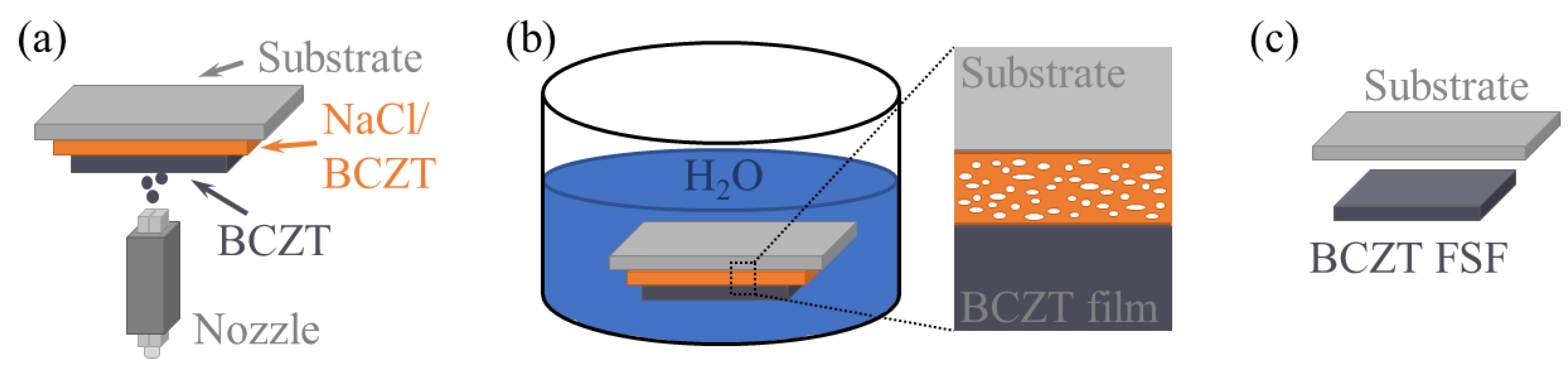
The BCZT and sacrificial composite BCZT/NaCl films were deposited on mirror-polished 20 mm × 20 mm SUS 304 stainless steel substrates using N2 carrier gas (99.999% purity) with a flow rate of 4 and 5 L/min, respectively, with a nozzle-to-substrate distance of 3 and 5 mm, respectively. Both films used a scanning speed of 5 mm/s, whereby the BCZT/NaCl sacrificial film had four scans and the BCZT had up to 5000, which was found to be necessary to produce the required 90 µm film thickness. A converging slit nozzle with a geometry of 1 mm × 10 mm was used for all deposition steps. A BCZT/NaCl composite layer was used as a sacrificial layer, as it was observed that the BCZT was required to maintain stability during deposition of the BCZT film on the sacrificial layer and ensure that the NaCl coating was not removed during the PAD process.
Once the desired BCZT thickness was reached, which was confirmed by a line scanning laser profile measurement device (UBM Messtechnik GmbH, Ettlingen, Germany), the samples were submerged in distilled water for at least 12 h to dissolve the NaCl and form a porous sacrificial film (
Figure 1). After drying the samples, the steel substrate was bent to break the porous sacrificial film and release the FSFs for further processing and measurement. The obtained BCZT FSFs were annealed in a temperature range from 800 °C to 1400 °C with a temperature step of 100 °C. The dwell time was adjusted to 5 h, with a heating and cooling rate of 1 K/min to prevent cracking due to high thermal stress. For comparison, an 80 µm-thick BCZT PAD film without a sacrificial layer was fabricated with the same procedure. Reference bulk samples were fabricated by conventional sintering at 1450 °C for 3 h with a heating and cooling rate of 5 K/min and subsequent grinding to a thickness of 1 mm. To remove stress induced during processing, the samples were annealed at 500 °C for 1 h with heating and cooling rates of 2 K/min and 1 K/min, respectively.
The grain sizes of the FSFs were analyzed on the top and bottom surfaces of the films. The unpolished top sides of the FSFs annealed at 1000, 1100, 1200, 1300, and 1400 °C, as well as the bulk samples, were analyzed by a scanning electron microscope (SEM, Quanta 200, FEI Co., Hillsboro, OR, USA), whereas the bottom surfaces of the FSFs annealed at 800, 900, 1000, and 1100 °C, as well as the as-processed sample, were ion milled to prepare around 50 nm-thick slices, which were investigated by a transmission electron microscope (TEM, JEM-ARM200F, JEOL Ltd., Frenchs Forest, Australia). The grain sizes of all samples were determined from the obtained images using the linear intercept method and the Ferrel method, as well as the image software, Fiji (version 1.54i), conducting two measurements on at least 100 grains per sample and per investigated surface.
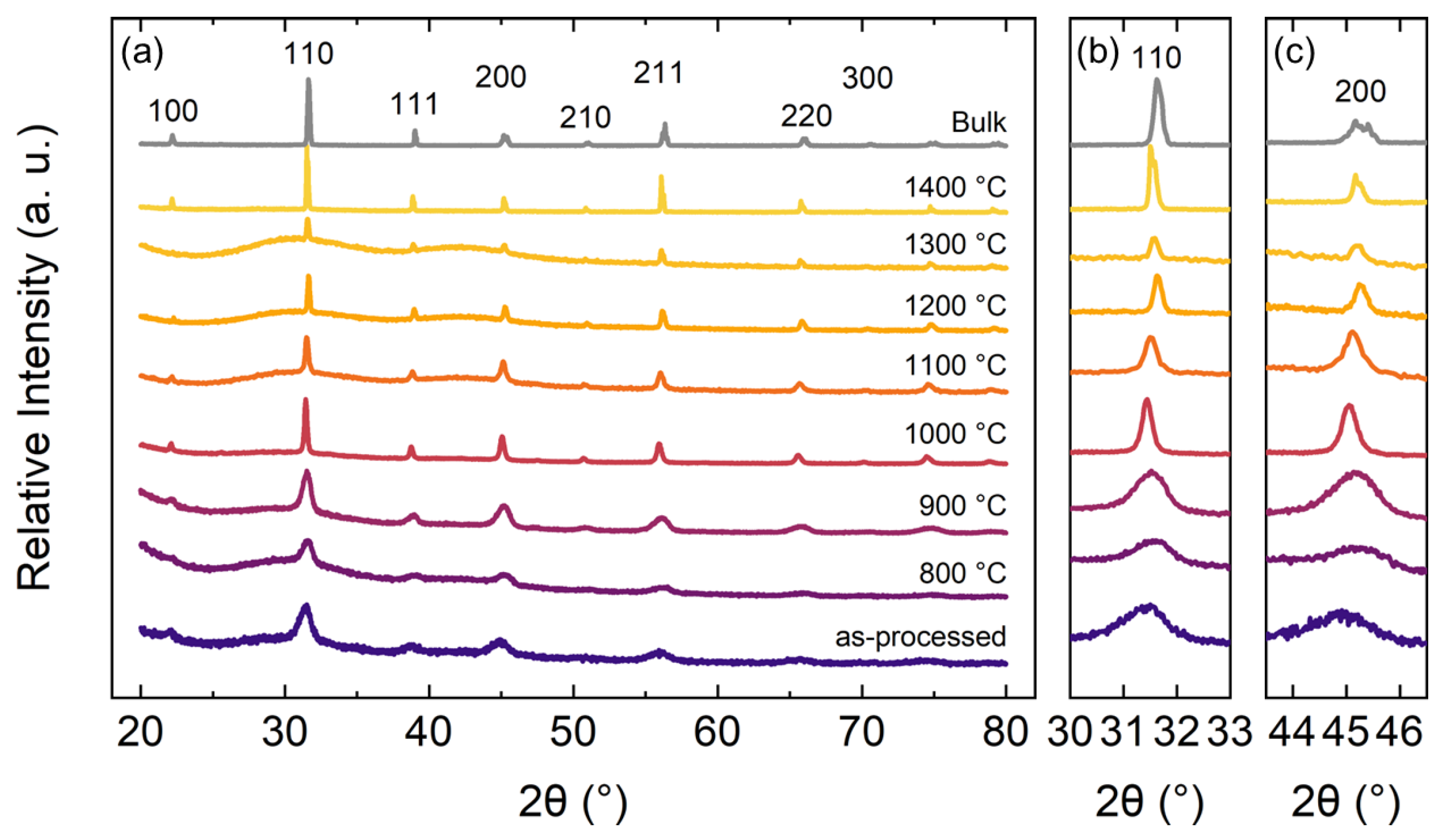
The room temperature crystal structures of the films and the reference bulk sample were analyzed by an X-ray diffractometer (Bruker D8 ADVANCE Eco, Brucker AXS, Karlsruhe, Germany), equipped with a Cu Kα source operating at 25 mA and 40 kV. Diffraction patterns were recorded in the Bragg–Brentano geometry using a position-sensitive detector LYNXEYE XE in a 2θ range from 20° to 80° with a step of 0.02° and a time of 1 s per step. The selected area peak fitting method was used to identify the peak broadening, i.e., full width at half maxima (FWHM) of the 200 reflection.
25 nm-thick Pt electrodes were sputtered on the samples using a sputter coater (Q150T plus, Quorum Technologies, Lewes, UK) with a sputter current of 30 mA and a time of ~3 min under an operational vacuum of 0.009 mbar. Non-adhesive polyimide tape was used as a sputtering mask. Care was taken to ensure that the top and bottom electrode areas of the FSFs were of equal size and positioned above one another. Optical microscope images of each electrode site were recorded and used to verify the overlapping electrode area. Following this, the temperature-dependent dielectric behavior of the BCZT bulk samples and the PAD reference film was characterized in a custom-built oven with electrical contacts (LE 4/11 3216, Nabertherm GmbH) up to a maximum temperature of 200 °C with a heating and cooling rate of 2 K/min. FSFs were measured using a temperature-controlled stage with four-point electrical contacts (HFS 600E-PB4, Linkam Scientific Instruments Ltd., Redhill, UK). During heating, the FSFs were placed on a sapphire slide that was sputtered with a platinum layer, which served as the bottom electrode. Two tungsten probes were contacted to the bottom electrode, and another two tungsten probes were contacted to the top FSF electrode, resulting in a four-point measurement. The thermal chamber was gas-tight, and air as well as N2 gas (99.999% purity) were used during high-temperature measurements. Temperature was monitored by an external controller inside the gas-tight thermal chamber. In addition, BCZT and BaTiO3 bulk samples were measured in both setups to determine a temperature calibration curve. For this purpose, phase transition temperatures and maximum permittivity temperatures were compared. A linear regression model was fitted to the data points, allowing for temperature corrections for subsequent measurements. For both heating systems, an LCR meter (E4980AL, Keysight Technologies, Santa Rosa, CA, USA) was used to determine the dielectric response as a function of frequency from 100 Hz to 1 MHz. Custom LabVIEW software (based on version NXG 5.1, National Instruments, Austin, TX, USA) was used to measure and evaluate relative permittivity and dielectric loss.
The large field polarization–electric field response of the FSF samples was characterized with a commercially available ferroelectric tester (TFAnalyzer 2000, aixACCT Systems GmbH, Aachen, Germany). Using a high-voltage amplifier (Model 20-20C-H, Advanced Energy Inc., Fort Collins, CO, USA), a 100 Hz triangular waveform with a maximum electric field of 3 kV/mm was applied to bulk samples and FSFs annealed above 1000 °C, whereas FSFs annealed up to 1000 °C were applied with 20 kV/mm.
3. Results and Discussion
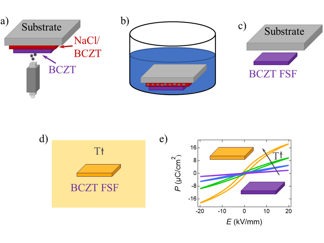
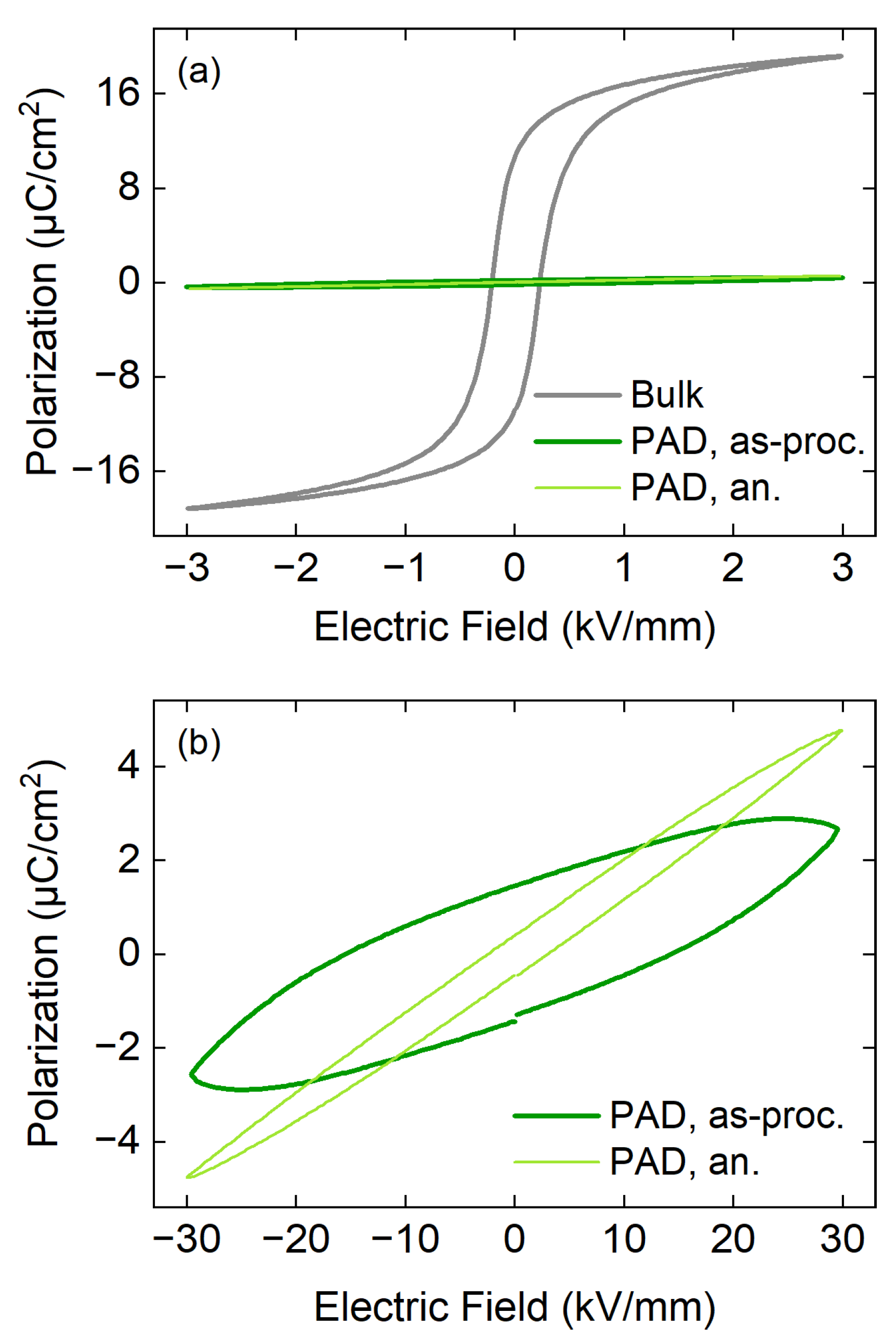
Despite the advantages of PAD in producing ceramic thick films rapidly at room temperature, such thick films display a nano-grained structure that can significantly limit the functional properties [
34]. Other effects, such as internal residual microstrain [
37] and increased conductivity, are also important but can be mitigated to some extent through annealing at elevated temperatures. To illustrate this,
Figure 2 shows the large field polarization–electric field hysteresis of a bulk BCZT sample compared to PAD films of the same BCZT composition, clearly showing a significant decrease in the ferroelectric response. Here, the PAD films were measured in the as-processed as well as the annealed state (500 °C, 1 h), where a decrease in film conductivity can be observed after annealing through the formation of a slimmer hysteresis loop. It is important to note, however, that the annealed sample also displays a near-linear dielectric response without polarization saturation at the applied maximum electric field values. The amount of extrinsic contributions also remain unclear in PAD films. Previous studies have shown that under elevated electric fields, polarization saturation can be achieved, with the maximum polarization being dependent on the annealing temperature [
34,
35]. It has been demonstrated, for example, that as the annealing temperature increases and approaches the sintering temperature, grain growth can occur in ferroelectric films. This microstructural change enhances the ferroelectric response, approaching the behavior observed in bulk samples [
34,
35].
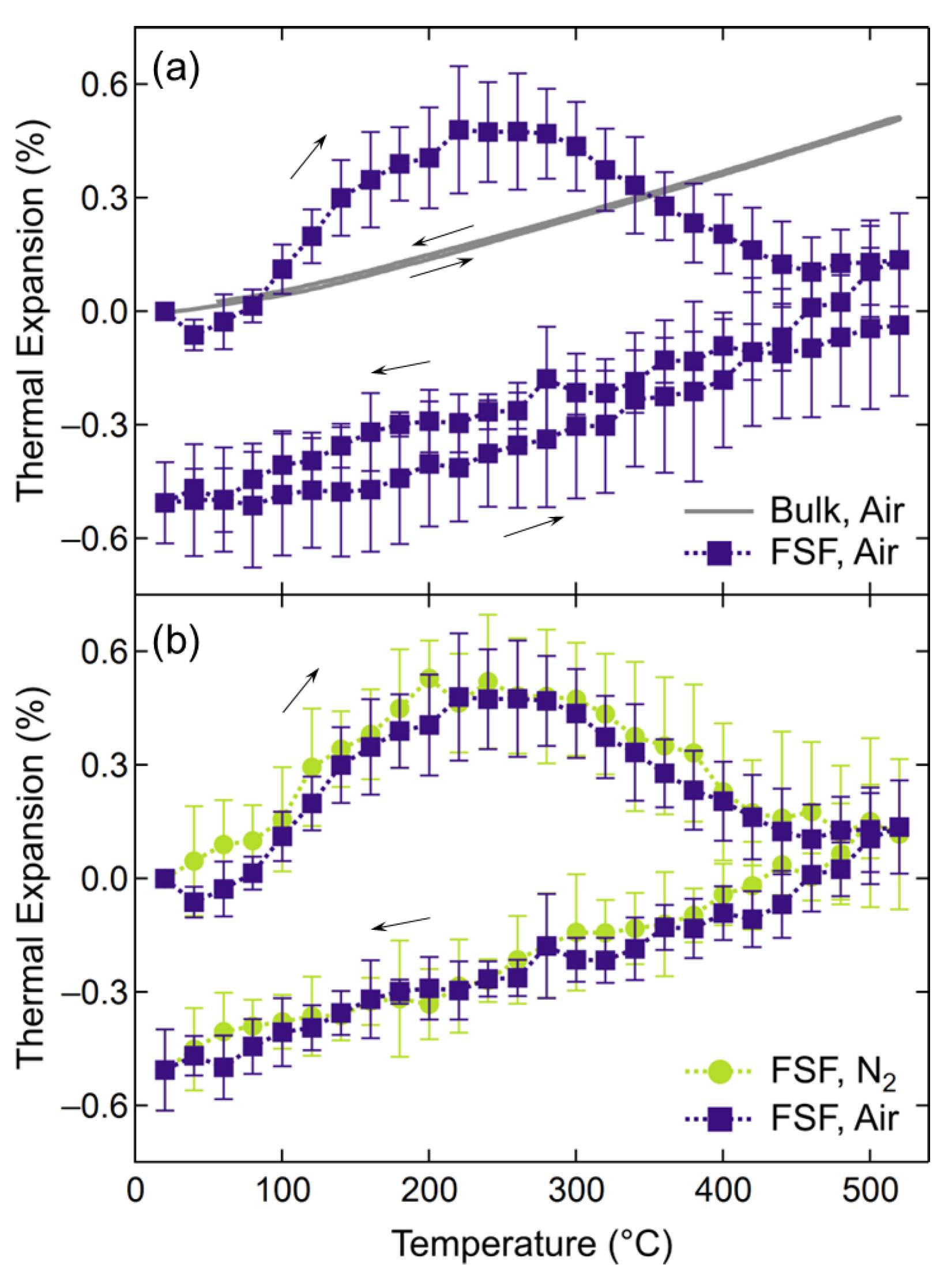
It is understood that the increased ferroelectric hysteresis in as-processed ceramic thick films is related to the formation of grain boundary defects during the deposition process, which has been shown to correspond to remanent temperature-dependent shrinkage [
27]. The exact nature of the grain boundary defects remains under debate but likely involves cationic and anionic defects, including vacancies, which may be related to the formation of a possible space charge layer [
42]. Through the characterization of thermal expansion with different partial pressures of oxygen, previous work demonstrated that the observed shrinkage is likely due to the (i) local reorientation of grain boundary defects, which appears largely independent of the oxygen partial pressure, and (ii) the reincorporation of oxygen from the surrounding atmosphere [
27], although the crystallization of amorphous phases might also contribute [
26]. Here, the thermal expansion of BCZT FSFs was characterized up to approximately 520 °C in different atmospheres (
Figure 3). During heating from the as-processed state in air, there is an initial almost linear expansion up to approximately 220 °C, resulting in a CTE value of around 24
10
−6/K. To determine if this is due to the coefficient of thermal expansion of BCZT, a bulk BCZT sample was characterized in air using a dilatometer with the same heating conditions, revealing a CTE value of approximately 10 × 10
−6/K. The deviation between the FSFs and the bulk sample remains unclear. Above approximately 220 °C, the BCZT FSF displays a nonlinear decrease in thermal expansion, consistent with previous data on BaTiO
3 and Al
2O
3 [
27]. This effect begins to saturate with further increasing temperature. Upon decreasing the temperature, there is a nearly linear decrease in thermal expansion with a slope consistent with the observed thermal expansion of the bulk sample (13
10
−6/K), resulting in remanent shrinkage of approximately −0.5%. The observed shrinkage can be related to the reduction in cationic and anionic vacancies as well as the crystallization of amorphous regions in the AD film [
26]. Importantly, depending on the thermal expansion of the substrate, this effect can lead to variation in internal residual stress, which may affect the film’s properties. For example, Hoshina et al. [
39], used the variation in the thermal expansion of a BaTiO
3 film and SrTiO
3 single crystal substrate to produce sufficient stress to form an FSF at 600 °C. Similarly, Kawakami et al. observed variation in the piezoelectric response of BaTiO
3 thick films with different substrate materials [
19]. During the subsequent second cycle, the FSF only displays an approximately linear thermal expansion response (9
10
−6/K) without additional thermal shrinkage observed during the first cycle.
Previous work showed that the increased partial pressure of oxygen can lead to enhancement in the thermal shrinkage of BaTiO
3 films, which is understood to be due to the reincorporation of oxygen to fill oxygen vacancies [
24,
27]. However, there was no significant difference in the thermal expansion behavior of BCZT films characterized in air and in N
2 (
Figure 3b), similar to observations in Al
2O
3 [
27], which clearly indicated that oxygen reincorporation plays a minor role in thermal expansion behavior. It has also been shown that thermal expansion can be changed through aliovalent doping [
24], which varies the concentration of oxygen vacancies in perovskite ferroelectrics [
43]. Additional work is required to understand the role of defects and non-stoichiometry on the shrinkage of PAD thick films.
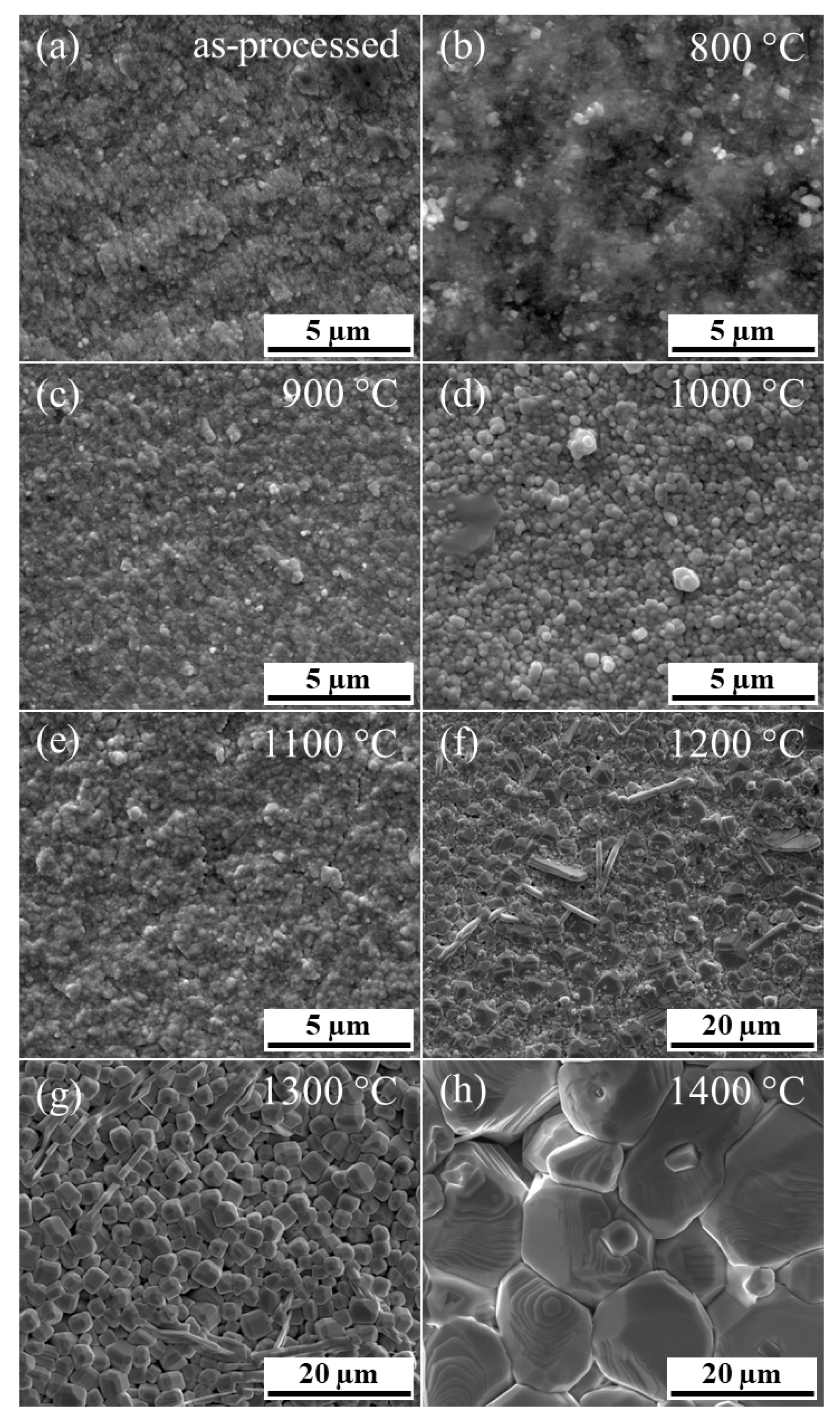
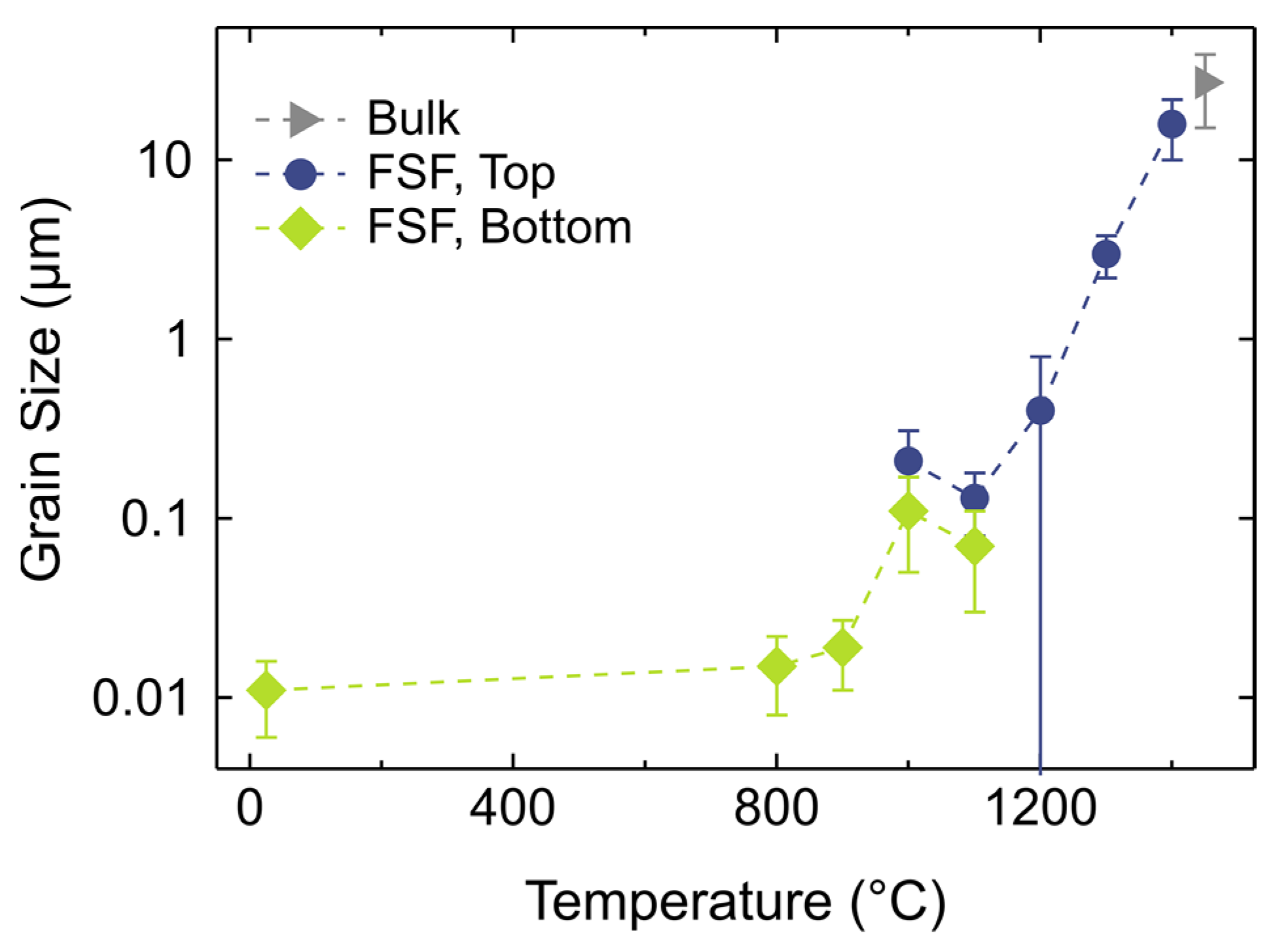
FSFs were annealed at various temperatures from 800 °C to 1400 °C, where SEM images of the resulting microstructures are shown in
Figure 4. There is an apparent grain size increase with increasing annealing temperature from nano-sized grains in the as-processed state to grains for samples annealed at 1400 °C of approximately 15.9 µm (±5.9 µm). In comparison, the grain size of the bulk BCZT samples was found to be approximately 27.1 µm (±11.9 µm). This corresponds well to previous studies that thermally treated PAD films [
19,
35,
37], although in these studies, the films were still attached to the substrates, meaning that film/substrate interactions could account for variations. In the present study, the FSFs were detached from the substrate and not subject to interaction with the substrate.
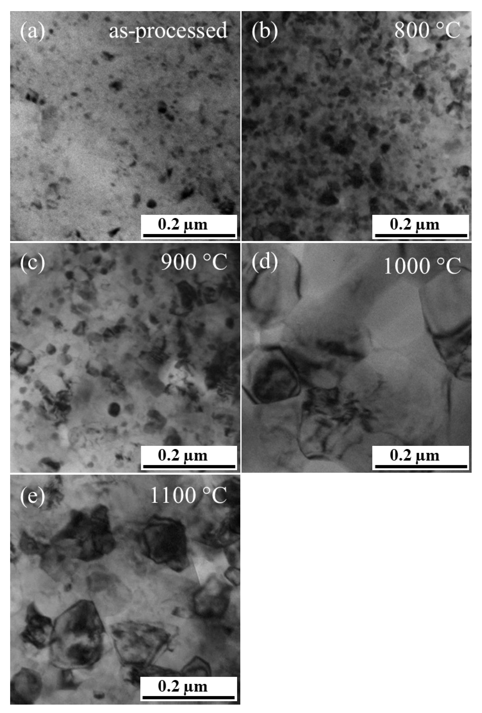
Due to the nano-sized grains in the as-processed FSF and those with lower annealing temperatures below 1200 °C, SEM could not be used to reliably determine the grain size. For this reason, TEM measurements were performed for FSF samples annealed up to 1100 °C (
Figure 5). The images were taken from the bottom of the FSFs, i.e., close to the interface of the sacrificial layer and the film. In contrast, SEM images were taken on the top surface of the FSFs. Here, variations in grain size distributions were observed, which are due to changes in the dynamic impact fracture of the particles with differences in the impacted surface, such as elastic properties. Similar to observations using SEM, TEM images also show an increase in the grain size with increasing annealing temperature.
SEM and TEM microstructural images were analyzed, and the grain size distributions for FSFs annealed at various temperatures were determined (shown in
Figure S1). It is important to note that due to the low thickness of the samples (~90 µm), the samples could not be polished. Although the microstructure should ideally be determined from an appropriately sectioned, polished, and etched area of the sample, it is expected that the general trend of the observed grain size distributions is representative. For FSFs annealed at 1000 °C and 1100 °C, grain size distribution was determined on the top of the sample using SEM and on the bottom of the sample with TEM. Interestingly, as previously noted, the observed grain size is smaller on the bottom surface, which is suggested to be due to properties of the impacted surface [
44]. Initially, BCZT particles impact an approximately 1 µm-thick sacrificial BCZT/NaCl layer, whereas the final particles impact an approximately 90 µm-thick BCZT film. This corresponds to previous observations of increasing surface roughness with film thickness [
20,
45], indicating that the impacting particles producing increasingly large impact crater-like surface impressions, which is likely due in part to the changing local properties of the film with thickness. Despite this, there is an apparent increase in the grain size with annealing temperature, where an annealing temperature of 1400 °C results in a grain size distribution comparable with the conventionally sintered bulk sample. In addition, the grain sizes of the FSF annealed at 1000 °C (0.16 µm ± 0.10 µm) was larger than those observed for an annealing temperature of 1100 °C (0.10 µm ± 0.06 µm). This is likely due to measurement variation; in total at least 100 grains were characterized from two different spots with SEM and TEM.
Figure 6 shows the average grain sizes as a function of the annealing temperature, where a clear increasing trend is observed. In particular, there are limited changes in the grain size between the as-processed and 800–900 °C states, after which a rapid increase in the grain size is observed. Interestingly, previous studies observed grain growth at lower temperatures than those observed here. For example, Bentzen et al. found significant grain growth with an annealing temperature of 750 °C in BaTiO
3 on a stainless-steel substrate [
36]. Similarly, Choi et al. also observed grain growth at 700 °C, which increased more significantly at 900 °C for Pb(Zn
1/3Nb
2/3)O
3–Pb(Zr
xTi
1−x)O
3 on sapphire substrates with Ag–Pd electrodes [
35]. In addition, Exner et al. also observed a marked increase in grain size with annealing temperatures of 600–700 °C for BiCuTiVO
x films [
26]. Importantly, these previous studies considered the growth of grain size in a film attached to the substrate and subject to annealing-induced thermal and chemical strains, as well as interdiffusion between the film and substrate. In the present study, the FSFs are detached from the substrate and do not have these interactions. In addition, it should be noted that BCZT has a relatively high sintering temperature for bulk samples of 1400–1500 °C [
40,
46], which is likely responsible for the observed limited grain growth until elevated temperatures.
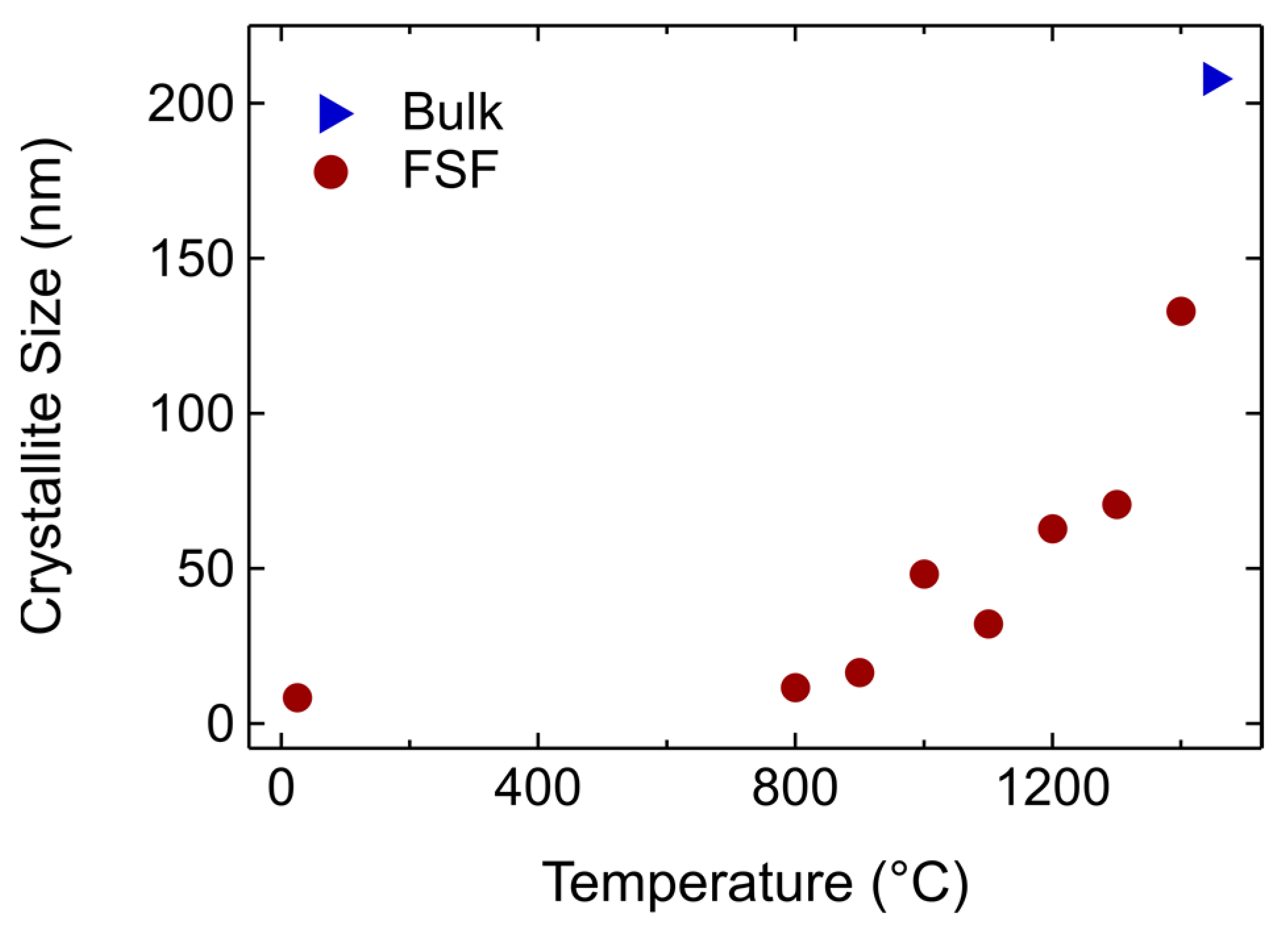
Following thermal annealing, the crystal structure was characterized using XRD at room temperature; diffraction patterns of bulk samples and FSFs are shown in
Figure 7. The as-processed film and all FSFs show principal Bragg reflections similar to the bulk samples. Interestingly, however, the distorted 200 reflection observed in bulk BCZT (
Figure 7c), an indication of orthorhombic and/or tetragonal symmetry [
47], is absent for all AD films. A similar observation has been reported for AD-processed BaTiO
3 films, where the absence of average crystal structure distortion is considered to be associated with the decrease in crystallite size [
24]. Please note that FSF specimens were only a few square millimeters in size; as such, the diffraction patterns have variable background contributions from the polymer sample holder and the modeling clay used to fix the sample. Nevertheless, this variable background did not influence the analysis of peak profile significantly. As can be seen from
Figure 7b,c, the diffraction peak width decreases with increasing annealing temperature. Analysis of peak width, i.e., sample-dependent line broadening contributions to the peak profile, can highlight the microstrain and broadening due to the decrease in the crystallite size [
48].
The crystallite size was calculated based on the Scherrer equation. It should be noted here that all diffraction data were collected using identical instrumental parameters. As the peak width is associated with both the crystallite size and microstrain, the increase in crystallite size is also accompanied by a decrease in microstrain [
49]. As such, the significant increase in crystallite size, as presented in
Figure 8, is associated with the change in annealing temperature above 900 °C, which matches well with the observed increase in grain size shown in
Figure 6.
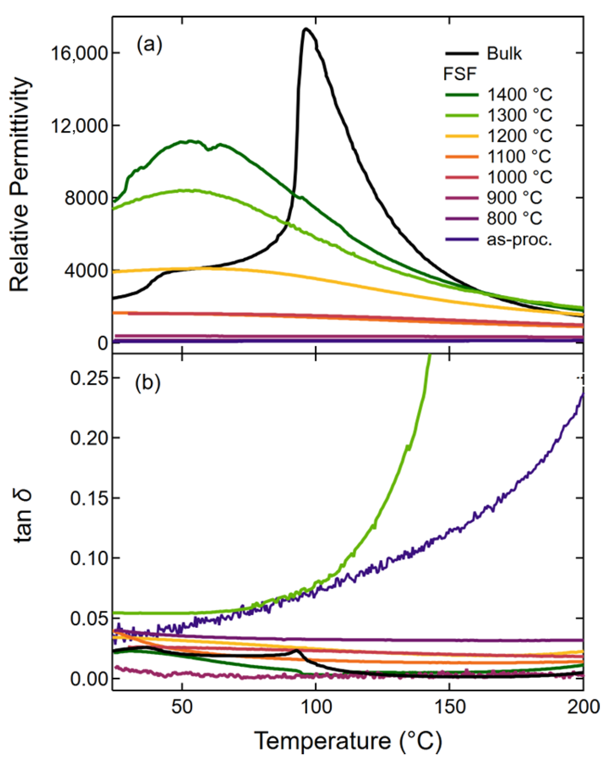
Freestanding films provide a unique opportunity to directly investigate the small and large signal responses of PAD ceramic thick films without the effects of the substrate. As such, the temperature-dependent dielectric behavior was characterized for FSFs annealed at different temperatures up to 1400 °C and compared to bulk BCZT, as shown in
Figure 9. For clarity, the relative permittivity and loss measured at 1 kHz are shown; the frequency-dependent data are provided in the
Supplementary Materials (Figure S2). Bulk BCZT displays the well-known dielectric anomalies at approximately 46 °C and 96 °C, which have been shown in previous investigations to correspond to the orthorhombic–tetragonal (
) and tetragonal–cubic (
) phase transitions, respectively [
46,
50]. In addition, anomalies in dielectric loss can also be observed in these temperature regions, consistent with structural phase transitions. The phase transitions are sensitive to the composition and are understood to be the origin of the large electromechanical response of BCZT near the polymorphic phase transition region [
51]. In contrast, the as-processed FSF shows a nearly linear dielectric response up to 200 °C, with a relative permittivity of approximately 185, due to internal residual stresses as well as a nano-grained microstructure, which significantly reduces the extrinsic contributions to the dielectric behavior. For example, Damjanovic and Demartin showed using Rayleigh behavior that the irreversible domain wall contributions to the piezoelectric response of BaTiO
3 are reduced at smaller grain sizes [
52]. This temperature-dependent behavior does not display a clear anomaly within this temperature range. In addition, the dielectric loss increases with temperature without a clear anomaly, which is due to the enhanced conductivity in as-processed films. It is important to note that the as-processed FSF displays a similar temperature-dependent dielectric response to that observed in an attached PAD film [
27], indicating that the film/substrate interactions are not responsible for the observed dielectric behavior.
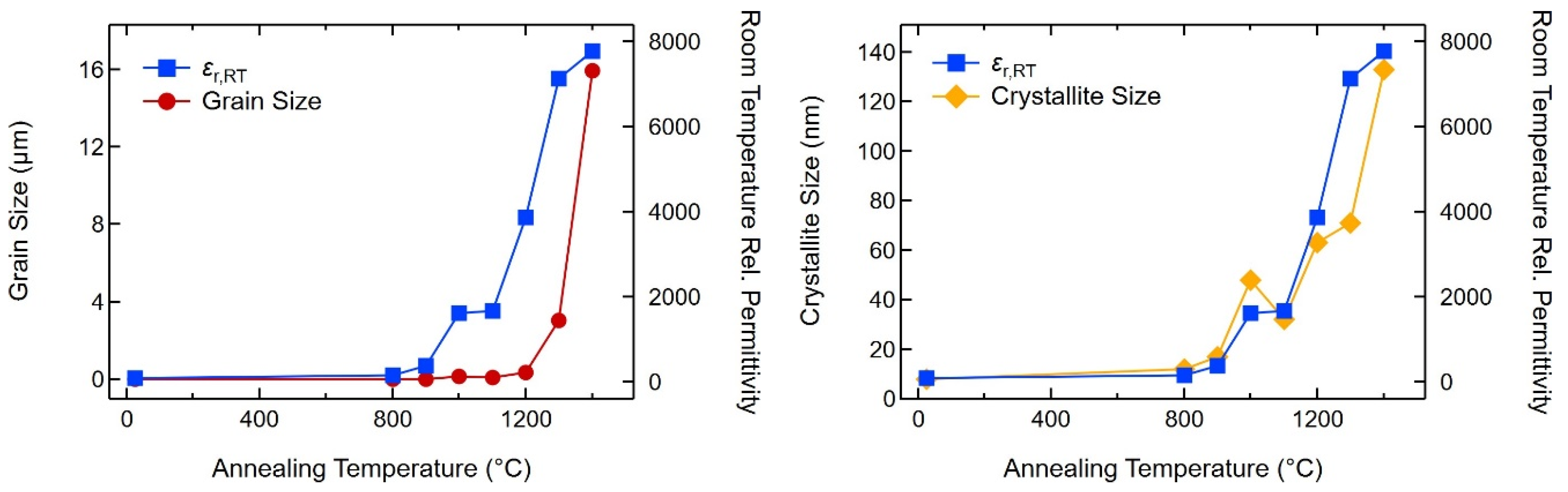
The relative permittivity of BCZT FSFs was found to increase with annealing temperature, consistent with a decrease in internal residual stress [
22,
23] and an increase in grain size (
Figure 6), leading to an improvement in the extrinsic contributions. At the lowest annealing temperature of 800 °C, there is no significant change in relative permittivity, although dielectric loss is reduced, in particular, at higher temperatures. As previously shown, 800 °C does not lead to significant grain or crystallite growth in BCZT FSFs. At 900 °C, relative permittivity increases to approximately 382. Above an annealing temperature of 900 °C, there is a more rapid increase in the room temperature permittivity value and the apparent formation of a broad maximum relative permittivity
at approximately 41–56 °C, which is lower than the known
of the bulk sample (96 °C) and approximately in the same range as its
. This corresponds very well with previous data on the grain size-dependent dielectric response as a function of temperature [
53,
54], where a similar formation of a single broad dielectric maximum was found and suggested to be due to compositional fluctuations, structural disordering, or internal stress [
54]. As can be seen in
Figure 10, the rapid increase in the room temperature relative permittivity (
) of the FSFs begins at a lower annealing temperature than the increase in grain size but corresponds with the increase in crystallite size. Previous studies have demonstrated that internal residual stress begins to decrease at lower annealing temperatures than where significant grain growth is observed [
37], suggesting that the increase in permittivity is initially due to changes in the local internal stress state. In addition, this large increase in the room temperature permittivity of FSFs annealed above 1100 °C compared to the values of the bulk sample is potentially interesting for dielectric applications.
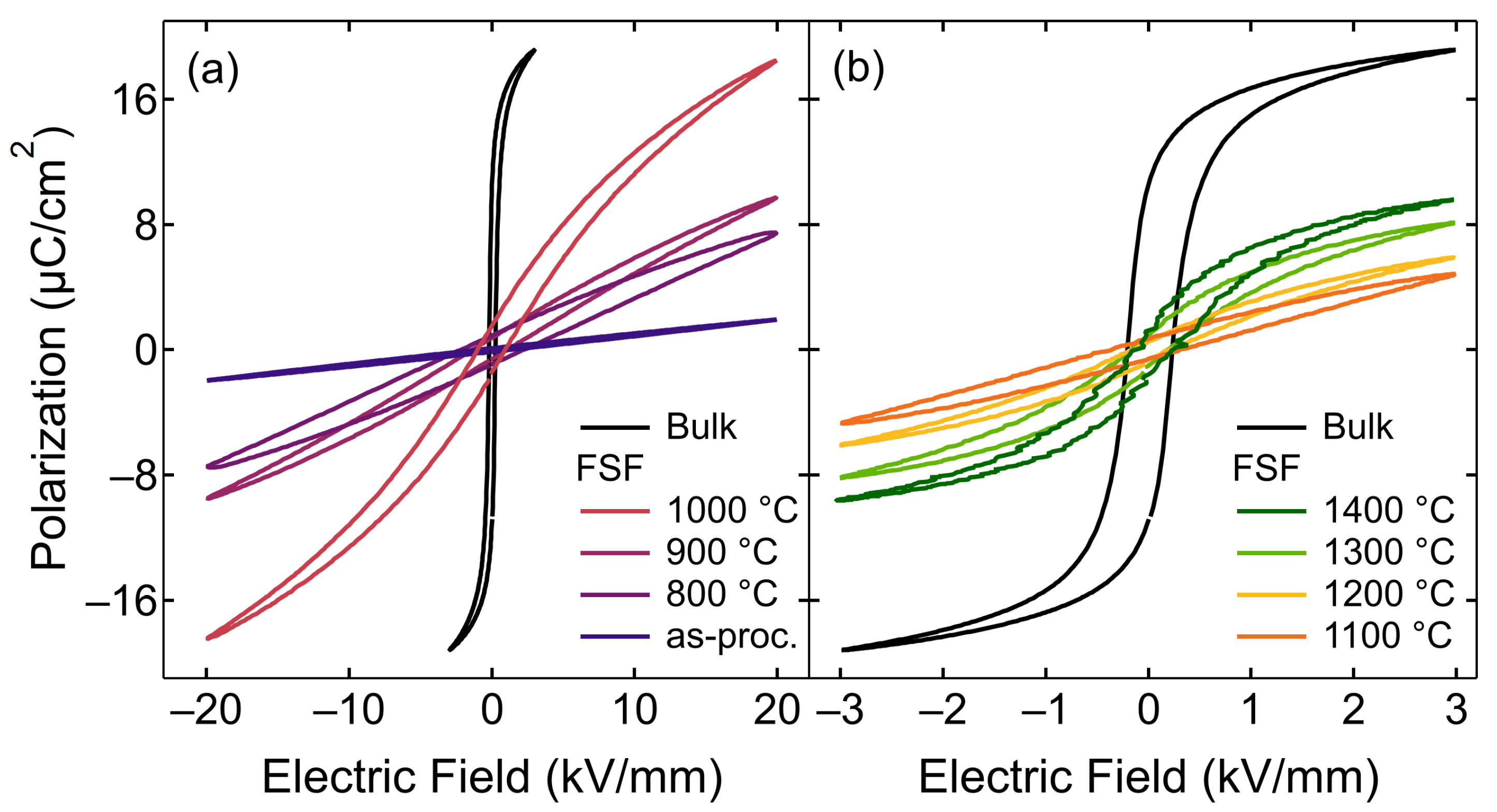
The room temperature large field polarization–electric field hysteresis was characterized for the FSFs as a function of annealing temperature as well as for the bulk sample (
Figure 11). FSFs annealed at temperatures higher than 1000 °C were characterized not higher than 3 kV/mm to avoid electric breakdown, whereas FSFs annealed at lower temperatures could be measured at higher electric fields. With increasing annealing temperature, there is an increase in the ferroelectric response, marked by an increase in the maximum polarization and a clear onset of polarization saturation at higher electric fields. In the as-processed FSF, the polarization–electric field loops appear nearly linear with limited hysteresis, consistent with a linear dielectric-like behavior. This corresponds well with the dielectric response of the as-processed FSF, which also reveals a reduced extrinsic contribution. However, despite the increase in grain size, crystallite size, and relative permittivity, assumed to be related to an increase in extrinsic contributions, the polarization–electric field behavior of the bulk sample was not reached for any FSF at 3 kV/mm. Although the reasons remain unclear, this is likely related to the mechanisms responsible for the broad dielectric maximum, where compositional fluctuations, structural disordering, or internal stress can also reduce the ferroelectric properties [
54]. In addition, internal stresses can also affect the crystal phase, as observed in nano-grained BaTiO
3 [
30]. Due to the lower volume of the FSFs, higher electric fields could be applied to samples annealed below 1100 °C, where a similar maximum polarization to the bulk sample could be achieved at 20 kV/mm. This results in a recoverable energy storage density of approximately 1.34 J/cm
3 with an efficiency of 82% at 20 kV/mm for the FSF annealed at 1000 °C, making them potentially interesting for high energy density capacitors [
55].


 ,
, 