Article

Sol–Gel Synthesis of ZnO:Li Thin Films: Impact of Annealing on Structural and Optical Properties

by
Tatyana Ivanova
1,
Antoaneta Harizanova
1,*,
Tatyana Koutzarova
2,
Benedicte Vertruyen
3 and
Raphael Closset
3
1
Central Laboratory of Solar Energy and New Energy Sources, Bulgarian Academy of Sciences, Tzarigradsko Chaussee 72, 1784 Sofia, Bulgaria
2
Institute of Electronics, Bulgarian Academy of Sciences, Tzarigradsko Chaussee 72, 1784 Sofia, Bulgaria
3
Group of Research in Energy and Environment from Materials (GREENMAT) Institute of Chemistry B6, University of Liege, B6aQuartier Agora, Allee du Six Août, 13, 4000 Liège, Belgium
*
Author to whom correspondence should be addressed.
Crystals 2024, 14(1), 6; https://doi.org/10.3390/cryst14010006 (registering DOI)
Submission received: 29 November 2023 / Revised: 15 December 2023 / Accepted: 15 December 2023 / Published: 20 December 2023

Abstract

:
A sol–gel deposition approach was applied for obtaining nanostructured Li-doped ZnO thin films. ZnO:Li films were successfully spin-coated on quartz and silicon substrates. The evolution of their structural, vibrational, and optical properties with annealing temperature (300–600 °C) was studied by X-ray diffraction (XRD), Fourier Transform Infrared (FTIR), UV-VIS spectroscopic, and field emission scanning electron microscopic (FESEM) characterization techniques. It was found that lithium doping maintains the wurtzite arrangement of ZnO, with increasing crystallite sizes when increasing the annealing temperature. Analysis of the FTIR spectra revealed a broad main absorption band (around 404 cm−1) for Li-doped films, implying the inclusion of Li into the ZnO lattice. The ZnO:Li films were transparent, with slightly decreased transmittance after the use of higher annealing temperatures. The porous network of undoped ZnO films was transformed to a denser, grained, packed structure, induced by lithium doping.

1. Introduction

Zinc oxide (ZnO) has been shown to be a remarkable material with interesting physical and chemical properties [1]. ZnO is a wideband semiconductor, possessing a direct optical band gap (Eg) of 3.37 eV at room temperature, a large exciton binding energy (60 meV), and good transparency in the visible spectral range [2]. It is known to be a non-toxic, low-cost material with high radiation hardness and high thermal conductivity, while exhibiting a strong non-linear optical behavior [3]. Due to these promising properties, ZnO materials are extensively researched for their application in optoelectronic and nanoelectronic devices [4], photocatalysis [5], piezoelectric devices [6], sensors [7], surface acoustic wave devices, as antireflection coatings and windows in solar cells [8], and as transparent electrodes [9].
Doping ZnO is a successful method for modifying and improving its electronic, chemical, optical, and morphological properties, such as modifying grains’ sizes and shapes, porosity, smoothness, etc. For example, doping ZnO with trivalent donor dopants such as Al3+, Ga3+, and In3+ on Zn2+ sites typically results in improved n-type conductivity [10]; meanwhile, p-type ZnO can be achieved by introducing nitrogen (N), phosphorus (P), arsenic (As), antimony (Sb), and lithium (Li) dopants [11]. The ZnO band gap can be tailored by doping with such materials as Mg [12]. Rare-earth metal doping of ZnO is reported to be an effective way for the adjustment and control of gas-sensing efficiency [13]. Generally, doping alters the ZnO-based materials in view of different applications by enhancing the desired properties through choosing the appropriate dopant.
Lithium-doped ZnO structures are interesting for scientific research, as Li doping can induce enhanced optical, electrical, magnetic, and photoluminescence properties [14]. ZnO:Li has been reported to exhibit improved crystal quality, high sensitivity as a UV sensor [15], piezoelectric response [16], p-type conductivity [17], etc. The evident photocatalytic properties of ZnO:Li have also been reported [18].
Undoped ZnO films exhibit n-type conductivity as a consequence of deviation from their stoichiometry and of the presence of native donor defects, such as zinc interstitial (Zni) and oxygen vacancy (V0) [19]. For different applications, such as p–n junction-based devices or bipolar device applications, it is necessary to obtain stable p-type oxide semiconductors [19,20]. There are two ways of inducing p-type conductivity in ZnO: one is doping with group I elements (Li, Na, K) at the Zn site; the other is substitution at the O site by group V elements (N, P, Sb) [19]. Lithium is a prospective dopant candidate, as it possesses a small ionic radius (0.68 Å) that is very close to the ionic radius of Zn (0.74 Å) [21,22]. Experimentally, it has been shown that Li doping provokes p-type semiconductivity by creating deep acceptor levels due to the Li atoms occupying Zn sites in the wurtzite host lattice and the Li1+ ions acting as shallow acceptors [14]. On the other hand, Li1+ ions can also occupy the interstitial positions (Lii), where they become electron donors [23,24].
ZnO:Li films have been fabricated by numerous deposition techniques, including pulsed laser deposition [25], spray pyrolysis [26], sol–gel [15], electron beam evaporation [27], magnetron sputtering [28], etc. The sol–gel method exhibits several advantages, such as control of the film composition, easy film fabrication on large-area substrates, and low cost [29,30].
In this work, we present the sol–gel deposition of Li-doped ZnO thin films. ZnO:Li films were obtained by the spin-coating method on quartz and silicon substrates. The prepared sol solutions (Zn and mixed Zn/Li sols) remained stable for a period of five months, which is a very good technological achievement. In addition, a detailed study of the properties covering a wide temperature range, from 300 to 600 °C, is performed. The obtained samples are structurally characterized using XRD analysis and FTIR spectroscopy. Their optical properties are analyzed using UV-VIS spectroscopy in the spectral range of 240–1800 nm. The change in the optical band gap and refractive index with annealing is discussed. The influence of a lithium dopant on the ZnO film morphology is revealed.

2. Materials and Methods

A sol–gel spin-coating approach was applied to preparing ZnO and ZnO:Li thin films. A 0.4 M Zn sol solution was prepared: First, zinc acetate dihydrate Zn(CH3COO)2·2H2O (Riedel de Haen, Hannover, Germany) was dissolved in absolute ethanol (Merck KgaA Darmstadt, Germany, absolute for analysis) [31]. Secondly, monoethanolamine (MEA, Fluka AG, Buchs, Switzerland, 98%) was added to bring the MEA/Zn molar ratio to unity. Finally, lithium nitrate LiNO3 (Sigma-Aldrich Chemie GmbH, Taufkirchen, Germany) was added to reach a 0.04:1 Li:Zn molar ratio. Then, the solution was stirred using a magnetic stirrer (MS-H280-PRO, DLAB Scientific Co., Ltd., Beijing, China) at 55 °C for 1 h, followed by treatment in an ultrasonic cleaner (ELMA Elmasonic Easy 10H, Elma Schmidbauer GmbH, Singen, Germany) at 45 °C for 2 h. The obtained sols (pure and mixed solutions) were transparent with no precipitations. They were stable for a period of 5 months.
ZnO and ZnO:Li films were deposited on cleaned substrates by spin-coating (spin coater P 6708, PI-KEM Limited, Staffordshire, UK) at a 4000-rpm rotational speed for 30 s. The substrate cleaning included the following steps: cleaning in acetone, then treatment in ethanol (both steps were performed in an ultrasonic bath at 45 and 60 °C, respectively), and rinsing in double-distilled water. The final films were obtained after repeating the spin-coating process five times and, after each cycle of spin-coating, the substrates were preheated at a temperature of 300 °C for 10 min in a chamber furnace (chamber furnace, Tokmet—TK Ltd., Varna, Bulgaria) to evaporate the solvent and to decompose and remove the organic compounds. The sol–gel ZnO and ZnO:Li films were annealed at 300, 400, 500 and 600 °C for 1 h in air. Si wafers (FZ, p-type, resistivity 4.5–7.5 Ω, orientation ˂100˃) were used for XRD, FESEM and FTIR studies, and UV-graded quartz-glass substrates (thickness 1 mm ± 0.1), for optical measurements.
The films’ thickness was measured using an LEF 3 M laser ellipsometer (Siberian Branch of the Russian Academy of Sciences, Novosibirsk) with a He-Ne laser at the wavelength of 632.8 nm. The films’ thickness values were 160 and 165 nm for ZnO and ZnO:Li films, respectively. These values were close so that the comparison of the films’ optical and structural properties was appropriate.
The FTIR spectra were taken by an IR Prestige-21 FTIR spectrophotometer (Shimadzu Corporation, Kyoto, Japan) in the spectral range 350–4000 cm−1 (resolution of 4 cm−1) using a bare Si wafer as background. The X-ray diffraction patterns were recorded by a Bruker D8 XRD diffractometer (Bruker AXS GmbH, Karlsruhe, Germany) using a Cu anode (Kα radiation) at a grazing angle of 1°, a step time of 2 s and a step of 0.04°. The optical spectra were recorded using a Shimadzu 3600 UV–VIS–NIR double-beam spectrophotometer (Shimadzu Corporation, Kyoto, Japan) in the 240–1800 nm spectral range and at a resolution of 0.1 nm. The transmittance was measured against air. The reflectance spectra were taken by using the specular reflectance accessory (at a 5° incidence angle) with an Al-coated mirror as reference. A four-point probe (model FPP-100, Veeco Instruments Inc.) was used for determining the samples’ sheet resistance.
The films’ morphologies were studied by field emission scanning electron (FESEM) microscopy (Philips XL 30FEG-ESEM, FEI, FEI Europe B.V., Zaventem, Belgium). A Au coating was deposited over the samples’ surfaces before the measurements.

3. Results and Discussions

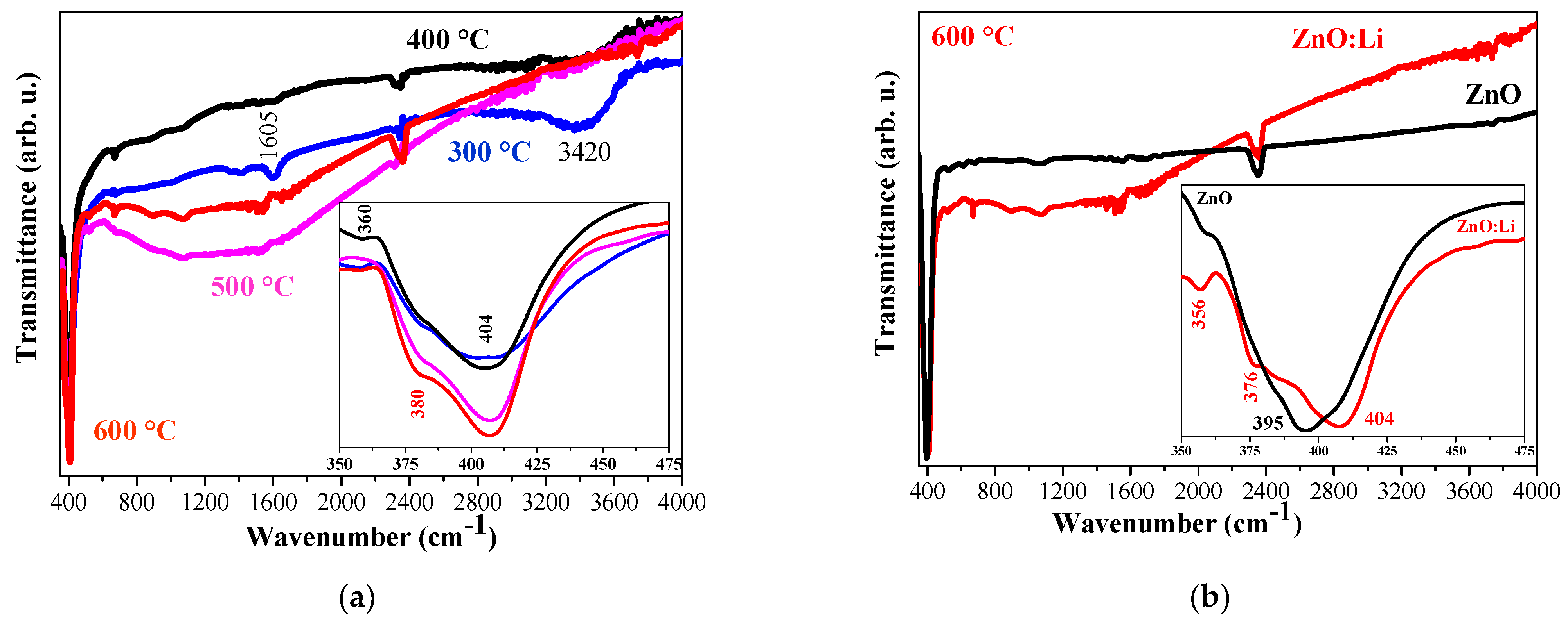
3.1. FTIR Investigation

FTIR spectroscopy is a technique used for identification of chemical bonds and functional groups [14]. The shapes and intensities of the absorption features depend on the sample’s crystallinity, chemical composition, impurities, stress, and morphology, as well as on the crystallite’s size and shape [32]. Figure 1a presents FTIR spectra of ZnO:Li films annealed at different temperatures; Figure 1b shows a comparison of the spectra of a ZnO and a ZnO:Li film after annealing at the highest temperature (600 °C). Introducing a dopant into the ZnO lattice can change the characteristic IR lines and give rise to new bands.
The ZnO:Li film treated at 300 °C showed a strong and broad band at 3420 cm−1, which was assigned to the stretching modes of hydroxyl groups. The corresponding OH bending vibrations were manifested by the characteristic line at 1605 cm−1 [14].
The hydroxyl groups’ absorption bands vanished as the annealing temperature was increased, and the two IR lines at 3420 and 1605 cm−1 disappeared after the 500 °C thermal treatment. The absorption lines at 2346 and 2378 cm−1 observed in the spectra were related to CO2 since the FTIR spectra were recorded in air [33]. The hydroxyl absorption bands were absent in the undoped ZnO spectra, even for the sample treated at the lowest annealing temperature (300 °C).
The characteristic metal-oxide absorption bands arising from inter-atomic vibrations generally appeared in the fingerprint IR region, i.e., below 1000 cm−1 [34]. The main absorption band of ZnO:Li films was observed at 404 cm−1; its intensity rose with the annealing temperature (as can be seen in the inset in Figure 1a). This band was associated with the stretching Zn–O vibrations [34,35].
The comparison between the undoped and doped samples (Figure 1b) revealed that Li doping shifted the strongest IR line from 395 to 404 cm−1. The absorption band of the ZnO:Li sample had an asymmetrical shape and a clear feature at 376 cm−1. Another peak at 356 cm−1 was also seen. These lines were attributed to Zn-O stretching vibrations [32]. For all of the annealing temperatures, the main band of the Li-containing ZnO films was wider, proving that the Li ions were embedded into the host lattice [33].
The FTIR study revealed that adding Li was manifested by changes in the absorption features. Raising the annealing temperatures led to stronger IR lines, suggesting that the film crystallinity was improved. XRD analysis was applied for revealing the crystallinity evolution with annealing.

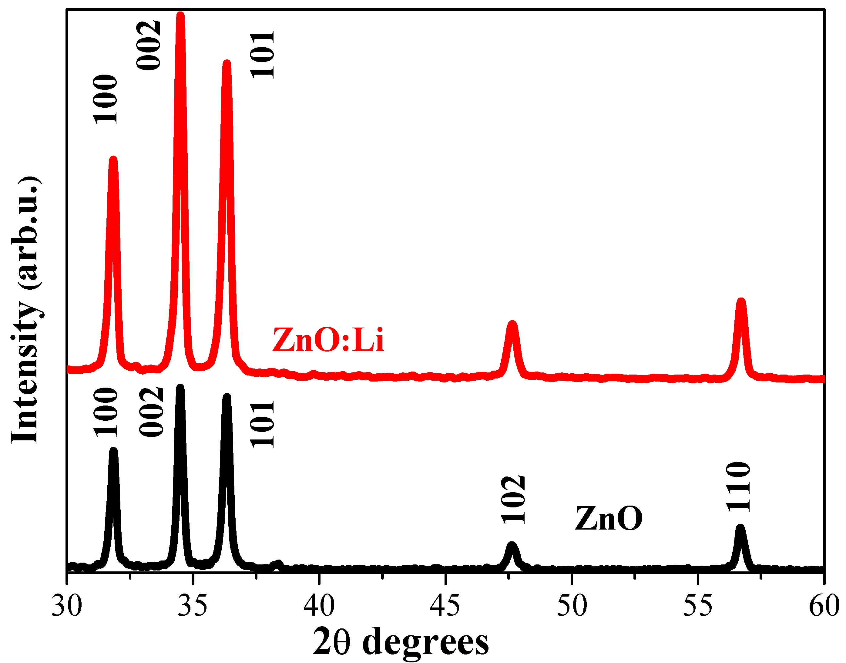
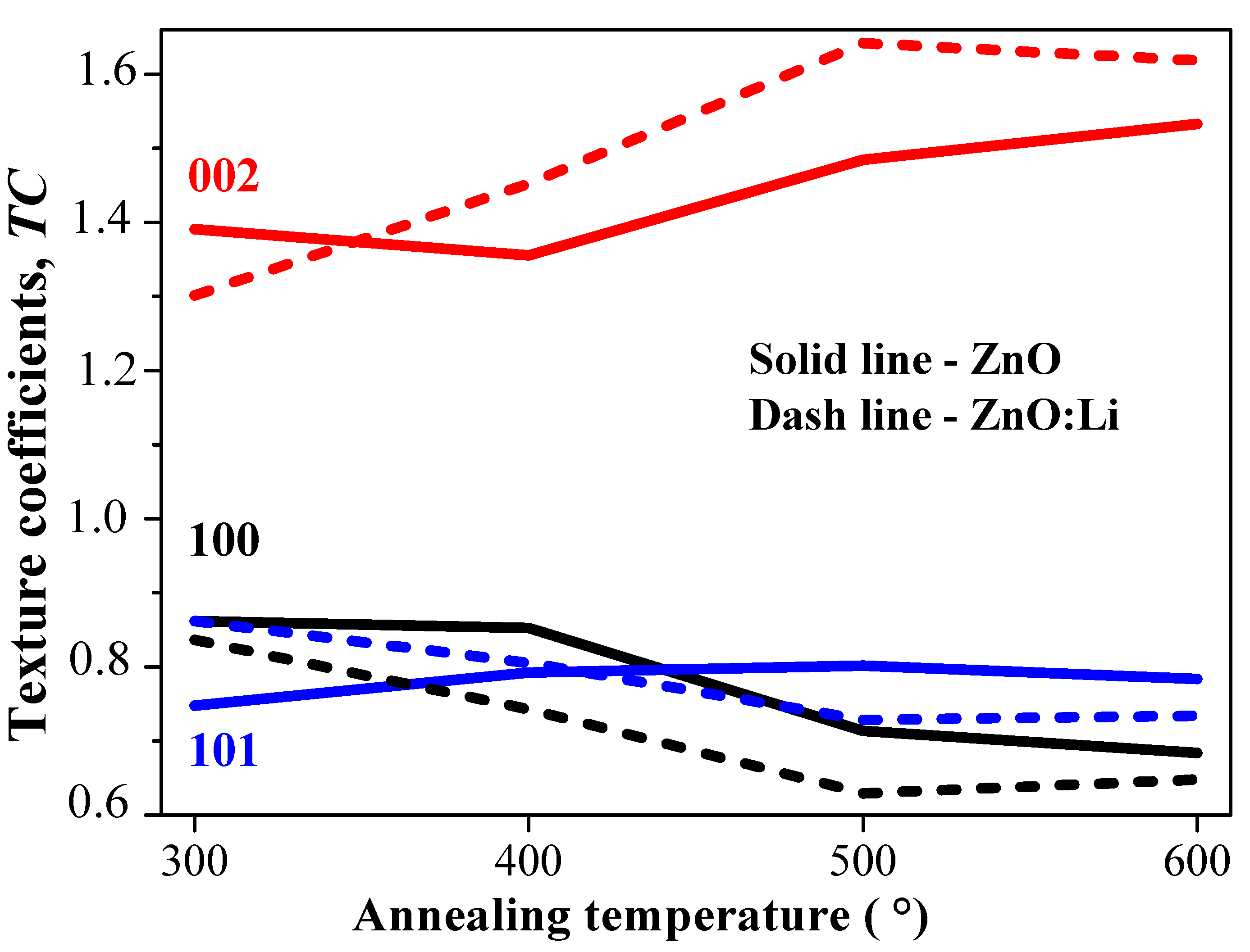
3.2. XRD Structural Study

Figure 2 presents the XRD patterns of Li-doped ZnO films deposited on Si substrates; the XRD patterns of undoped ZnO and ZnO:Li films annealed at 600 °C are shown in Figure 3. The X-ray diffraction patterns matched well with the standard values of hexagonal wurtzite ZnO (JCPDS PDF card no. 00-036-1451) and confirmed the sol–gel films’ crystallization. The structural results revealed the polycrystalline nature of all samples.
All peaks observed could be indexed to zinc oxide. No diffraction peaks related to Li-containing phases were detected; this may suggest the incorporation of lithium in the ZnO crystal structure, but the low Li concentration could also be responsible for the absence of a signature in the XRD patterns.
Table 1 summarizes the ZnO lattice parameters, the crystallite size, the dislocation density and the c/a ratio of undoped ZnO and ZnO:Li films. These parameters were determined using the equations given in [36,37]. The crystallites’ average size (d) was estimated by the Scherrer equation [37] using the full width at half maximum (FWHM) of the (100), (002) and (101) diffraction peaks. In order to allow a comparison with reference data, we also quoted 1/d2, which many authors call the dislocation density [36], although this formula is a simplification of Williamson and Smallman’s work on annealed and cold-worked metals [38].
Increasing the annealing temperature induced an increase in the crystallite size in both cases. The differences in the crystallite size between undoped and Li-doped ZnO were too small to draw conclusions, although the fact that the crystallite size was somewhat larger for undoped ZnO at 600 °C agrees with the trend observed by Fujihara et al. [30] for the sol–gel films.
As noted above, both undoped ZnO and ZnO:Li films crystallized in a wurtzite phase. The wurtzite structure had a hexagonal unit cell with two lattice parameters, a and c, in the ratio of c/a = 1.633 (an ideal wurtzite crystal) and belonged to the P63mc space group. In a real ZnO crystal, the wurtzite structure deviates from the ideal arrangement—the c/a ratio is close to 1.60. Many factors have been reported to affect the lattice parameters and the c/a ratio: (i) lattice distortion, (ii) impurities and defects (iii) differences in the ionic radii of O2−, Zn2+, and Li+, (iv) external strains induced by the substrate and the temperature, (v) electrostatic interactions between the ions in the lattice (these interactions influence the optimal distances between the ions in undoped and doped zinc oxide) [39], and (vi) defects in the real lattice [40]. However, in the present case, the lattice parameter variations caused by Li doping and thermal treatment were not significant given the uncertainty in the peak positions. Indeed, the percentage of lithium was rather small. Hjiri et al. [41] also did not observe any (002) peak shifts for Li doping concentrations up to 3 at%. Both Song et al. [16] and Jeong et al. [28] reported a small decrease in the c parameter in the case of a Li-doped film prepared by magnetron sputtering, a technique allowing one to reach higher levels of lithium trapped in the ZnO matrix in comparison with the sol–gel routes. The c/a ratio values of sol–gel ZnO and ZnO:Li films differed slightly from the reference value of 1.602 of ZnO (PDF card no. 00-036-1451). A more significant effect of Li addition was observed regarding the intensity distribution between the (100), (002) and (101) peaks illustrated in Figure 4 as the texture coefficient (TC) calculated from the following equation [42]:
T C   h k l = I ( h k l ) I o ( h k l ) N 1 N I ( h k l ) I o ( h k l )
where I(hkl) is the measured relative intensity; Io(hkl) is the (hkl) plane standard intensity; and N is the number of diffraction lines. The standard intensities for (100), (002) and (101) were taken from PDFS card 01-070-8070. Considering the small 2θ range for these three reflections, combining the experimental intensities collected in grazing incidence with the standard intensities in a Bragg–Brentano geometry did not affect the qualitative conclusions.
Figure 4 presents the annealing temperature effect on the estimated texture coefficients (TC) of the (100), (002), (101) diffraction planes. It is known that the TC value represents the texture of the particular plane—its exceeding unity implies a preferred crystallite growth with this orientation. The ZnO and ZnO:Li films considered here both had TC (101) and TC (100) below unity, which indicates that the preferred orientation was along another direction. The TC (100) values were near 0.8 for ZnO and in the range 0.73–0.86 for ZnO:Li (Figure 4). TC (002) was greater than unity for both undoped (1.36–1.53) and Li-doped ZnO (1.30–1.64). Thus, it was found that Li doping brings about a higher degree of orientation along the 002 plane for annealing temperatures in the 400–600 °C range. The highest value of 1.64 was measured for the ZnO:Li film treated at 500 °C.
The XRD studies showed that Li doping had a slight impact on the wurtzite structure of the ZnO films. The sol–gel ZnO:Li films crystallized with a preferential growth orientation along the c-axis. The hexagonal wurtzite structure was maintained without the formation of an additional phase. The small Li doping level did not modify significantly the lattice parameters and the crystallite size, while the thermal treatment favored the growth of larger crystallites.

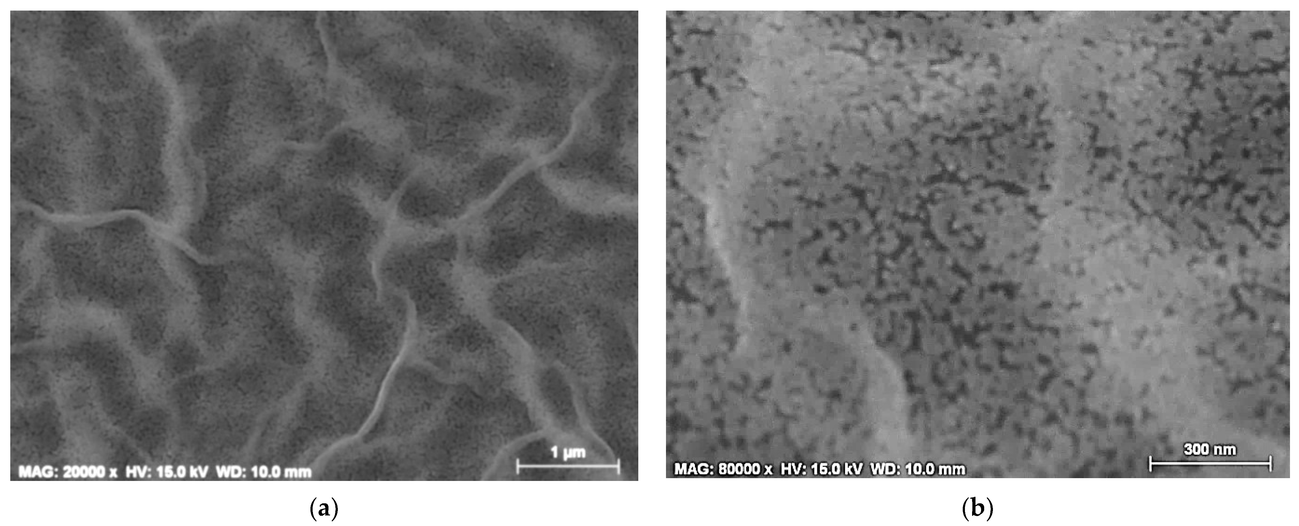
3.3. Film Surface Morphology

The ZnO:Li surface morphology evolution with the annealing was studied by FESEM. The samples were deposited on Si wafers and treated at 300 and 600 °C. Figure 5 shows the FESEM images (at two magnifications) of the sol–gel Li-doped ZnO film annealed at 300 °C. The surface morphology has a wrinkle-type surface structure with thinner and thicker wrinkles (at the magnification of 20,000, Figure 5a). The formation of wrinkles on the surface of sol–gel ZnO coatings was reported previously in [43,44]. Some authors [45] proposed that voids appear as a result of elimination of residual organic solvents during the preheating and annealing procedures, so that the stress imbalance arising in the films causes wrinkle-like surface features [46].
The image at higher magnification (Figure 5b) illustrates a rather porous structure with tiny grains with sizes below 20 nm that are difficult to distinguish. The average crystallites size determined by XRD was 11 nm, as estimated from the diffraction planes (112), (103), (110), (101), (002) and (100). The FESEM study revealed similar or slightly bigger grains; however, as known, the crystallite size is assumed to be the size of a coherently diffracting domain and does not represent exactly the particle size [40].
The annealing at 600 °C produced different morphologies. A comparison of the FESEM images of undoped ZnO and ZnO:Li films obtained under the same technological conditions is given in Figure 6. The lithium dopant provoked a significant change in the film morphology. The undoped ZnO film exhibits wrinkles with a very porous structure, with the grains having irregular shapes in sizes varying from 30 to 100 nm (Figure 6a,b). Annealing the sol–gel ZnO:Li film at the highest temperature resulted in a wrinkle-type surface structure (Figure 6c) with well-defined fibers (or wrinkles) consisting of distinct nanoparticles (Figure 6c). The grains of the ZnO:Li thin film annealed at 600 °C clung closely to each other. The highest annealing temperature transformed the porous film morphology to a denser structure without pores and with well-defined grains, some of which were of spheroidal shape. The grain size (as determined from the micrograph with 80,000 magnification, Figure 6d) varied from 30 nm to 110 nm.
The morphology of undoped ZnO is porous, while the ZnO:Li films manifest a denser structure with closely packed grains. The FESEM images confirmed that the ZnO:Li films are nanostructured materials, with the thermal treatment causing structural and surface modifications of the films.

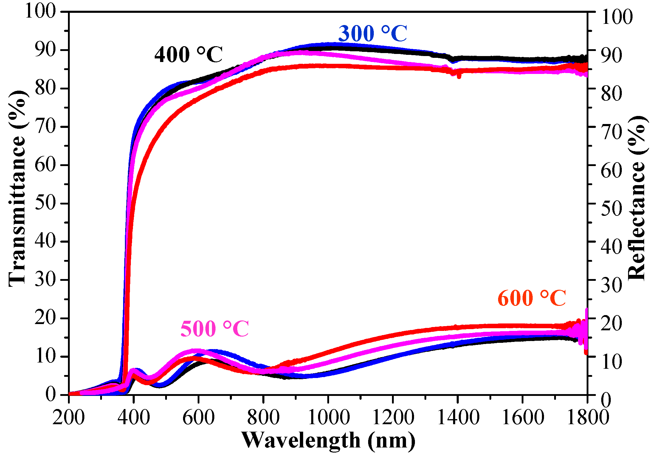
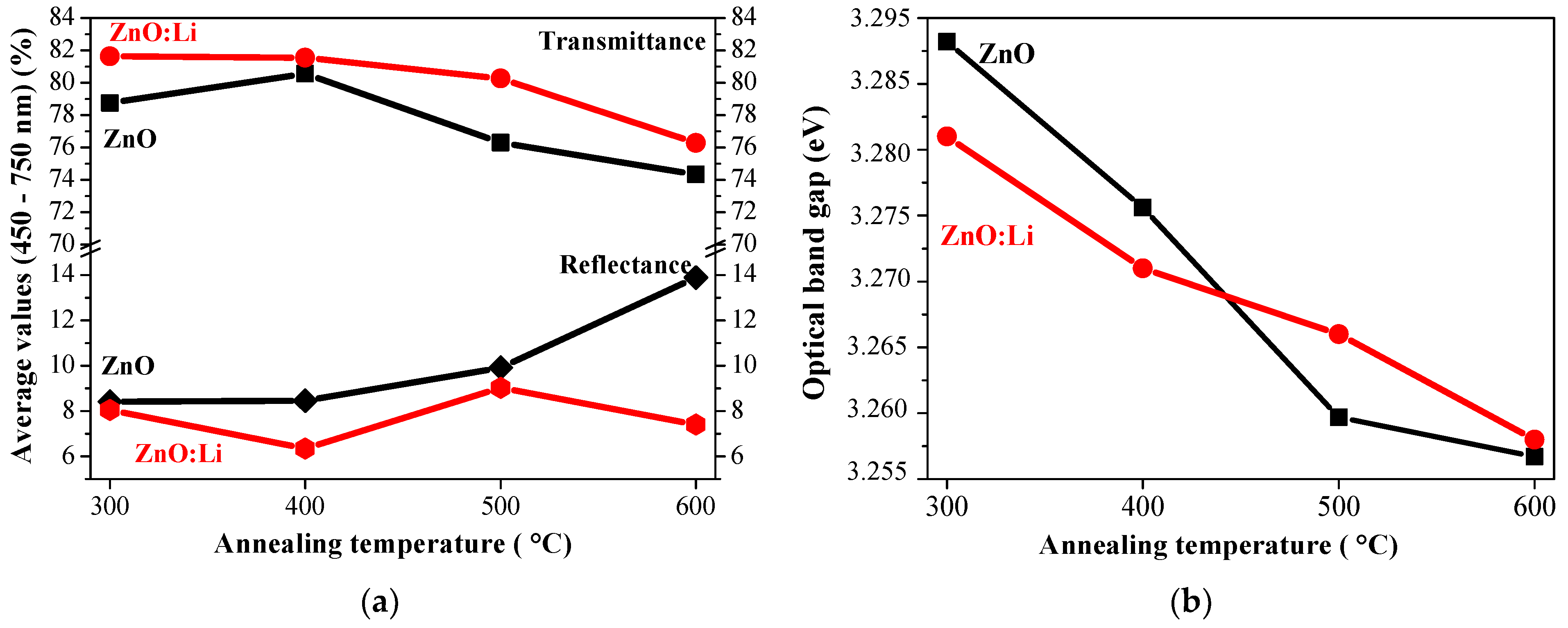
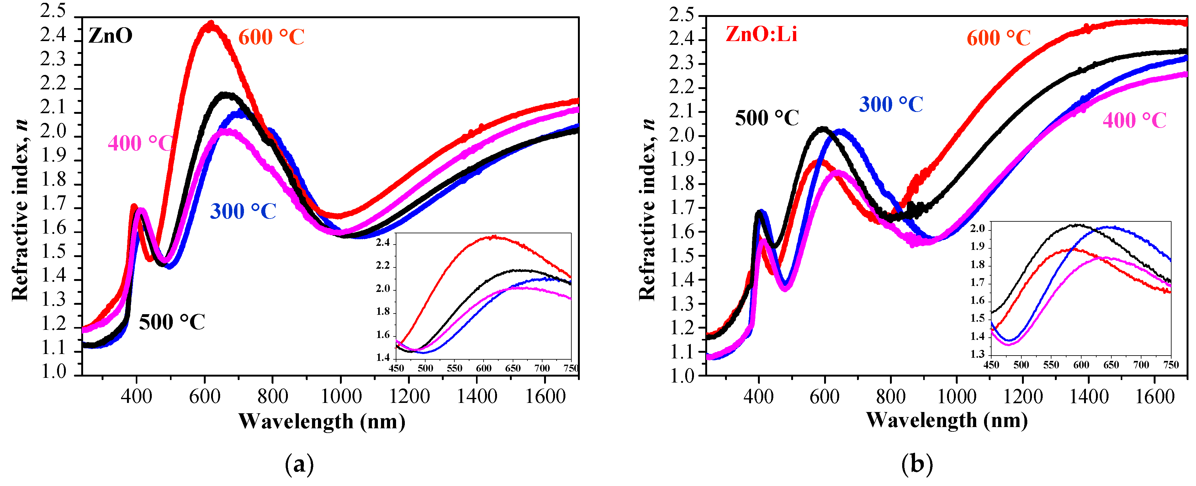
3.4. Optical Characterization

Figure 7 presents the spectra of ZnO:Li thin films annealed from 300 to 600 °C and recorded in the 200–1800 nm spectral range. The thermal treatment reduced slightly the films’ transparency. The difference appeared after the annealing at 600 °C. The ZnO:Li films annealed at temperatures above 400 °C showed exciton absorption peaks around 340 nm, confirming the good crystallinity of the films [46]. Figure 8a provides the average values of the transmittance and reflectance in the visible spectral region (450–750 nm) of undoped and Li-doped ZnO films. Following the post-annealing, the average optical transmittance slightly decreased. The average reflectance was below 9% and changed weakly with the annealing temperature. The average transmittance and reflectance of the bare quartz substrate were 93.5% and 6.7%, respectively. The Li doping improved the optical transparency. The ZnO:Li films’ reflectance was lower than that of the ZnO films. The undoped films exhibited a trend of increasing the reflectance at higher annealing temperatures. The FESEM analysis and the microscopic images revealed denser and smoother surfaces of the sol–gel doped films. The smooth morphology resulted in an improved average transmittance of the Li-doped ZnO films.
The optical band gap is derived from the first derivative of the transmittance versus the energy [47]. The estimated optical band gap (Eg) values for ZnO and ZnO:Li films are shown in Figure 8b as a function of the annealing temperatures; the results are in good agreement with the literature data for ZnO-based materials [48,49]. A narrowing trend was seen in the Eg of the ZnO and ZnO:Li films annealed at the higher temperatures. The optical band gap can be influenced by several factors, including crystallization, grain sizes, structural parameters, impurities, etc. [50]. The decrease in the band gap energy with annealing correlated with the growth of crystallites of greater size [50].
The lower values of the optical band gap of ZnO:Li films compared to undoped ZnO after annealing at 300 and 400 °C can be related to the change in the lattice parameters and the formation of a tail band [51]. The higher-temperature thermal treatments (at 500 and 600 °C) reversed this tendency, as ZnO:Li samples have wider optical band gaps than those of ZnO (Figure 8b). The widening of Eg can be due to the Burstein–Moss effect and to Li occupying interstitial sites in ZnO [51].
The refractive index, n, is an important parameter characterizing the optical properties of a thin film. The refractive index for the wavelengths ranging from 240 to 1700 nm was calculated using the measured reflectance spectra of the ZnO and ZnO:Li films. The following relation was used [52]:
R = ( n 1 ) 2 + k 2 ( n + 1 ) 2 + k 2
where k is the extinction coefficient and R is the reflectance. If k << n, then:
n = 1 + R 1 R
Figure 9 displays the obtained values for the refractive index of undoped ZnO (Figure 9a) and ZnO:Li (Figure 9b) films annealed at 300–600 °C.
The values of n depend strongly on the wavelength. The wavelengths of the undoped ZnO films revealed that n increases as the annealing temperature is increased, especially in the visible spectral range (Figure 9a). A similar tendency was observed for the ZnO:Li films in the near IR region above 1000 nm. For wavelengths below 750 nm, the refractive index of the doped samples treated at 300 and 500 °C reached its highest values. Generally, the refractive index of the ZnO:Li is lower than that of the ZnO films in the wavelength region 240–990 nm. In the NIR spectral range, the ZnO:Li films’ n values exceeded those of ZnO. The decrease in the refractive index with Li doping in the range 300–900 nm has been reported by other authors [53]. In contrast, other researchers [50,54] reported higher refractive index values for Li-doped ZnO films. The refractive index of single-crystal ZnO is 2.047–2.063 at 500 nm [55]. The obtained n values are in agreement with the reported values. It must be noted that there is a large dispersion in the reported values of the refractive index of ZnO-based materials depending on the deposition methods, the technological conditions, stoichiometry, crystallinity, dopants and packing density [55].
The optical characterization of the studied ZnO:Li films demonstrated an improved transparency (up to 82%) and a change in the optical band gap (a narrowing from 3.281 to 3.258 eV with the temperature). The refractive index reduction in the visible spectral range was caused by incorporation of Li in the zinc oxide host lattice.

3.5. Electrical Properties

The transparent conductive films’ performance can be evaluated by using the concept of the figure of merit (FOM) (Haacke [56]) and Equation (4):
F O M = T a v e r a g e 10 R s h e e t
where Taverage is the average transmittance in a certain spectral region (in our case, 450–750 nm) and Rsheet is the sheet resistance of the samples. The FOM yields a numerical value derived from the two most important parameters of a transparent conductor, namely, transmittance and sheet resistance. It is known that these parameters in semiconductors are interdependent—this is why the figure of merit is used [57]. Improving the optical transparency (or electrical conduction) will result in a reduction in the electrical conduction (or transmittance) [57].
Table 2 presents the FOM values estimated for the sol–gel Li-doped ZnO films treated at 300, 500 and 600 °C. The values quoted for the average transmittance were evaluated in the visible spectral range 450–750 nm by extracting the quartz substrate transmittance. The sheet resistance was measured using the four-probe technique.
In order to highlight the effect of the sol–gel method on the FOM of the ZnO thin films, a comparison of the properties of thin films with similar doping in terms of dopant and doping level is necessary. Unfortunately, to the best of our knowledge, data on Li-doped ZnO thin films are not available. Table 3 presents a comparison of reported sheet resistance and FOM values for ZnO-based films prepared by different deposition methods [43,58,59,60,61,62]. As can be seen, the Rsheet and FOM values vary widely. Comparing the results of the sol–gel ZnO:Li films studied in the present work, it is seen that they approached the reported values, but there are doped and undoped ZnO films with better electrical properties. It must be emphasized that this study was focused on the effects of Li doping and the annealing temperatures on the structural, optical and morphological properties of ZnO films.
Regarding the electrical properties of sol–gel ZnO:Li films, further research is needed on optimizing the preheating and post-annealing procedures and the films’ thickness and transparency. In this respect, the results obtained in the present work are promising.

4. Conclusions

Thin films of lithium-doped zinc oxide were successfully prepared on Si and quartz substrates using the simple sol–gel spin-coating method. The FTIR analysis showed that including Li in ZnO thin films markedly modified and shifted the absorption bands. No absorption bands related to Li oxides were detected. The XRD patterns demonstrated the polycrystalline structure of the ZnO:Li films, which kept their wurtzite structure; no Li-containing crystalline phases were detected. The crystallite sizes increased as the annealing temperature was increased, and doping with lithium changed the temperature evolution of the texture coefficients (TC) in ZnO. The preferential (002) orientation was enhanced in the ZnO:Li films compared to the undoped samples. Introducing the dopant annealing modified the surface morphology. The FESEM observations showed a more uniform and compact structure of the ZnO:Li films, which were composed of closely packed spherical nanograins, in contrast to the very porous structure of the undoped ZnO consisting of randomly distributed irregular grains. The Li dopant improved the ZnO optical transparency across the visible spectral range, as the average transmittance was found to be higher than 80% for the ZnO:Li films annealed at 300–500 °C. The preliminary electrical study yielded encouraging results. In summary, we can conclude that lithium doping affects the structural, optical and morphological properties of sol–gel prepared ZnO thin films. Further, the ZnO:Li nanostructured thin films deposited using the cost-effective sol–gel process are promising candidates for practical technological applications.

Author Contributions

Conceptualization, T.I. and A.H.; methodology, T.I., A.H., T.K. and B.V.; validation, T.I. and R.C.; formal analysis, T.I., T.K. and A.H.; investigation, T.I., A.H., T.K., B.V. and R.C.; data curation, T.I., T.K. and B.V.; writing—original draft preparation, T.I., A.H., T.K. and B.V.; writing—review and editing, T.I.; visualization, T.K. and R.C.; supervision, T.I.; project administration, T.I. All authors have read and agreed to the published version of the manuscript.

Funding

This research received no external funding.

Data Availability Statement

Data are contained within the article.

Conflicts of Interest

The authors declare no conflict of interest.

References

  1. Morales, C.; Leinen, D.; del Campo, A.; Ares, J.R.; Sanchez, C.; Flege, J.I.; Gutierrez, A.; Prieto, P.; Soriano, L. Growth and characterization of ZnO thin films at low temperatures: From room temperature to −120 °C. J. Alloys Comp. 2021, 884, 161056. [Google Scholar] [CrossRef]
  2. Wang, Z.; Luo, C.; Anwand, W.; Wagner, A.; Butterling, M.; Rahman, M.A.; Phillips, M.R.; Ton-That, C.; Younas, M.; Su, S.; et al. Vacancy cluster in ZnO films grown by pulsed laser deposition. Sci. Rep. 2019, 9, 3534. [Google Scholar] [CrossRef] [PubMed]
  3. Borysiewicz, M.A. ZnO as a Functional Material, a Review. Crystals 2019, 9, 505. [Google Scholar] [CrossRef]
  4. Muchuweni, E.; Sathiaraj, T.S.; Nyakotyo, H. Synthesis and characterization of zinc oxide thin films for optoelectronic applications. Heliyon 2017, 3, e00285. [Google Scholar] [CrossRef] [PubMed]
  5. Mohamed, K.M.; Benitto, J.J.; Vijaya, J.J.; Bououdina, M. Recent Advances in ZnO-Based Nanostructures for the Photocatalytic Degradation of Hazardous, Non-Biodegradable Medicines. Crystals 2023, 13, 329. [Google Scholar] [CrossRef]
  6. Pandey, K.; Dutta, J.; Brahma, S.; Rao, B.; Liu, C.P. Review on ZnO-based piezotronics and piezoelectric nanogenerators: Aspects of piezopotential and screening effect. J. Phys. Mater. 2021, 4, 044011. [Google Scholar] [CrossRef]
  7. Khatibani, A.B. Characterization and Ethanol Sensing Performance of Sol-Gel Derived Pure and Doped Zinc Oxide Thin Films. J. Electron. Mater. 2019, 48, 3784–3793. [Google Scholar] [CrossRef]
  8. Wibowo, A.; Marsudi, M.A.; Amal, M.I.; Ananda, M.B.; Stephanie, R.; Ardy, H.; Diguna, L.J. ZnO nanostructured materials for emerging solar cell applications. RSC Adv. 2010, 10, 42838–42859. [Google Scholar] [CrossRef]
  9. Hála, M.; Fujii, S.; Redinger, A.; Inoue, Y.; Rey, G.; Thevenin, M.; Deprédurand, V.; Weiss, T.P.; Bertram, T.; Siebentritt, S. Highly conductive ZnO films with high near infrared transparency. Prog. Photovolt. Res. Appl. 2015, 23, 1630–1641. [Google Scholar] [CrossRef]
  10. Zhao, D.; Li, J.; Sathasivam, S.; Carmalt, C.J. n-Type conducting P doped ZnO thin films via chemical vapor deposition. RSC Adv. 2020, 10, 34527–34533. [Google Scholar] [CrossRef]
  11. Pathak, T.K.; Kumar, V.; Swart, H.C.; Purohit, L.P. P-type conductivity in doped and codoped ZnO thin films synthesized by RF magnetron sputtering. J. Modern Opt. 2015, 62, 1368–1373. [Google Scholar] [CrossRef]
  12. Mia, M.N.H.; Mia, M.F.; Pervez, M.F.; Khalid Hossain, M.K.; Rahman, M.R.; Uddin, M.J.; Al Mashud, M.A.; Ghosh, H.K.; Hoq, M. Influence of Mg content on tailoring optical bandgap of Mg-doped ZnO thin film prepared by sol-gel method. Results Phys. 2017, 7, 2683–2691. [Google Scholar] [CrossRef]
  13. Sayago, I.; Santos, J.P.; Sánchez-Vicente, C. The Effect of Rare Earths on the Response of Photo UV-Activate ZnO Gas Sensors. Sensors 2022, 22, 8150. [Google Scholar] [CrossRef] [PubMed]
  14. Punia, K.; Lal, G.; Dolia, S.N.; Kumar, S. Defects and oxygen vacancies tailored structural, optical, photoluminescence and magnetic properties of Li doped ZnO nanohexagons. Ceram. Int. 2020, 46, 12296–12317. [Google Scholar] [CrossRef]
  15. Lee, W.; Leem, J.-Y. Ultraviolet Photoresponse Properties of Li-Doped ZnO Thin Films Prepared by Sol–Gel Spin-Coating Method. J. Nanosci. Nanotechnol. 2017, 17, 5697–5700. [Google Scholar] [CrossRef]
  16. Song, M.; Liu, Y.; Yu, A.; Zhang, Y.; Zhai, J.; Wang, Z.L. Flexible Li-doped ZnO piezotronic transistor array for in-plane strain mapping. Nano Energy 2019, 55, 341–347. [Google Scholar] [CrossRef]
  17. Khosravi, P.; Ebrahimi, S.A.S. Structural, Electrical and Optical Characterization of ZnO:Li Thin Films Prepared by Sol-Gel Spin Coating. J. Ultrafine Grained Nanostruct Mater. 2023, 56, 108–120. [Google Scholar]
  18. Salah, M.; Azizi, S.; Boukhachem, A.; Khaldi, C.; Amlouk, M.; Lamloumi, J. Effects of lithium doping on: Microstructure, morphology, nanomechanical properties and corrosion behaviour of ZnO thin films grown by spray pyrolysis technique. J. Mater. Sci. Mater. Elect. 2019, 30, 1767–1785. [Google Scholar] [CrossRef]
  19. Tsay, C.-Y.; Chiu, W.-Y. Enhanced Electrical Properties and Stability of P-Type Conduction in ZnO Transparent Semiconductor Thin Films by Co-Doping Ga and N. Coatings 2020, 10, 1069. [Google Scholar] [CrossRef]
  20. Zagal-Padilla, C.K.; Gamboa, S.A. Role of native defects on the opto-electronic properties of p-type ZnO synthesized during the most straightforward method: Only water. Appl. Phys. A 2023, 129, 183. [Google Scholar] [CrossRef]
  21. Scajev, P.; Durena, R.; Onufrijevs, P.; Miasojedovas, S.; Malinauskas, T.; Stanionyte, S.; Zarkov, A.; Zukuls, A.; Bite, I.; Smits, K. Morphological and optical property study of Li doped ZnO produced by microwave-assisted solvothermal synthesis. Mater. Sci. Semicond. Process. 2021, 135, 106069. [Google Scholar] [CrossRef]
  22. Chirakkara, S.; Krupanidhi, S.B. Pulsed laser deposited ZnO/ZnO:Li multilayer for blue light emitting diodes. J. Lumin. 2011, 131, 1649–1654. [Google Scholar] [CrossRef]
  23. Jin, M.; Li, Z.; Huang, F.; Xia, Y.; Ji, X.; Wang, W. Critical conditions for the formation of p-type ZnO with Li doping. RSC Adv. 2018, 8, 30868–30874. [Google Scholar] [CrossRef] [PubMed]
  24. Ahmoum, H.; Boughrara, M.; Suait, M.S.; Kerouad, M. Effect of position and concentration of Li on ZnO physical properties: Density functional investigation. Chem. Phys. Lett. 2019, 719, 45–53. [Google Scholar] [CrossRef]
  25. Xiao, B.; Ye, Z.; Zhang, Y.; Zeng, Y.; Zhu, L.; Zhao, B. Fabrication of p-type Li-doped ZnO films by pulsed laser deposition. Appl. Surf. Sci. 2006, 253, 895–897. [Google Scholar] [CrossRef]
  26. Bornand, V.; Mezy, A. Morphological and ferroelectric studies of Li-doped ZnO thin films. Mater. Lett. 2013, 107, 357–360. [Google Scholar] [CrossRef]
  27. Kafadaryan, E.A.; Petrosyan, S.I.; Hayrapetyan, A.G.; Hovsepyan, R.K.; Manukyan, A.L.; Vardanyan, E.S.; Zerrouk, A.F. Infrared 45° reflectometry of Li doped ZnO films. J. Appl. Phys. 2004, 95, 3005–3009. [Google Scholar] [CrossRef]
  28. Jeong, S.H.; Park, B.N.; Lee, S.-B.; Boo, J.-H. Study on the doping effect of Li-doped ZnO film. Thin Solid Films 2008, 516, 5586–5589. [Google Scholar] [CrossRef]
  29. Gartner, M.; Stroescu, H.; Mitrea, D.; Nicolescu, M. Various Applications of ZnO Thin Films Obtained by Chemical Routes in the Last Decade. Molecules 2023, 28, 4674. [Google Scholar] [CrossRef]
  30. Fujihara, S.; Sasaki, C.; Kimura, T. Effects of Li and Mg doping on microstructure and properties of sol-gel ZnO thin films. J. Eur. Ceram. Soc. 2001, 21, 2109–2112. [Google Scholar] [CrossRef]
  31. Ivanova, T.; Harizanova, A.; Koutzarova, T.; Vetruyen, B. Study of ZnO sol–gel films: Effect of annealing. Mater. Lett. 2010, 64, 1147–1149. [Google Scholar] [CrossRef]
  32. Petrovic, Z.; Ristic, M.; Music, S. Development of ZnO microstructures produced by rapid hydrolysis of zinc acetylacetonate. Ceram. Int. 2014, 40, 10953–10959. [Google Scholar] [CrossRef]
  33. Mariammal, R.N.; Ramachandran, K. Increasing the Reactive Sites of ZnO Nanoparticles by Li Doping for Ethanol Sensing. Mater. Res. Express 2019, 6, 015024. [Google Scholar] [CrossRef]
  34. Istrate, A.-I.; Nastase, F.; Mihalache, I.; Comanescu, F.; Gavrila, R.; Tutunaru, O.; Müller, R. Synthesis and characterization of Ca doped ZnO thin films by sol–gel method. J. Sol-Gel Sci. Technol. 2019, 92, 585–597. [Google Scholar] [CrossRef]
  35. Khan, M.F.; Ansari, A.H.; Hameedullah, M.; Ahmad, E.; Husain, F.M.; Zia, Q.; Baig, U.; Zaheer, M.R.; Alam, M.M.; Khan, A.M.; et al. Sol-gel synthesis of thorn-like ZnO nanoparticles endorsing mechanical stirring effect and their antimicrobial activities: Potential role as nano-antibiotics. Sci. Rep. 2016, 6, 27689. [Google Scholar] [CrossRef]
  36. Bilgin, V. Preparation and characterization of ultrasonically sprayed zinc oxide thin films doped with lithium. J. Electronic. Mater. 2009, 38, 1969–1978. [Google Scholar] [CrossRef]
  37. Hussein, H.M. Photosensitive analysis of spin coated Cu doped ZnO thin film synthesized by hydrothermal method. Results Opt. 2023, 13, 100543. [Google Scholar] [CrossRef]
  38. Williamson, G.K.; Smallman, R.E., III. Dislocation densities in some annealed and cold-worked metals from measurements on the X-ray debye-scherrer spectrum. Philos. Mag. J. Theor. Exper. Appl. Phys. 1956, 1, 34–46. [Google Scholar] [CrossRef]
  39. Wojnarowicz, J.; Chudoba, T.; Gierlotka, S.; Sobczak, K.; Lojkowski, W. Size Control of Cobalt-Doped ZnO Nanoparticles Obtained in Microwave Solvothermal Synthesis. Crystals 2018, 8, 179. [Google Scholar] [CrossRef]
  40. Hsu, H.-P.; Lin, D.-Y.; Lu, C.-Y.; Ko, T.-S.; Chen, H.-Z. Effect of Lithium Doping on Microstructural and Optical Properties of ZnO Nanocrystalline Films Prepared by the Sol-Gel Method. Crystals 2018, 8, 228. [Google Scholar] [CrossRef]
  41. Hjiri, M.; Aida, M.S.; Lemine, O.M.; El Mir, L. Study of defects in Li-doped ZnO thin films. Mater. Sci. Semicond. Process. 2019, 89, 149. [Google Scholar] [CrossRef]
  42. Sharmila, B.; Singha, M.K.; Dwivedi, P. Impact of annealing on structural and optical properties of ZnO thin films. Microeloect. J. 2023, 135, 105759. [Google Scholar]
  43. Khan, M.I.; Neha, T.R.; Billah, M.M. UV-irradiated sol-gel spin coated AZO thin films: Enhanced optoelectronic properties. Heliyon 2022, 8, e08743. [Google Scholar] [CrossRef] [PubMed]
  44. Elsayed, I.A.; Afify, A.S. Controlling the Surface Morphology of ZnO Nano-Thin Film Using the Spin Coating Technique. Materials 2022, 15, 6178. [Google Scholar] [CrossRef] [PubMed]
  45. Podia, M.; Tripathi, A.K. Structural, optical and luminescence properties of ZnO thin films: Role of hot electrons defining the luminescence mechanisms. J. Lumin. 2022, 252, 119331. [Google Scholar] [CrossRef]
  46. Salam, S.; Islam, M.; Akram, A. Sol–gel synthesis of intrinsic and aluminum-doped zinc oxide thin films as transparent conducting oxides for thin film solar cell. Thin Solid Films 2013, 529, 242–247. [Google Scholar] [CrossRef]
  47. Maache, A.; Chergui, A.; Djouadi, D.; Benhaoua, B.; Chelouche, A.; Boudissa, M. Effect of La doping on ZnO thin films physical properties: Correlation between strain and morphology. Optik 2019, 180, 1018–1026. [Google Scholar] [CrossRef]
  48. Caglar, M.; Caglar, Y.; Aksoy, S.; Ilican, S. Temperature dependence of the optical band gap and electrical conductivity of sol-gel derived undoped and Li-doped ZnO films. Appl. Surf. Sci. 2010, 256, 4966–4971. [Google Scholar] [CrossRef]
  49. Shohany, B.G.; Zak, A.K. Doped ZnO nanostructures with selected elements—Structural, morphology and optical properties: A review. Ceram. Int. 2020, 46, 5507–5520. [Google Scholar] [CrossRef]
  50. Salah, M.; Azizi, S.; Boukhachem, A.; Khaldi, C.; Amlouk, M.; Lamloumi, J. Structural, morphological, optical and photodetector properties of sprayed Li-doped ZnO thin films. J. Mater. Sci. 2017, 52, 10439–10454. [Google Scholar] [CrossRef]
  51. Meziane, K.; El Hichou, A.; El Hamidi, A.; Chhiba, M.; Bourial, A.; Almaggoussi, A. Li concentration dependence of structural properties and optical band gap of Li-doped ZnO films. Appl. Phys. A 2017, 123, 430. [Google Scholar] [CrossRef]
  52. El-Desoky, M.M.; Ali, M.A.; Afifi, G.; Imam, H. Annealing effects on the structural and optical properties of growth ZnO thin films fabricated by pulsed laser deposition (PLD). J. Mater. Sci. Mater. Electron. 2014, 25, 5071–5077. [Google Scholar] [CrossRef]
  53. EL-Fadl, A.A.; Mohamad, G.A.; El-Moiz, A.B.A.; Rashad, M. Optical constants of Zn1−xLixO films prepared by chemical bath deposition technique. Phys. B Cond. Matt. 2005, 366, 44–54. [Google Scholar] [CrossRef]
  54. Tezel, F.M.; Kariper, I.A. Structural and Optical Properties of Undoped and Silver, Lithium and Cobalt-doped ZnO thin films. Surf. Rev. Lett. 2020, 27, 1950138. [Google Scholar] [CrossRef]
  55. Al-Kuhaili, M.F.; Durrani, S.M.A.; El-Said, A.S.; Heller, R. Enhancement of the refractive index of sputtered zinc oxide thin films through doping with Fe2O3. J. Alloys Compd. 2017, 690, 453–460. [Google Scholar] [CrossRef]
  56. Haacke, G. New figure of merit for transparent conductors. J. Appl. Phys. 1976, 47, 4086–4089. [Google Scholar] [CrossRef]
  57. Badgujar, A.C.; Yadav, B.S.; Jha, G.K.; Dhage, S.R. Room Temperature Sputtered Aluminum-Doped ZnO Thin Film Transparent Electrode for Application in Solar Cells and for Low-Band-Gap Optoelectronic Devices. ACS Omega 2022, 7, 14203–14210. [Google Scholar] [CrossRef]
  58. Lin, Q.; Zhang, F.; Zhao, N.; Yang, P. Influence of Annealing Temperature on Optical Properties of Sandwiched ZnO/Metal/ZnO Transparent Conductive Thin Films. Micromachines 2022, 13, 296. [Google Scholar] [CrossRef]
  59. Mahajan, C.M.; Takwale, M.G. Precursor molarity dependent growth rate, microstructural, optical and electrical properties of spray pyrolytically deposited transparent conducting ZnO thin films. Micro Nanostr. 2022, 163, 107131. [Google Scholar] [CrossRef]
  60. Mallick, A.; Ghosh, S.; Basak, D. Highly conducting and transparent low-E window films with high figure of merit values based on RF sputtered Al and In co-doped ZnO. Mater. Sci. Semicond. Process. 2020, 119, 105240. [Google Scholar] [CrossRef]
  61. Das, A.; Das, G.; Kabiraj, D.; Basak, D. High conductivity along with high visible light transparency in Al implanted sol-gel ZnO thin film with an elevated figure of merit value as a transparent conducting layer. J. Alloys Compd. 2020, 835, 155221. [Google Scholar] [CrossRef]
  62. Wu, C.Y.; Chiu, L.C.; Juang, J.Y. High haze Ga and Zr co-doped zinc oxide transparent electrodes for photovoltaic applications. J. Alloys Compd. 2022, 901, 163678. [Google Scholar] [CrossRef]
Figure 1. FTIR spectra of (a) ZnO:Li films treated at 300, 400, 500 and 600 °C and (b) comparison of the FTIR spectra of ZnO and ZnO:Li films annealed at 600 °C. The insets present the enlarged spectral region 350–475 cm−1, where the main absorption bands appear.
Crystals 14 00006 g001
Figure 2. XRD patterns of sol–gel ZnO:Li films treated at 300–600 °C. The asterisk (*) marks a peak arising from the Si substrate.
Crystals 14 00006 g002
Figure 3. XRD patterns of sol-gel ZnO and ZnO:Li films treated at 600 °C.
Crystals 14 00006 g003
Figure 4. Comparison of the texture coefficients of (100), (002), (101) peaks of ZnO and ZnO:Li films as a function of the annealing temperature.
Crystals 14 00006 g004
Figure 5. FESEM micrographs of a ZnO:Li film deposited on Si and treated at 300 °C. The images show the film surface at (a) 20,000 and (b) 80,000 magnification.
Crystals 14 00006 g005
Figure 6. FESEM micrographs of undoped ZnO and ZnO:Li films deposited on Si and treated at 600 °C. The images show the film surface morphology of (a) ZnO film at 20,000; (b) ZnO film at 80,000 magnification; (c) ZnO:Li film at 20,000; and (d) ZnO:Li film at 80,000 magnification.
Crystals 14 00006 g006
Figure 7. Transmittance and reflectance spectra of ZnO:Li films annealed at temperatures of 300–600 °C. The substrate used is quartz.
Crystals 14 00006 g007
Figure 8. Comparison of (a) the average values of transmittance and reflectance in the visible spectral range 450–750 nm; and (b) the optical band gaps of ZnO and ZnO:Li films as a function of the annealing temperature.
Crystals 14 00006 g008
Figure 9. Refractive index, n, values for (a) undoped ZnO and (b) ZnO:Li films after annealing at 300–600 °C. The inset figures show the refractive index values in the spectral range 450–750 nm.
Crystals 14 00006 g009
Table 1. Crystallite size (d), dislocation density (1/d2), lattice constant (a), (c) and c/a ratio of undoped ZnO and ZnO:Li films estimated using XRD data.
Tannealing [°C]ParameterUndoped ZnOZnO:Li
300d [nm]11.8 (7)11.6 (7)
1/d2 × 10−4 [1/nm2]7174
a [Å]3.241 (3)3.243 (3)
c [Å]5.199 (6)5.201 (6)
c/a ratio1.6041.604
400d [nm]15 (1)19 (1)
1/d2 × 10−4 [1/nm2]4428
a [Å]3.243 (3)3.244 (3)
c [Å]5.199 (6)5.200 (6)
c/a ratio1.6031.603
500d [nm]30 (1)29 (1)
1/d2 × 10−4 [1/nm2]1112
a [Å]3.244 (3)3.243 (3)
c [Å]5.197 (6)5.197 (6)
c/a ratio1.6021.603
600d [nm]36 (2)31 (1)
1/d2 × 10−4 [1/nm2]810
a [Å]3.243 (3)3.243 (3)
c [Å]5.193 (6)5.194 (6)
c/a ratio1.6011.602
The uncertainties in the cell parameters and the crystallite size are estimated by assuming a 0.02° uncertainty in the peak positions and in the FWHM.
Table 2. Average transmittance, Taverage, (estimated for the spectral range 450–750 nm), sheet resistance, Rsheet, and figure of merit (FOM) of ZnO:Li films treated at different temperatures.
Tannealing [°C]Taverage [%]Rsheet [Ω/sq]FOM × 10−4−1]
30088.103807.42
50086.743966.08
60082.752506.02
Table 3. Comparison of Taverage, Rsheet and figures of merit (FOM) of undoped and doped ZnO films, prepared by different deposition methods.
MaterialDeposition MethodTaverage [%]Rsheet [Ω/sq]FOM−1]Reference
ZnOSpray pyrolysis96.303881.76 × 10−3[58]
ZnO:AlSol–gel84.19 0.94 × 10⁻⁴[43]
ZnO:Al:InRF sputtering88.00 (550 nm)9.62.65 × 10−2[59]
ZnO:Al (implanted) ZnOSol–gel82.201569.03 × 10−4[60]
ZnOSol–gel91.7519502.17 × 10−4[61]
ZnO:GaAtmospheric pressure plasma jet83.40 (550 nm)121.48 × 10⁻²[62]
ZnO:LiSol–gel82.752506.02 × 10−4This work
Disclaimer/Publisher’s Note: The statements, opinions and data contained in all publications are solely those of the individual author(s) and contributor(s) and not of MDPI and/or the editor(s). MDPI and/or the editor(s) disclaim responsibility for any injury to people or property resulting from any ideas, methods, instructions or products referred to in the content.

