
The Fabrication of GaN Nanostructures Using Cost-Effective Methods for Application in Water Splitting

Abstract
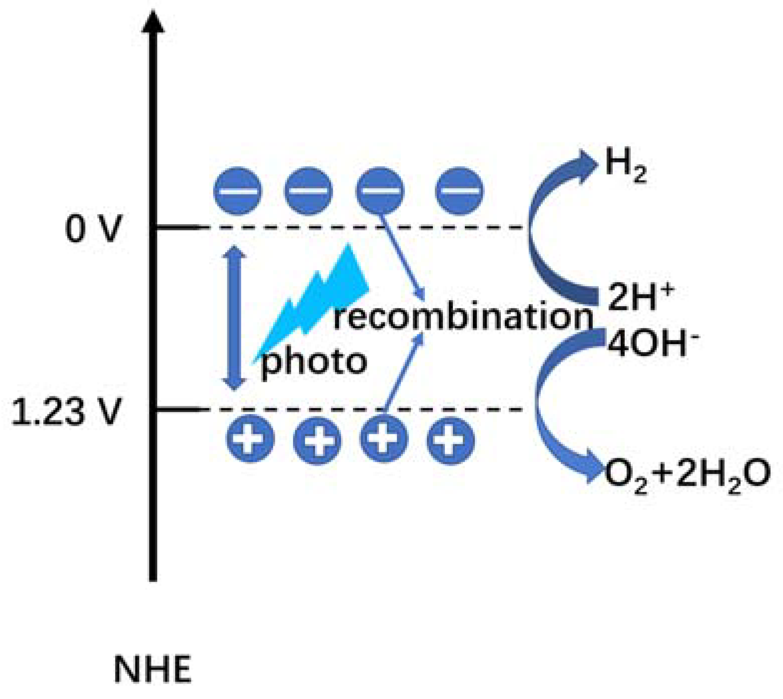
1. Introduction
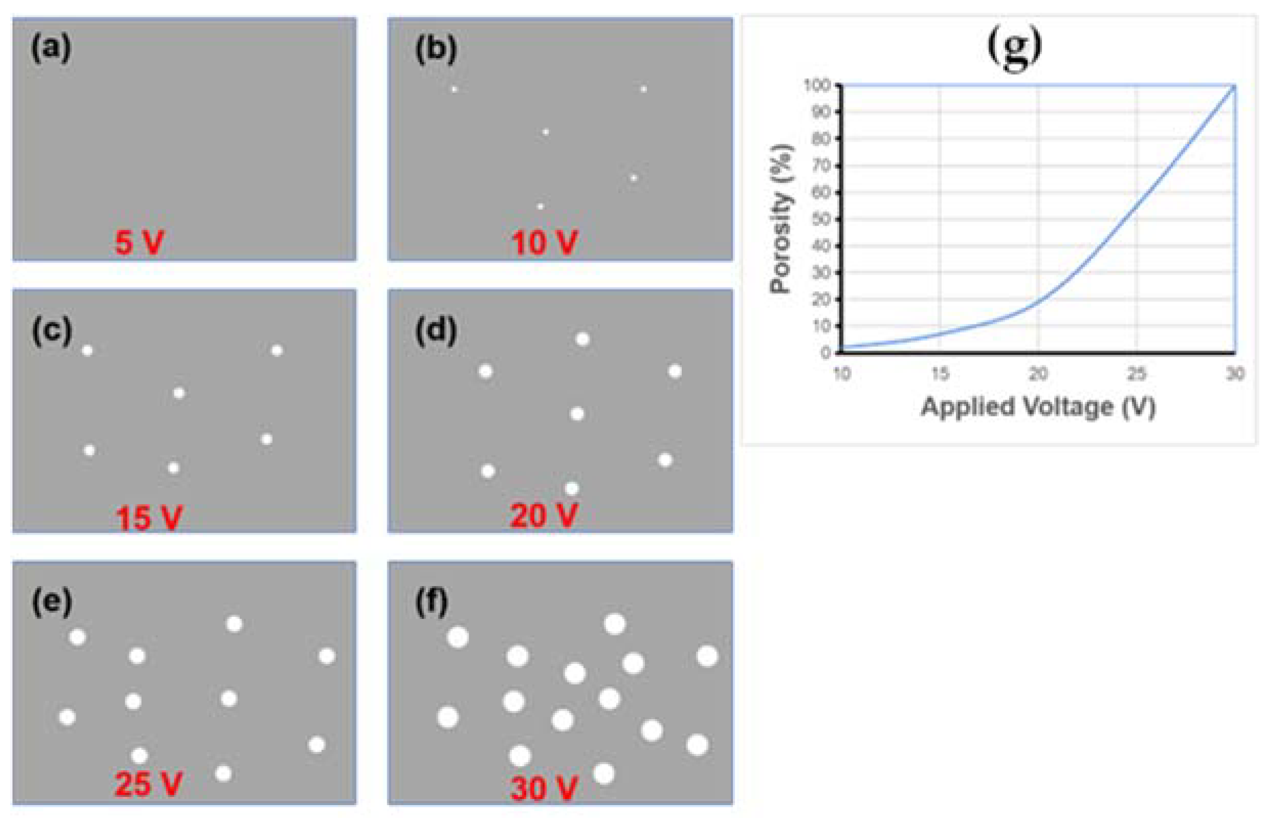
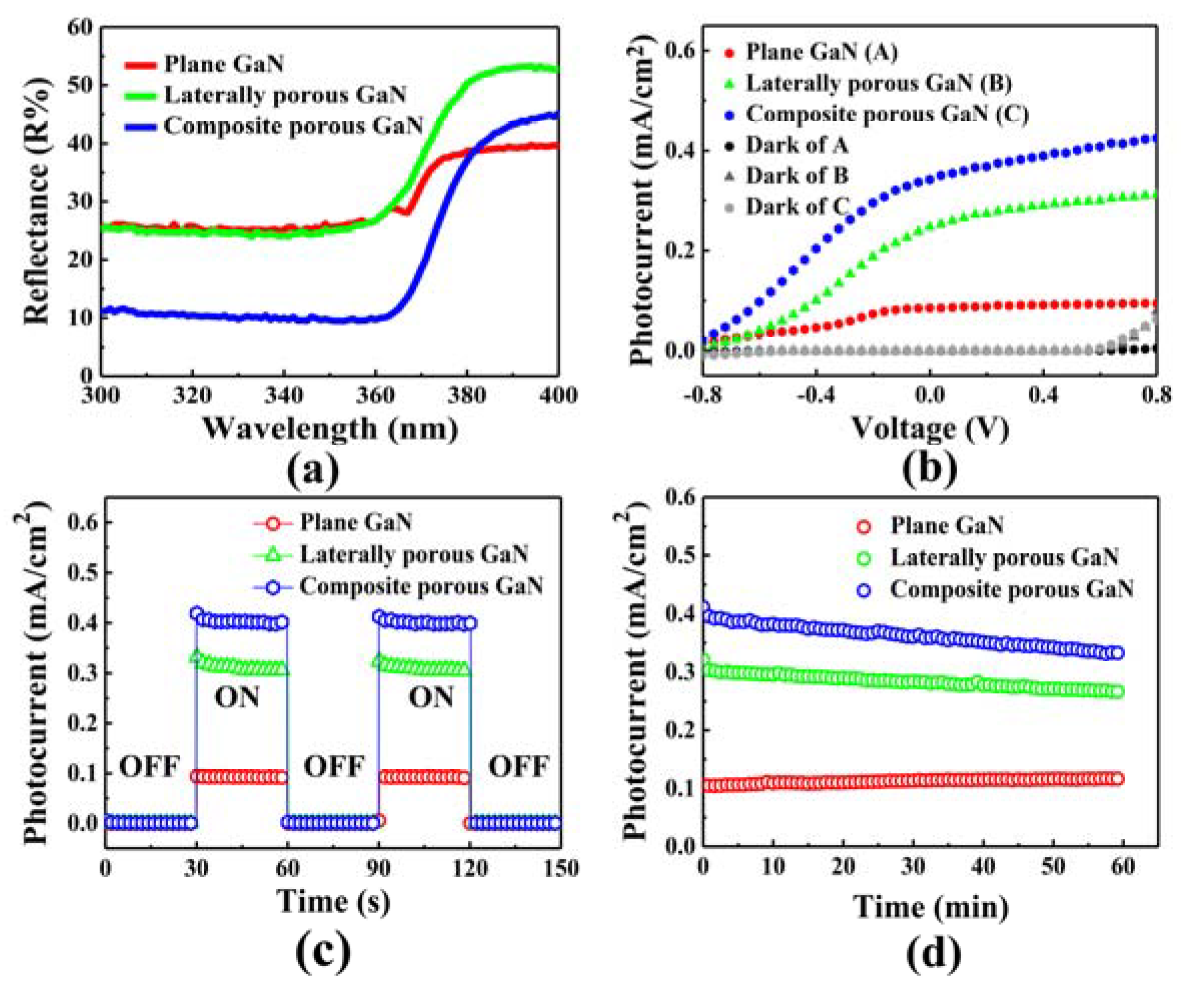
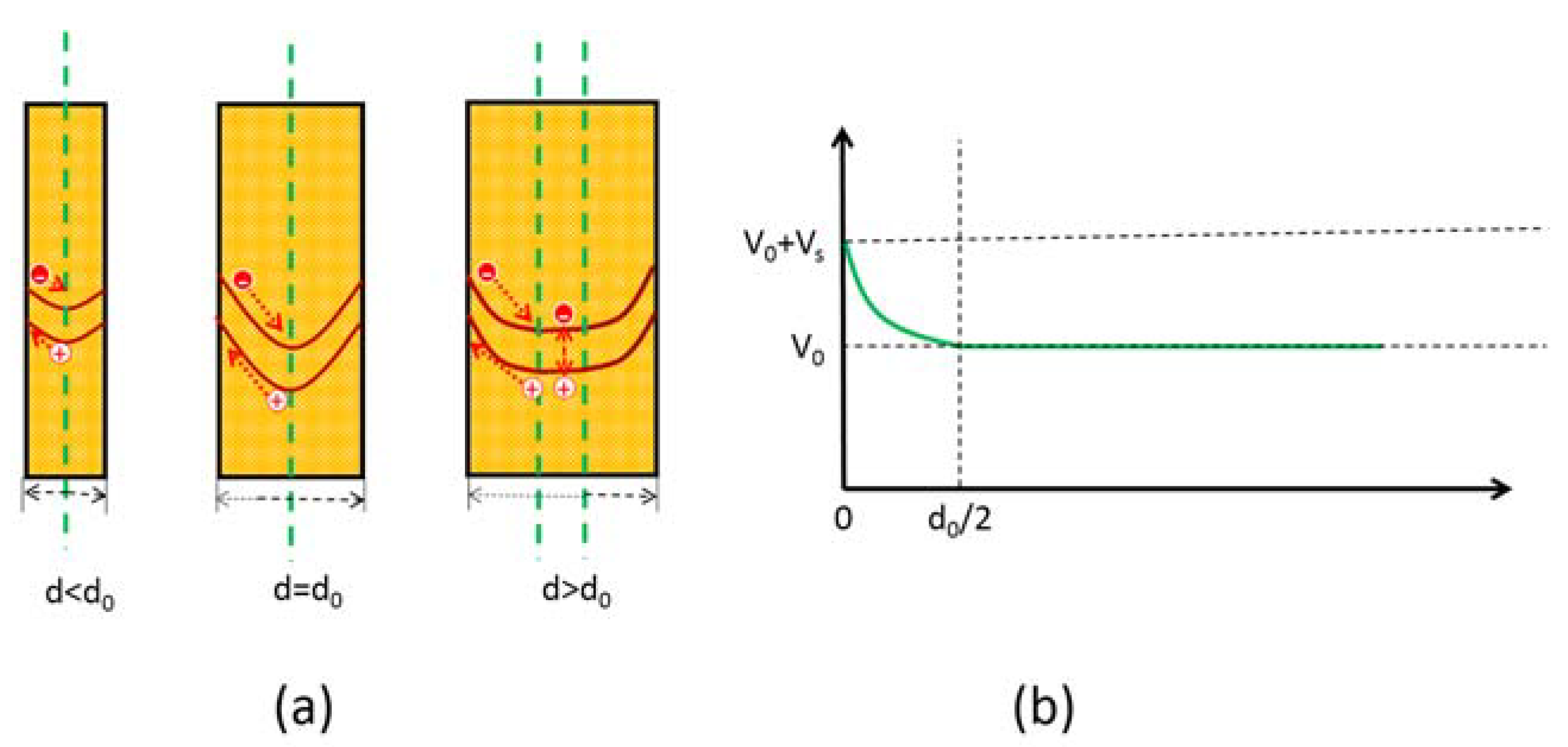
2. Lateral Nanoporous GaN
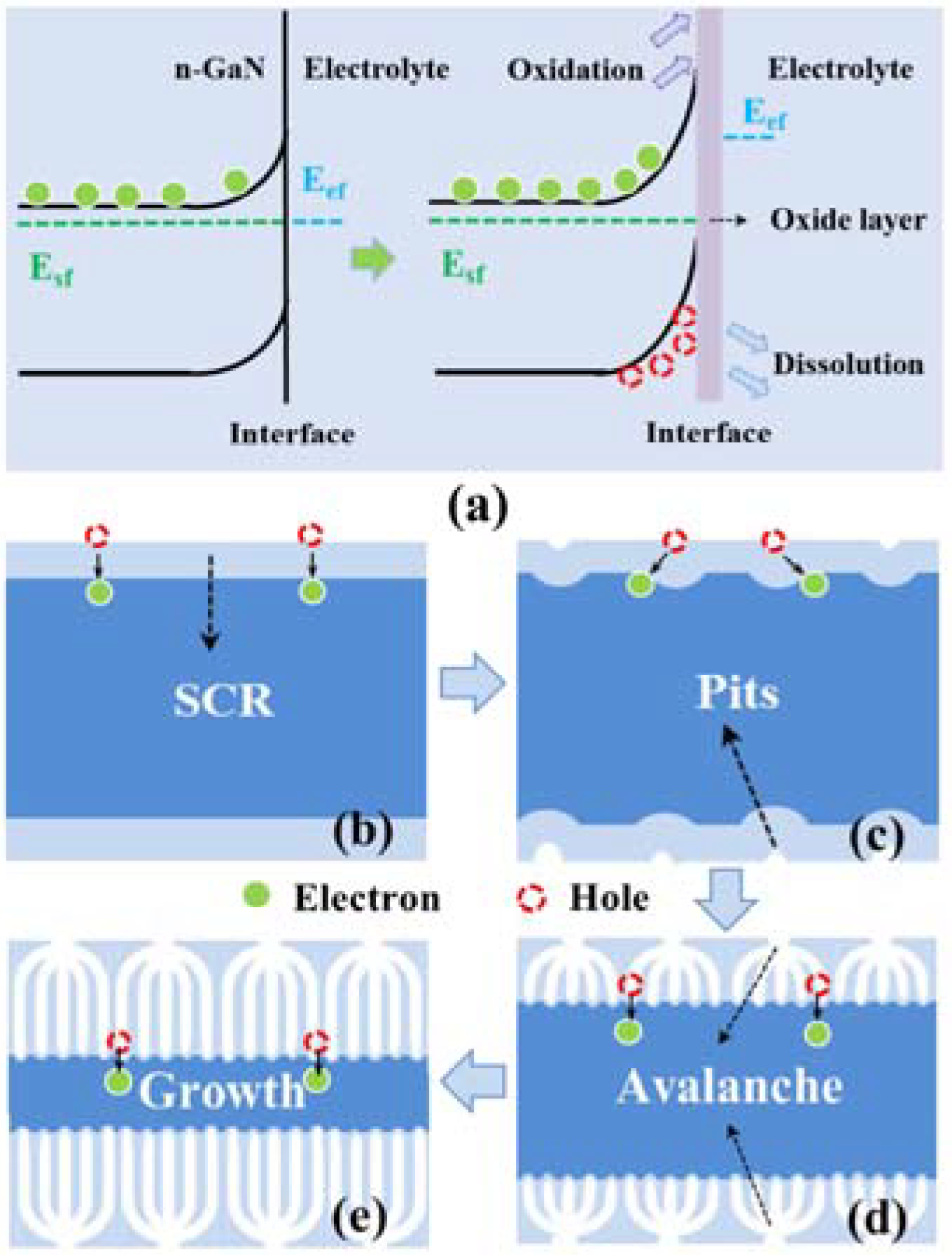
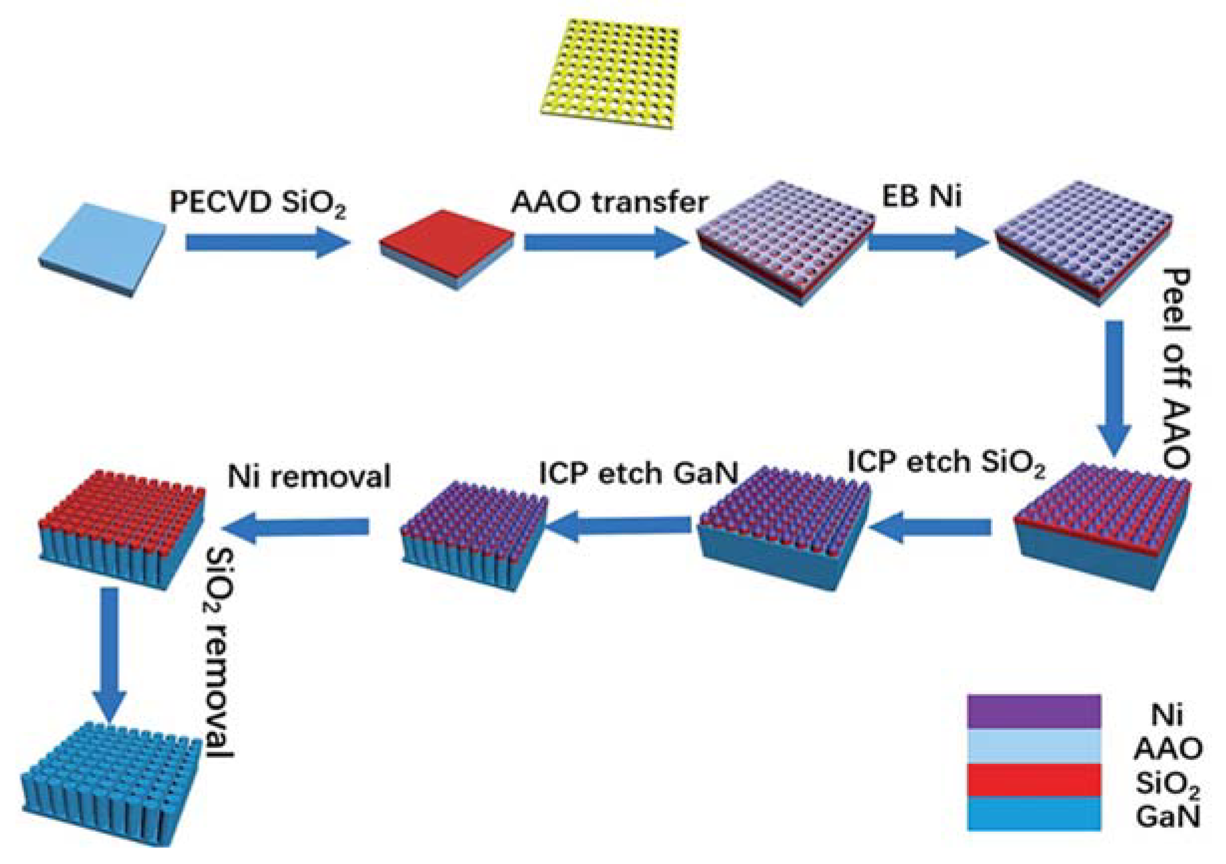
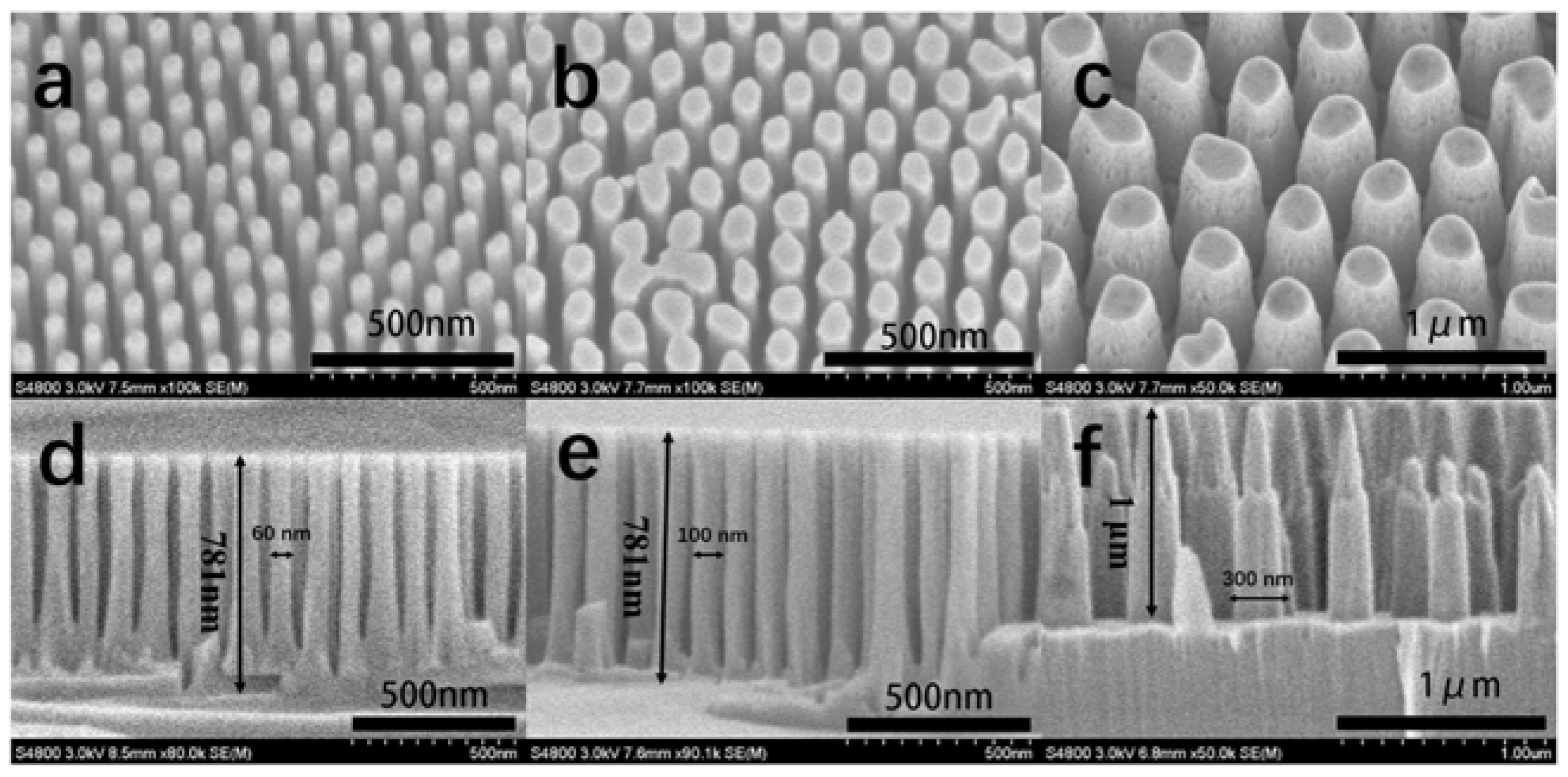
3. Vertical GaN Nanopores
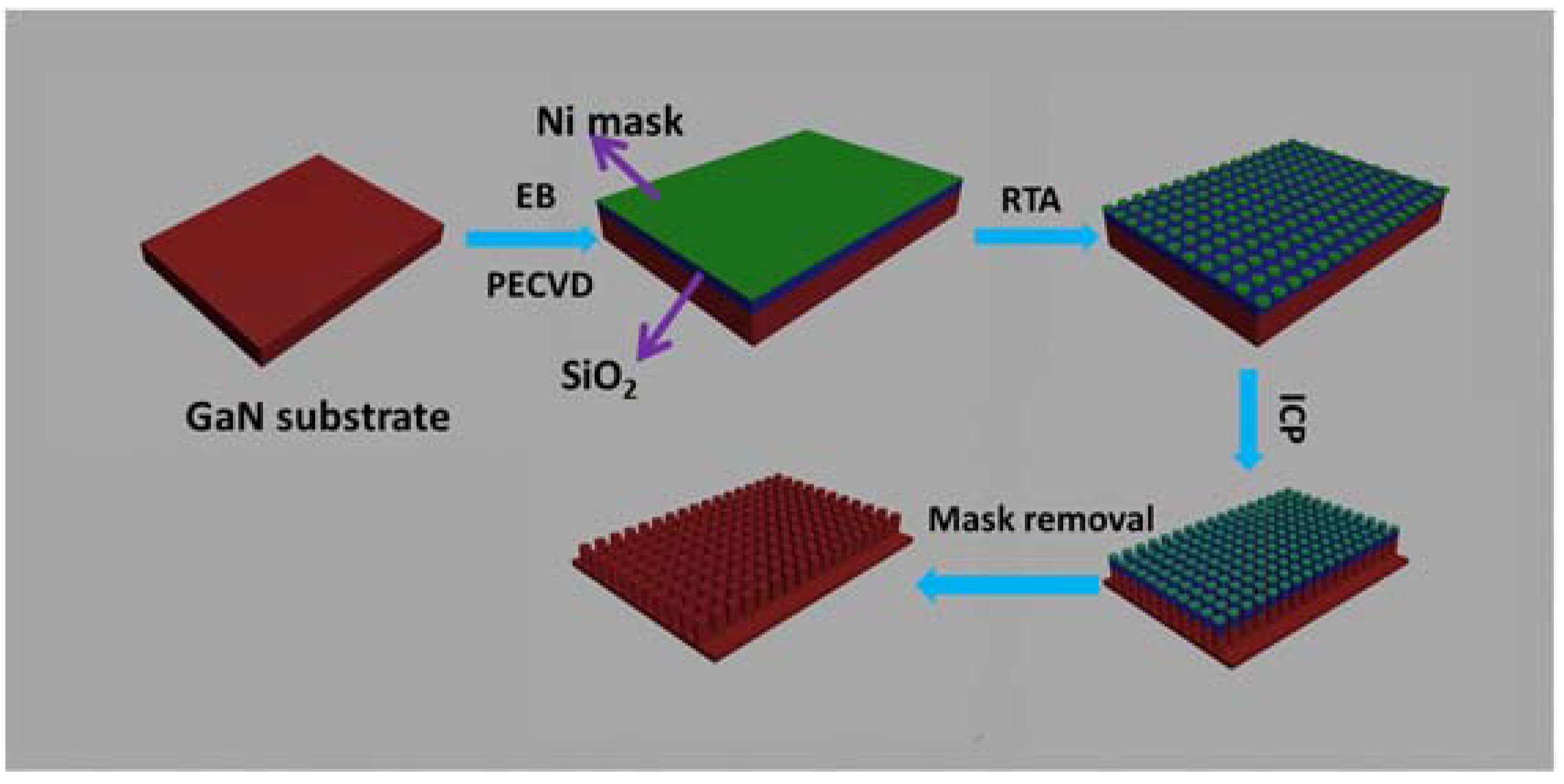
4. GaN Nanocolumns
5. Prospects for the Fabrication of GaN Nanocolumns
6. Conclusions
Author Contributions
Funding
Data Availability Statement
Conflicts of Interest
References
- Walter, M.G.; Warren, E.L.; McKone, J.R.; Boettcher, S.W.; Mi, Q.; Santori, E.A.; Lewis, N.S. Solar water splitting cells. Chem. Rev. 2010, 110, 6446–6473. [Google Scholar] [CrossRef] [PubMed]
- Chen, S.; Takata, T.; Domen, K. Particulate photocatalysts for overall water splitting. Nat. Rev. Mater. 2017, 2, 17050. [Google Scholar] [CrossRef]
- Wang, Z.; Li, C.; Domen, K. Recent developments in heterogeneous photocatalysts for solar-driven overall water splitting. Chem. Soc. Rev. 2019, 48, 2109–2125. [Google Scholar] [CrossRef] [PubMed]
- Hisatomi, T.; Kubota, J.; Domen, K. Recent advances in semiconductors for photocatalytic and photoelectrochemical water splitting. Chem. Soc. Rev. 2014, 43, 7520–7535. [Google Scholar] [CrossRef]
- Murphy, A.; Barnes, P.; Randeniya, L.; Plumb, I.; Grey, I.; Horne, M.; Glasscock, J. Efficiency of solar water splitting using semiconductor electrodes. Int. J. Hydrogen Energy 2006, 31, 1999–2017. [Google Scholar] [CrossRef]
- Ran, J.; Zhang, J.; Yu, J.; Jaroniec, M.; Qiao, S.Z. Earth-abundant cocatalysts for semiconductor-based photocatalytic water splitting. Chem. Soc. Rev. 2014, 43, 7787–7812. [Google Scholar] [CrossRef]
- Qi, J.; Zhang, W.; Cao, R. Solar-to-hydrogen energy conversion based on water splitting. Adv. Energy Mater. 2018, 8, 1701620. [Google Scholar] [CrossRef]
- Abe, J.O.; Popoola, A.; Ajenifuja, E.; Popoola, O. Hydrogen energy, economy and storage: Review and recommendation. Int. J. Hydrogen Energy 2019, 44, 15072–15086. [Google Scholar] [CrossRef]
- Lehman, P.; Chamberlin, C.; Pauletto, G.; Rocheleau, M. Operating experience with a photovoltaic-hydrogen energy system. Int. J. Hydrogen Energy 1997, 22, 465–470. [Google Scholar] [CrossRef]
- Wang, Q.; Hisatomi, T.; Jia, Q.; Tokudome, H.; Zhong, M.; Wang, C.; Pan, Z.; Takata, T.; Nakabayashi, M.; Shibata, N. Scalable water splitting on particulate photocatalyst sheets with a solar-to-hydrogen energy conversion efficiency exceeding 1%. Nat. Mater. 2016, 15, 611–615. [Google Scholar] [CrossRef]
- Ni, M.; Leung, M.K.; Leung, D.Y.; Sumathy, K. A review and recent developments in photocatalytic water-splitting using TiO2 for hydrogen production. Renew. Sustain. Energy Rev. 2007, 11, 401–425. [Google Scholar] [CrossRef]
- Miyoshi, A.; Nishioka, S.; Maeda, K. Water splitting on rutile TiO2-based photocatalysts. Chem. Eur. J. 2018, 24, 18204–18219. [Google Scholar] [CrossRef] [PubMed]
- Kang, Z.; Si, H.; Zhang, S.; Wu, J.; Sun, Y.; Liao, Q.; Zhang, Z.; Zhang, Y. Interface engineering for modulation of charge carrier behavior in ZnO photoelectrochemical water splitting. Adv. Funct. Mater. 2019, 29, 1808032. [Google Scholar] [CrossRef]
- Ma, M.; Huang, Y.; Liu, J.; Liu, K.; Wang, Z.; Zhao, C.; Qu, S.; Wang, Z. Engineering the photoelectrochemical behaviors of ZnO for efficient solar water splitting. J. Semicond. 2020, 41, 091702. [Google Scholar] [CrossRef]
- Kim, J.H.; Lee, J.S. BiVO4-based heterostructured photocatalysts for solar water splitting: A review. Energy Environ. Focus 2014, 3, 339–353. [Google Scholar] [CrossRef]
- Suarez, C.M.; Hernández, S.; Russo, N. BiVO4 as photocatalyst for solar fuels production through water splitting: A short review. Appl. Catal. A Gen. 2015, 504, 158–170. [Google Scholar] [CrossRef]
- Bagal, I.V.; Chodankar, N.R.; Hassan, M.A.; Waseem, A.; Johar, M.A.; Kim, D.-H.; Ryu, S.-W. Cu2O as an emerging photocathode for solar water splitting–A status review. Int. J. Hydrogen Energy 2019, 44, 21351–21378. [Google Scholar] [CrossRef]
- Moniz, S.J.; Shevlin, S.A.; Martin, D.J.; Guo, Z.-X.; Tang, J. Visible-light driven heterojunction photocatalysts for water splitting–A critical review. Energy Environ. Sci. 2015, 8, 731–759. [Google Scholar] [CrossRef]
- Kalanur, S.S.; Duy, L.T.; Seo, H. Recent progress in photoelectrochemical water splitting activity of WO3 photoanodes. Top. Catal. 2018, 61, 1043–1076. [Google Scholar] [CrossRef]
- Costa, M.B.; de Araújo, M.A.; de Lima Tinoco, M.V.; de Brito, J.F.; Mascaro, L.H. Current trending and beyond for solar-driven water splitting reaction on WO3 photoanodes. J. Energy Chem. 2022, 73, 88–113. [Google Scholar] [CrossRef]
- Shi, H.; Guo, H.; Wang, S.; Zhang, G.; Hu, Y.; Jiang, W.; Liu, G. Visible Light Photoanode Material for Photoelectrochemical Water Splitting: A Review of Bismuth Vanadate. Energy Fuels 2022, 36, 11404–11427. [Google Scholar] [CrossRef]
- Chen, Z.; Duan, X.; Wei, W.; Wang, S.; Ni, B.-J. Iridium-based nanomaterials for electrochemical water splitting. Nano Energy 2020, 78, 105270. [Google Scholar] [CrossRef]
- Takasugi, S.; Tomita, K.; Iwaoka, M.; Kato, H.; Kakihana, M. The hydrothermal and solvothermal synthesis of LiTaO3 photocatalyst: Suppressing the deterioration of the water splitting activity without using a cocatalyst. Int. J. Hydrogen Energy 2015, 40, 5638–5643. [Google Scholar] [CrossRef]
- Kudo, A.; Kato, H.; Tsuji, I. Strategies for the development of visible-light-driven photocatalysts for water splitting. Chem. Lett. 2004, 33, 1534–1539. [Google Scholar] [CrossRef]
- Coleman, V.A.; Jagadish, C. Basic properties and applications of ZnO. In Zinc Oxide Bulk, Thin Films and Nanostructures; Elsevier: Amsterdam, The Netherlands, 2006; pp. 1–20. [Google Scholar]
- Kuo, C.-H.; Huang, M.H. Morphologically controlled synthesis of Cu2O nanocrystals and their properties. Nano Today 2010, 5, 106–116. [Google Scholar] [CrossRef]
- Polo-Garzon, F.; Yang, S.Z.; Fung, V.; Foo, G.S.; Bickel, E.E.; Chisholm, M.F.; Jiang, D.-E.; Wu, Z. Controlling reaction selectivity through the surface termination of perovskite catalysts. Angew. Chem. 2017, 129, 9952–9956. [Google Scholar] [CrossRef]
- Joo, J.; Kim, T.; Lee, J.; Choi, S.I.; Lee, K. Morphology-controlled metal sulfides and phosphides for electrochemical water splitting. Adv. Mater. 2019, 31, 1806682. [Google Scholar] [CrossRef]
- Jia, H.; Guo, L.; Wang, W.; Chen, H. Recent progress in GaN-based light-emitting diodes. Adv. Mater. 2009, 21, 4641–4646. [Google Scholar] [CrossRef]
- Kozaki, T.; Nagahama, S.-i.; Mukai, T. Recent progress of high-power GaN-based laser diodes. Novel In-Plane Semicond. Lasers VI 2007, 6485, 16–23. [Google Scholar]
- Francis, D.; Wasserbauer, J.; Faili, F.; Babić, D.; Ejeckam, F.; Hong, W.; Specht, P.; Weber, E. GaN-HEMT epilayers on diamond substrates: Recent progress. Semant. Sch. 2007. [Google Scholar]
- Chow, T.P. Progress in high voltage SiC and GaN power switching devices. In Proceedings of the Materials Science Forum, Lombok, Indonesia, 12–13 November 2014; pp. 1077–1082. [Google Scholar]
- Paskova, T.; Evans, K.R. GaN substrates—Progress, status, and prospects. IEEE J. Sel. Top. Quantum Electron. 2009, 15, 1041–1052. [Google Scholar] [CrossRef]
- Khurgin, J.; Ding, Y.J.; Jena, D. Hot phonon effect on electron velocity saturation in GaN: A second look. Appl. Phys. Lett. 2007, 91, 252104. [Google Scholar] [CrossRef]
- Ueno, M.; Yoshida, M.; Onodera, A.; Shimomura, O.; Takemura, K. Stability of the wurtzite-type structure under high pressure: GaN and InN. Phys. Rev. B 1994, 49, 14. [Google Scholar] [CrossRef] [PubMed]
- Kuykendall, T.; Ulrich, P.; Aloni, S.; Yang, P. Complete composition tunability of InGaN nanowires using a combinatorial approach. Nat. Mater. 2007, 6, 951–956. [Google Scholar] [CrossRef]
- Kocha, S.S.; Peterson, M.W.; Arent, D.J.; Redwing, J.M.; Tischler, M.A.; Turner, J.A. Electrochemical Investigation of the Gallium Nitride-Aqueous Electrolyte Interface. J. Electrochem. Soc. 1995, 142, L238–L240. [Google Scholar] [CrossRef]
- Fujii, K.; Iwaki, Y.; Masui, H.; Baker, T.J.; Iza, M.; Sato, H.; Kaeding, J.; Yao, T.; Speck, J.S.; DenBaars, S.P. Photoelectrochemical properties of nonpolar and semipolar GaN. Jpn. J. Appl. Phys. 2007, 46, 6573. [Google Scholar] [CrossRef]
- Fujii, K.; Ohkawa, K. Photoelectrochemical properties of p-type GaN in comparison with n-type GaN. Jpn. J. Appl. Phys. 2005, 44, L909. [Google Scholar] [CrossRef]
- Fujii, K.; Karasawa, T.; Ohkawa, K. Hydrogen gas generation by splitting aqueous water using n-type GaN photoelectrode with anodic oxidation. Jpn. J. Appl. Phys. 2005, 44, L543. [Google Scholar] [CrossRef]
- Ono, M.; Fujii, K.; Ito, T.; Iwaki, Y.; Hirako, A.; Yao, T.; Ohkawa, K. Photoelectrochemical reaction and H2 generation at zero bias optimized by carrier concentration of n-type GaN. J. Chem. Phys. 2007, 126, 54708. [Google Scholar] [CrossRef]
- Wallys, J.; Hoffmann, S.; Furtmayr, F.; Teubert, J.; Eickhoff, M. Electrochemical properties of GaN nanowire electrodes—Influence of doping and control by external bias. Nanotechnology 2012, 23, 165701. [Google Scholar] [CrossRef]
- Ryu, S.-W.; Zhang, Y.; Leung, B.; Yerino, C.; Han, J. Improved photoelectrochemical water splitting efficiency of nanoporous GaN photoanode. Semicond. Sci. Technol. 2011, 27, 015014. [Google Scholar] [CrossRef]
- Ebaid, M.; Kang, J.-H.; Ryu, S.-W. Controllable Synthesis of Vapor-Liquid-Solid Grown GaN Nanowires for Photoelectrochemical Water Splitting Applications. J. Electrochem. Soc. 2015, 162, H264–H270. [Google Scholar] [CrossRef]
- Jung, H.S.; Hong, Y.J.; Li, Y.; Cho, J.; Kim, Y.-J.; Yi, G.-C. Photocatalysis using GaN nanowires. ACS Nano 2008, 2, 637–642. [Google Scholar] [CrossRef] [PubMed]
- Wang, D.; Pierre, A.; Kibria, M.G.; Cui, K.; Han, X.; Bevan, K.H.; Guo, H.; Paradis, S.; Hakima, A.-R.; Mi, Z. Wafer-level photocatalytic water splitting on GaN nanowire arrays grown by molecular beam epitaxy. Nano Lett. 2011, 11, 2353–2357. [Google Scholar] [CrossRef] [PubMed]
- Kibria, M.G.; Nguyen, H.P.; Cui, K.; Zhao, S.; Liu, D.; Guo, H.; Trudeau, M.L.; Paradis, S.; Hakima, A.-R.; Mi, Z. One-step overall water splitting under visible light using multiband InGaN/GaN nanowire heterostructures. ACS Nano 2013, 7, 7886–7893. [Google Scholar] [CrossRef] [PubMed]
- Son, H.; Park, J.H.; Uthirakumar, P.; Kuznetsov, A.Y.; Lee, I.-H. Impact of chloride surface treatment on nano-porous GaN structure for enhanced water-splitting efficiency. Appl. Surf. Sci. 2020, 532, 147465. [Google Scholar] [CrossRef]
- Tseng, W.; Van Dorp, D.; Lieten, R.; Vereecken, P.; Borghs, G. Anodic etching of n-GaN epilayer into porous GaN and its photoelectrochemical properties. J. Phys. Chem. C 2014, 118, 29492–29498. [Google Scholar] [CrossRef]
- Benton, J.; Bai, J.; Wang, T. Utilisation of GaN and InGaN/GaN with nanoporous structures for water splitting. Appl. Phys. Lett. 2014, 105, 223902. [Google Scholar] [CrossRef]
- Cao, D.; Xiao, H.; Fang, J.; Liu, J.; Gao, Q.; Liu, X.; Ma, J. Photoelectrochemical water splitting on nanoporous GaN thin films for energy conversion under visible light. Mater. Res. Express 2017, 4, 015019. [Google Scholar] [CrossRef]
- Li, Z.; Xu, Z.; Li, D.; Wu, A.; Ruan, R. A nanoporous GaN photoelectrode on patterned sapphire substrates for high-efficiency photoelectrochemical water splitting. J. Alloys Compd. 2019, 803, 748–756. [Google Scholar] [CrossRef]
- Liu, J.; Yang, X.; Chen, R.; Feng, B.; Zhu, H.; Luan, C.; Xiao, H. Vertical nanoporous GaN substrates for photonic engineering: Lu2O3: Eu single crystal thin films as an example. J. Alloys Compd. 2022, 892, 162069. [Google Scholar] [CrossRef]
- Yang, C.; Liu, L.; Zhu, S.; Yu, Z.; Xi, X.; Wu, S.; Cao, H.; Li, J.; Zhao, L. GaN with Laterally Aligned Nanopores to Enhance the Water Splitting. J. Phys. Chem. C 2017, 121, 7331–7336. [Google Scholar] [CrossRef]
- Yang, C.; Xi, X.; Yu, Z.; Cao, H.; Li, J.; Lin, S.; Ma, Z.; Zhao, L. Light modulation and water splitting enhancement using a composite porous GaN structure. ACS Appl. Mater. Interfaces 2018, 10, 5492–5497. [Google Scholar] [CrossRef] [PubMed]
- Son, H.; Uthirakumar, P.; Chung, T.-H.; Polyakov, A.; Lee, I.-H. Influence of Ga-halogen bond formation at the interface of nanoporous GaN photoelectrodes for enhanced photoelectrochemical water splitting efficiency. Appl. Surf. Sci. 2021, 547, 149105. [Google Scholar] [CrossRef]
- Sekiguchi, H.; Kishino, K.; Kikuchi, A. Ti-mask selective-area growth of GaN by RF-plasma-assisted molecular-beam epitaxy for fabricating regularly arranged InGaN/GaN nanocolumns. Appl. Phys. Express 2008, 1, 124002. [Google Scholar] [CrossRef]
- Medvedev, O.; Puzyk, M.; Usikov, A.; Helava, H.; Makarov, Y.N. Solar water splitting with III-N nanocolumn structures. In Proceedings of the Journal of Physics: Conference Series; IOP Publishing: Bristol, UK, 2017; p. 052022. [Google Scholar]
- Tyagi, P.; Ramesh, C.; Kaswan, J.; Dhua, S.; John, S.; Shukla, A.K.; Roy, S.C.; Kushvaha, S.S.; Muthusamy, S.K. Direct growth of self-aligned single-crystalline GaN nanorod array on flexible Ta foil for photocatalytic solar water-splitting. J. Alloys Compd. 2019, 805, 97–103. [Google Scholar] [CrossRef]
- Han, S.; Noh, S.; Shin, J.; Yu, Y.-T.; Lee, C.-R.; Kim, J.S. Improvement in the photoelectrochemical water-splitting performance using GaN nanowires with bundle structures. J. Mater. Chem. C 2021, 9, 12802–12810. [Google Scholar] [CrossRef]
- AlOtaibi, B.; Harati, M.; Fan, S.; Zhao, S.; Nguyen, H.; Kibria, M.; Mi, Z. High efficiency photoelectrochemical water splitting and hydrogen generation using GaN nanowire photoelectrode. Nanotechnology 2013, 24, 175401. [Google Scholar]
- AlOtaibi, B.; Fan, S.; Wang, D.; Ye, J.; Mi, Z. Wafer-level artificial photosynthesis for CO2 reduction into CH4 and CO using GaN nanowires. ACS Catal. 2015, 5, 5342–5348. [Google Scholar] [CrossRef]
- Kibria, M.; Chowdhury, F.; Zhao, S.; AlOtaibi, B.; Trudeau, M.; Guo, H.; Mi, Z. Visible light-driven efficient overall water splitting using p-type metal-nitride nanowire arrays. Nat. Commun. 2015, 6, 6797. [Google Scholar] [CrossRef]
- Wu, S.; Wang, L.; Liu, Z.; Yi, X.; Huang, Y.; Yang, C.; Wei, T.; Yan, J.; Yuan, G.; Wang, J. Ultrafast growth of horizontal GaN nanowires by HVPE through flipping the substrate. Nanoscale 2018, 10, 5888–5896. [Google Scholar] [CrossRef]
- Wu, S.; Wang, L.; Yi, X.; Liu, Z.; Yan, J.; Yuan, G.; Wei, T.; Wang, J.; Li, J. Crystallographic orientation control and optical properties of GaN nanowires. RSC Adv. 2018, 8, 2181–2187. [Google Scholar] [CrossRef] [PubMed]
- Gottschalch, V.; Wagner, G.; Bauer, J.; Paetzelt, H.; Shirnow, M. VLS growth of GaN nanowires on various substrates. J. Cryst. Growth 2008, 310, 5123–5128. [Google Scholar] [CrossRef]
- Damilano, B.; Coulon, P.-M.; Vézian, S.; Brändli, V.; Duboz, J.-Y.; Massies, J.; Shields, P.A. Top-down fabrication of GaN nano-laser arrays by displacement Talbot lithography and selective area sublimation. Appl. Phys. Express 2019, 12, 045007. [Google Scholar] [CrossRef]
- Roshko, A.; Brubaker, M.; Blanchard, P.; Harvey, T.; Bertness, K.A. Selective area growth and structural characterization of GaN nanostructures on Si (111) substrates. Crystals 2018, 8, 366. [Google Scholar] [CrossRef]
- Bai, J.; Wang, Q.; Wang, T. Greatly enhanced performance of InGaN/GaN nanorod light emitting diodes. Phys. Status Solid 2012, 209, 477–480. [Google Scholar] [CrossRef]
- Behzadirad, M.; Nami, M.; Wostbrock, N.; Zamani Kouhpanji, M.R.; Feezell, D.F.; Brueck, S.R.; Busani, T. Scalable top-down approach tailored by interferometric lithography to achieve large-area single-mode GaN nanowire laser arrays on sapphire substrate. ACS Nano 2018, 12, 2373–2380. [Google Scholar] [CrossRef]
- Damilano, B.; Vézian, S.; Brault, J.; Alloing, B.; Massies, J. Selective area sublimation: A simple top-down route for GaN-based nanowire fabrication. Nano Lett. 2016, 16, 1863–1868. [Google Scholar] [CrossRef]
- Han, N.; Liu, P.; Jiang, J.; Ai, L.; Shao, Z.; Liu, S. Recent advances in nanostructured metal nitrides for water splitting. J. Mater. Chem. A 2018, 6, 19912–19933. [Google Scholar] [CrossRef]
- Fernández-Garrido, S.; Auzelle, T.; Lähnemann, J.; Wimmer, K.; Tahraoui, A.; Brandt, O. Top-down fabrication of ordered arrays of GaN nanowires by selective area sublimation. Nanosc. Adv. 2019, 1, 1893–1900. [Google Scholar] [CrossRef]
- Xi, X.; Yang, C.; Cao, H.; Yu, Z.; Li, J.; Lin, S.; Ma, Z.; Zhao, L. GaN nanocolumns fabricated by self-assembly Ni mask and its enhanced photocatalytic performance in water splitting. Appl. Surf. Sci. 2018, 462, 310–315. [Google Scholar] [CrossRef]
- Wang, J.; Xi, X.; Lin, S.; Li, X.; Hu, T.; Zhao, L. Effective photocatalytic water splitting enhancement using GaN/ZnO/NiO core/shell nanocolumns. J. Renew. Sustain. Energy 2021, 13, 013702. [Google Scholar] [CrossRef]
- Narangari, P.R.; Karuturi, S.K.; Lysevych, M.; Tan, H.H.; Jagadish, C. Improved photoelectrochemical performance of GaN nanopillar photoanodes. Nanotechnology 2017, 28, 154001. [Google Scholar] [CrossRef] [PubMed]
- Kim, Y.J.; Lee, G.J.; Kim, S.; Min, J.-W.; Jeong, S.Y.; Yoo, Y.J.; Lee, S.; Song, Y.M. Efficient light absorption by GaN truncated nanocones for high performance water splitting applications. ACS Appl. Mater. Interfaces 2018, 10, 28672–28678. [Google Scholar] [CrossRef]
- Li, J.; Xi, X.; Li, X.; Lin, S.; Ma, Z.; Xiu, H.; Zhao, L. Ultra-High and Fast Ultraviolet Response Photodetectors Based on Lateral Porous GaN/Ag Nanowires Composite Nanostructure. Adv. Opt. Mater. 2020, 8, 1902162. [Google Scholar] [CrossRef]
- Li, X.; Yang, C.; Li, J.; Xi, X.; Ma, Z.; Lin, S.; Zhao, L. Controllable fabrication of lateral periodic nanoporous GaN and its enhanced photocatalytic water splitting performance. Appl. Surf. Sci. 2020, 526, 146618. [Google Scholar] [CrossRef]
- Li, X.; Hu, T.; Lin, S.; Ma, Z.; Wang, J.; Zhao, L. Fabrication of layer-ordered porous GaN for photocatalytic water splitting. Int. J. Hydrogen Energy 2021, 46, 7878–7884. [Google Scholar] [CrossRef]
- Hu, T.; Liu, C.; Liu, J. High-Efficient Water Splitting Using Nanostructured Conical GaN. J. Electrochem. Soc. 2022, 169, 066514. [Google Scholar] [CrossRef]
- AlOtaibi, B.; Nguyen, H.; Zhao, S.; Kibria, M.; Fan, S.; Mi, Z. Highly stable photoelectrochemical water splitting and hydrogen generation using a double-band InGaN/GaN core/shell nanowire photoanode. Nano Lett. 2013, 13, 4356–4361. [Google Scholar] [CrossRef]
- Kibria, M.G.; Qiao, R.; Yang, W.; Boukahil, I.; Kong, X.; Chowdhury, F.A.; Trudeau, M.L.; Ji, W.; Guo, H.; Himpsel, F. Atomic-Scale Origin of Long-Term Stability and High Performance of p-GaN Nanowire Arrays for Photocatalytic Overall Pure Water Splitting. Adv. Mater. 2016, 28, 8388–8397. [Google Scholar] [CrossRef]
- Xi, X.; Li, J.; Ma, Z.; Li, X.; Zhao, L. Enhanced water splitting performance of GaN nanowires fabricated using anode aluminum oxide templates. RSC Adv. 2019, 9, 14937–14943. [Google Scholar] [CrossRef] [PubMed]


Disclaimer/Publisher’s Note: The statements, opinions and data contained in all publications are solely those of the individual author(s) and contributor(s) and not of MDPI and/or the editor(s). MDPI and/or the editor(s) disclaim responsibility for any injury to people or property resulting from any ideas, methods, instructions or products referred to in the content. |
© 2023 by the authors. Licensee MDPI, Basel, Switzerland. This article is an open access article distributed under the terms and conditions of the Creative Commons Attribution (CC BY) license (https://creativecommons.org/licenses/by/4.0/).
Share and Cite
Xi, X.; Zhao, L.; Li, T.; Li, X.; Yang, C. The Fabrication of GaN Nanostructures Using Cost-Effective Methods for Application in Water Splitting. Crystals 2023, 13, 873. https://doi.org/10.3390/cryst13060873
Xi X, Zhao L, Li T, Li X, Yang C. The Fabrication of GaN Nanostructures Using Cost-Effective Methods for Application in Water Splitting. Crystals. 2023; 13(6):873. https://doi.org/10.3390/cryst13060873
Chicago/Turabian StyleXi, Xin, Lixia Zhao, Tuo Li, Xiaodong Li, and Chao Yang. 2023. "The Fabrication of GaN Nanostructures Using Cost-Effective Methods for Application in Water Splitting" Crystals 13, no. 6: 873. https://doi.org/10.3390/cryst13060873
APA StyleXi, X., Zhao, L., Li, T., Li, X., & Yang, C. (2023). The Fabrication of GaN Nanostructures Using Cost-Effective Methods for Application in Water Splitting. Crystals, 13(6), 873. https://doi.org/10.3390/cryst13060873