Article

Composition Dependence Structural and Optical Properties of Silicon Germanium (SiχGe1−χ) Thin Films

by
Syafiqa Nasir
1,
Fuei Pien Chee
2,*,
Bablu Kumar Ghosh
1,*,
Muhammad Izzuddin Rumaling
2,
Rosfayanti Rasmidi
3,
Mivolil Duinong
2 and
Floressy Juhim
2
1
Faculty of Engineering, Universiti Malaysia Sabah, Kota Kinabalu 88400, Sabah, Malaysia
2
Faculty of Science and Natural Resources, Kota Kinabalu 88400, Sabah, Malaysia
3
Faculty of Applied Science, Universiti Teknologi MARA Sabah Branch, Kota Kinabalu 88400, Sabah, Malaysia
*
Authors to whom correspondence should be addressed.
Crystals 2023, 13(5), 791; https://doi.org/10.3390/cryst13050791
Submission received: 9 April 2023 / Revised: 5 May 2023 / Accepted: 5 May 2023 / Published: 9 May 2023
(This article belongs to the Special Issue Silicon-Based Photovoltaic Materials and Devices)

Abstract

:

Highlights

  • The research is focused on analyzing the structural properties of SiGe alloys with different compositions, with a particular focus on the effect of annealing temperature on the quality of the crystalline structure.
  • The findings suggest that the quality of the crystalline structure in SiGe alloys improves as annealing temperature increases, and that this is particularly noticeable in alloys with higher percentages of Ge. This indicates that the thermal treatment of SiGe alloys is an important factor in optimizing their properties for various applications.
  • Understanding the structural properties of SiGe alloys is important for a wide range of technological applications, including electronics, optoelectronics, and thermoelectric devices.

Abstract

This study investigates the structural and optical characteristics of Silicon Germanium (SiGe) thin films with varying compositions and annealing temperatures for potential use in electronic and optoelectronic devices. Si0.8Ge0.2 and Si0.9Ge0.1 films were deposited onto a high-temperature quartz substrate and annealed at 600 °C, 700 °C, and 800 °C before being evaluated using an X-Ray Diffractometer (XRD), Atomic Force Microscopy (AFM), and a UV-Vis Spectrometer for structural and optical properties. The results show that increasing the annealing temperature results in an increase in crystalline size for both compositions. The transmittance for Si0.8Ge0.2 decreases slightly with increasing temperature, while Si0.9Ge0.1 remains constant. The optical band gap for Si0.9Ge0.1 thin film is 5.43 eV at 800 °C, while Si0.8Ge0.2 thin film is 5.6 eV at the same annealing temperature. XRD data and surface analysis reveal significant differences between the band edges of SiGe nano-structure materials and bulk crystals. However, the possibility of a SiGe nano-crystal large band gap requires further investigation based on our study and related research works.

1. Introduction

The widespread consumption of coal and petroleum has a devastating impact on global warming and climate change. In order to mitigate these environmental issues, it is essential to generate eco-friendly energy [1,2]. SiGe semiconductor is a transparent material that offers numerous technical and technological advantages for the future. It has a wide range of applications, including uses for solar cells, transistors, photodetectors, and thermoelectric devices. Optical transparency is also required as it allows for light emission through the wavelength. However, the production of SiGe semiconductor requires a unique production procedure, requiring that it be put on a high-temperature substrate [3,4]. The minimization of optoelectrical losses in solar photovoltaic cells that use several contact approaches is introduced. However, a low resistance transparent barrier with superior electrical performance has yet to be achieved. Therefore, there is significant potential for the development of a low optoelectrical p-contact.
Silicon-doped germanium offers its own stability and efficient spectral utility; this allows for modulation in the optical window through bandgap engineering [5]. Achieving these specialties might be possible by changing the Ge mole fraction in the SiGe material [5]. According to Fathipour et al., the addition of Ge mole fraction in the c-Si thin film could reduce the bandgap and increase the absorption coefficient of the thin film. On the other hand, the addition of SiGe mole fraction in the composition might affect the structural and optical characterization of the thin film [6]. Increasing the Ge content in a composition may be beneficial due to its stability and improved performance [7]. Additionally, SiGe alloy MOSFET stressors are utilized to induce strain into the Si and Ge channels [8]. The production of nanocomposites is a viable method for lowering SiGe alloys’ lattice thermal conductivity [9].
It has been reported that lower deposition temperatures are more effective in improving carrier lifetimes when compared to higher temperatures due to less substantial degradation of Si characteristics [10]. CdTe solar cells have been found to exhibit reduced efficiency with increasing temperature, while mcSi and Si modules have been shown to have higher efficiency when compared to CdTe solar cells [4,5,6,7,8,9,10,11]. Moreover, SiGe thin film is well-known for its higher transparency and exhibits superior photo-electrical properties for future transparent solar cells. In addition, these similar complex material systems have been successfully addressed by ab initio calculations, including the structural and growth aspects [12].
The deposition of SiGe thin film is achieved using the Radio Frequency sputtering method. This method is considered to be the most effective method for depositing a wide range of thin film materials under vacuum conditions [13]. Previous research has found that Si0.5Ge0.5 grown by chemical vapor deposition exhibits an optical bandgap of approximately 1 eV, with high defect concentration at lower growth temperatures [14]. Si solar cell is realized to have the best module efficiency, with both chemically and electrically appealing designs for the aSi:H buffer and emitter, as well as metal oxide back passivation [15]. In this research, the structural and optical characterization for both Si0.8Ge0.2 and Si0.9Ge0.1 were analyzed.

2. Experimental Details

To prepare the quartz glass substrate for the sputtering process, it was first cleaned in an ultrasonic bath for 15 min using a combination of distilled water, ethanol, and acetone. The quartz substrate was then rinsed with distilled water and blown dry with an inert gas (nitrogen gas). Si0.8Ge0.2 and Si0.9Ge0.1 layers were sputtered on the cleaned quartz substrate using a Radio Frequency sputtering machine for about 30 min. Prior to sputtering, the quartz substrate was heated to 900 °C in a furnace. The sputtering process was carried out under the following conditions: a sputtering power of 98 W, a working pressure of 3 mTorr, and a temperature of 900°. A SiGe target was positioned parallel to the substrate to ensure even distribution. The process involved introducing argon gas at a low pressure of less than 0.4 mTorr, causing the gas atoms to become ionized and form plasma with the aid of electrons and neutral atoms. The plasma was then deposited onto the quartz substrate, resulting in the formation of a thin film. Table 1 shows the thin film composition and target parameters used in the deposition process.
The sputtering time was kept constant throughout the process to ensure a constant growth thickness of 300 nm for both SiGe compositions. Following the sputtering process, all the samples were annealed inside a furnace for 30 min at varying temperatures of 600 °C, 700 °C, and 800 °C for both SiGe compositions. A Bruker Multimode 8-HR, an atomic force microscope, was used to analyze and study the surface and morphological properties of the deposited SiGe thin film. Additionally, the optical properties of the samples were observed using a Lambda EZ210 UV-Vis spectrometer to measure the optical transmittance and calculate the optical bandgap of the samples.

3. Result and Discussion

3.1. Structural Properties of Si0.8Ge0.2 and Si0.9Ge0.1 Thin Film

XRD data has been analyzed and there are two peaks observed at 64.4° (4 0 0) and 77.5° (3 3 1) for both Si0.8Ge0.2 and Si0.9Ge0.1 as in Figure 1 [16,17]. From the XRD result in Figure 1, it can be seen that there is some shifting happening at 64.4°; this might be due to lattice mismatch and the sample stage.
The interplanar distance of the film samples or the lattice parameter was calculated using Equation (1).
d h k l = h 2 a 2 + k 2 b 2 + l 2 c 2
where h, k, and l are the Miller indices. From the XRD data, the increase in annealing temperature causes lattice distortion. It enhances crystal defect, as proven by the micro-strain result in Table 2 for Si0.8Ge0.2 composition for 700 °C and 800 °C annealing temperature [18]. The crystallite size for both compositions in Si0.8Ge0.2 and Si0.9Ge0.1 are calculated using the Scherrer Equation, as stated in Equation (2).
D = k λ β cos ϑ
where D is crystalline size, k is the Scherrer constant, λ is the wavelength of x-ray source, β is the FWHM in radian, and θ is the peak position in XRD analysis. The crystallite size is observed to be in nanoscale; this follows the XRD peak in Figure 1 [19]. The micro-strain of the crystallite has been calculated using the micro-strain equation as stated in Equation (3).
ε = β 4 tan θ
where ε is the micro-strain in radian, β is the line broadening at FWHM in radian, and θ is the Bragg’s angle in degree, which is half of the 2θ value in the XRD data.
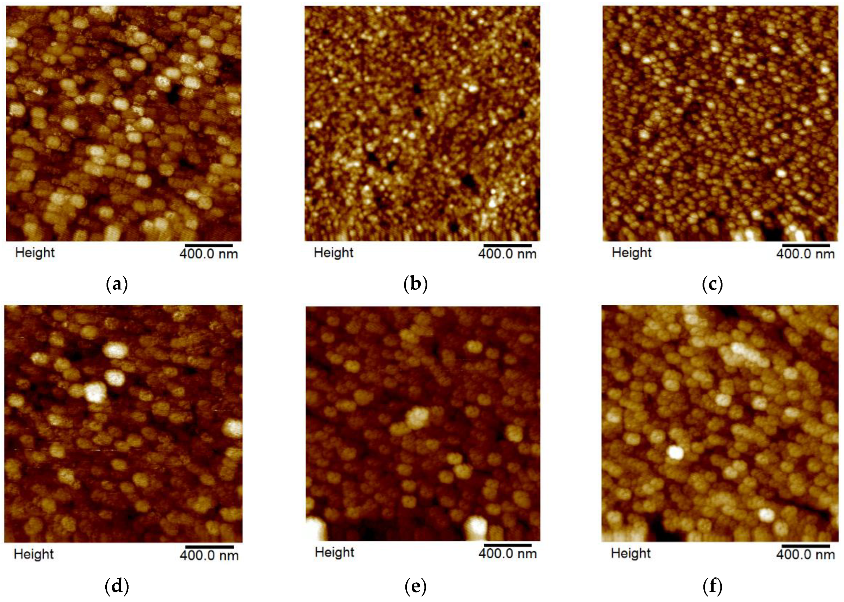
Table 2 reveals a discrepancy between the crystallite size from the XRD data and the grain size from the AFM data. Specifically, the crystallite size increases from 35.79 nm and 36.78 nm at 600 °C and 800 °C for Si0.8Ge0.2 composition, respectively, while the grain size obtained from the AFM data increases from 61.08 nm to 74.87 nm over the same temperature range. This can be explained by the fact that the crystallite size is composed of several particles that are coherent diffraction domains in X-ray diffraction and is dependent on the size of the defect-free volume, while grains are volumes inside crystalline materials with a specific orientation and are visualized without taking the degree of structural imperfection into account. The XRD data indicate that an increase in annealing temperature leads to lattice distortion and enhanced crystal defect, as evidenced by micro-strain results in Table 2 for Si0.8Ge0.2 composition at 700 °C and 800 °C annealing temperatures [18]. However, strain characteristics are also impacted by changes in composition and lead to an increase in carrier mobility [20]. Surface roughness, particle analysis, and particle density for both Si0.8Ge0.2 and Si0.9Ge0.1 were also analyzed using Atomic Force Microscopy (AFM). Figure 1 displays the crystalline image of Si0.8Ge0.2 and Si0.9Ge0.1 at different temperatures. For the Si0.8Ge0.2 composition, the lower annealing temperature resulted in a larger grain size than the higher annealing temperature. The AFM analysis in Figure 1 shows that richer grains can be observed at 700 °C and 800 °C when compared to the lower temperature. However, Si0.9Ge0.1 composition shows a constant trend in grain size from the AFM analysis, as shown in Figure 2d–f. Both compositions have larger grain sizes at an annealing temperature of 800 °C.
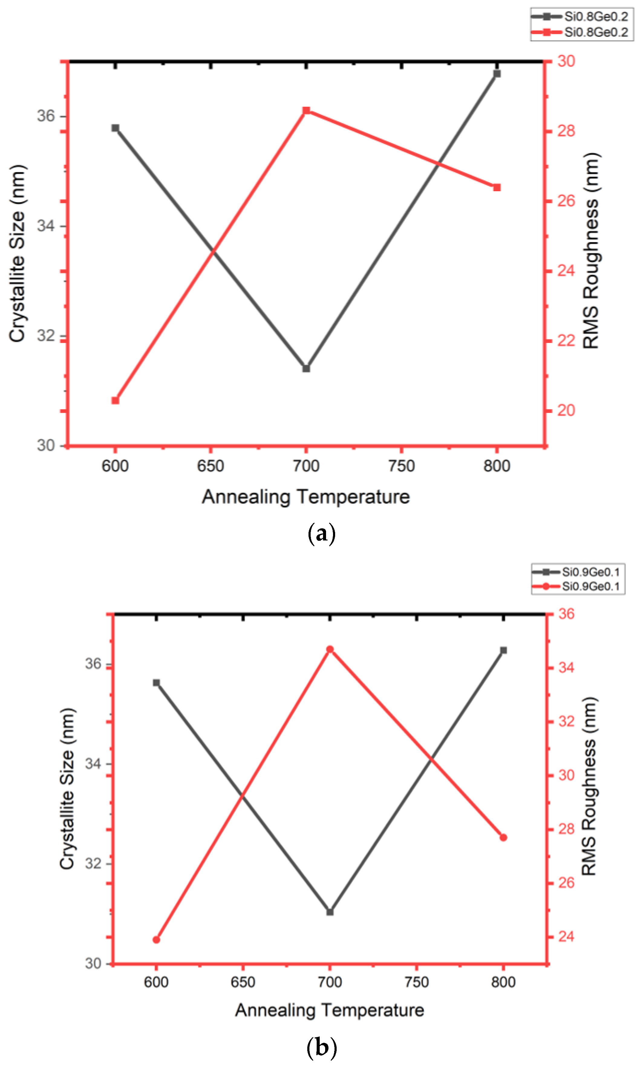
The AFM analysis was supported by the XRD data (shown in Figure 3); these data reveal the crystallite size for both SiGe compositions. Based on Figure 3, the highest roughness was observed at 700 °C for each composition, reaching 34.7 nm, and then decreased to 27.7 nm as the temperature increased. The trend was consistent for both compositions. This tendency justifies the dislocation rearrangement and removal of point defect during recovery, which could considerably lower the amount of stored energy [21,22] and weakens the bonds of the material [23,24]. Samples annealed at high temperatures have more energy trapped inside the matrix due to insufficient time for recovery between grains [21]. This may also be caused by insufficient recovery and faster grain growth rates due to higher stored energy within the samples. Table 3 shows the summary of structural properties, including particle density, for both Si0.8Ge0.2 and Si0.9Ge0.1 compositions.
Based on Table 3, the particle density for Si0.8Ge0.2 increases with the annealing temperature, whereas for Si0.9Ge0.1, the particle density decreases with increasing temperature. Particle density was determined using an Atomic Force Microscopy (AFM) nano-scope analyzer from Bruker [25]. Among the compositions, Si0.8Ge0.2 has the highest particle density, with a value of 52.486 µm−2 at 800 °C, which is higher than that of Si0.9Ge0.1. This observation suggests that Si0.8Ge0.2 has a more stable structure than Si0.9Ge0.1, consistent with the reported decrease in lattice parameter as Ge concentration increases [26]. These results support the benefits of higher particle density, such as in the double stack structure, which may increase cation disordering due to high thermal energy in the nanocrystalline system [27]. For both compositions, the highest particle roughness was observed at 700 °C, with values of 28.6 nm and 34.7 nm for Si0.8Ge0.2 and Si0.9Ge0.1, respectively.

3.2. Optical Properties Analysis for Both Si0.8Ge0.2 and Si0.9Ge0.1 at Different Annealing Temperature

The transmittance and absorbance graph from our UV-Vis analysis has been plotted for both materials at different annealing temperatures, as shown in Figure 4. At 600 °C, the transmittance of Si0.8Ge0.2 at 850 nm wavelength is 87.87%, while the transmittance for Si0.9Ge0.1 remains constant at 87.90% across all annealing temperatures. The observed trend can be attributed to the roughness of grain boundaries in Si0.9Ge0.1, which might be caused by the rapid annealing process employed for this composition [28,29].
The absorbance values obtained can be utilized to estimate the band gap energy values of the formed SiGe films. According to the absorbance data, the optical bandgap for both compositions was calculated using Equation (4) [30].
α h v h v E g 1 / 2
where α is the absorption coefficient, h v is the incident photon energy, and Eg refer to the optical bandgap [31]. Table 4 shows the summary of optical bandgap and transmittance for both compositions of SiGe.
The optical bandgap was found to be approximately 5.505 eV for Si0.8Ge0.2 at 600 °C, while the bandgap for Si0.9Ge0.1 is slightly higher (5.528 eV) at the same temperature. At 800 °C, Si0.8Ge0.2 composition has a higher bandgap (5.595 eV), while Si0.9Ge0.1 has the lowest bandgap (5.429 eV). From the optical bandgap summary in Table 4, an annealing temperature of 800 °C was found to be the most effective for Si0.9Ge0.1, resulting in a lower bandgap and, therefore, a lower recombination rate [32]. As for Si0.8Ge0.2 thin film, the structural modifications for increased quantum confinement can be attributed to the effects where the optical bandgap increases as the annealing temperature rises [33,34,35]. Overall, it was observed that the optical bandgap increases as the grain size of the nanocrystalline state increases, as seen in XRD data in Figure 1 and Table 3 [36]. It is realized that for nanocrystalline SiGe thin film, the discrepancy from the bandgap approximation might be explained by the bands’ nonparabolicity as a result of band-folding and state mixing, while holes and electrons cannot be transferred to tiny clusters [37,38]. Furthermore, explorations between the bandgap of bulk and nanocrystalline SiGe thin film have reported that the dependence on Ge concentration is consistent with the results presented in Table 3 [36]. The invariance of the shape can be described by Equation (5) [36].
E g d , x = E 0 N C + 4.58 / d 1.25
Figure 4 shows the transmittance data for both SiGe compositions. The absorption coefficient and bandgap for Si0.8Ge0.2 show a decreasing trend at 700 °C, followed by a rapid increase at 800 °C. This indicates that Si0.8Ge0.2 has a greater ability to control how far light of a specific wavelength can pass into a substance before being absorbed. On the other hand, Si0.9Ge0.1 exhibits a decreasing trend in bandgap across the temperature range, but its absorption coefficient increases. Figure 5 plots the (ahv)2 versus energy graph for both compositions to further investigate the relationship between absorption coefficient and energy. From Peng et al., the absorption edge for pure quartz glass shows a lower absorption edge than in this study. The absorption peak observed in Figure 6 indicates that the SiGe thin films are deposited on top of the quartz glass [39]. Overall, these results suggest that the optical properties of SiGe thin films are highly dependent on the composition and annealing conditions, which could have important implications for their potential applications in optoelectronics and other fields.
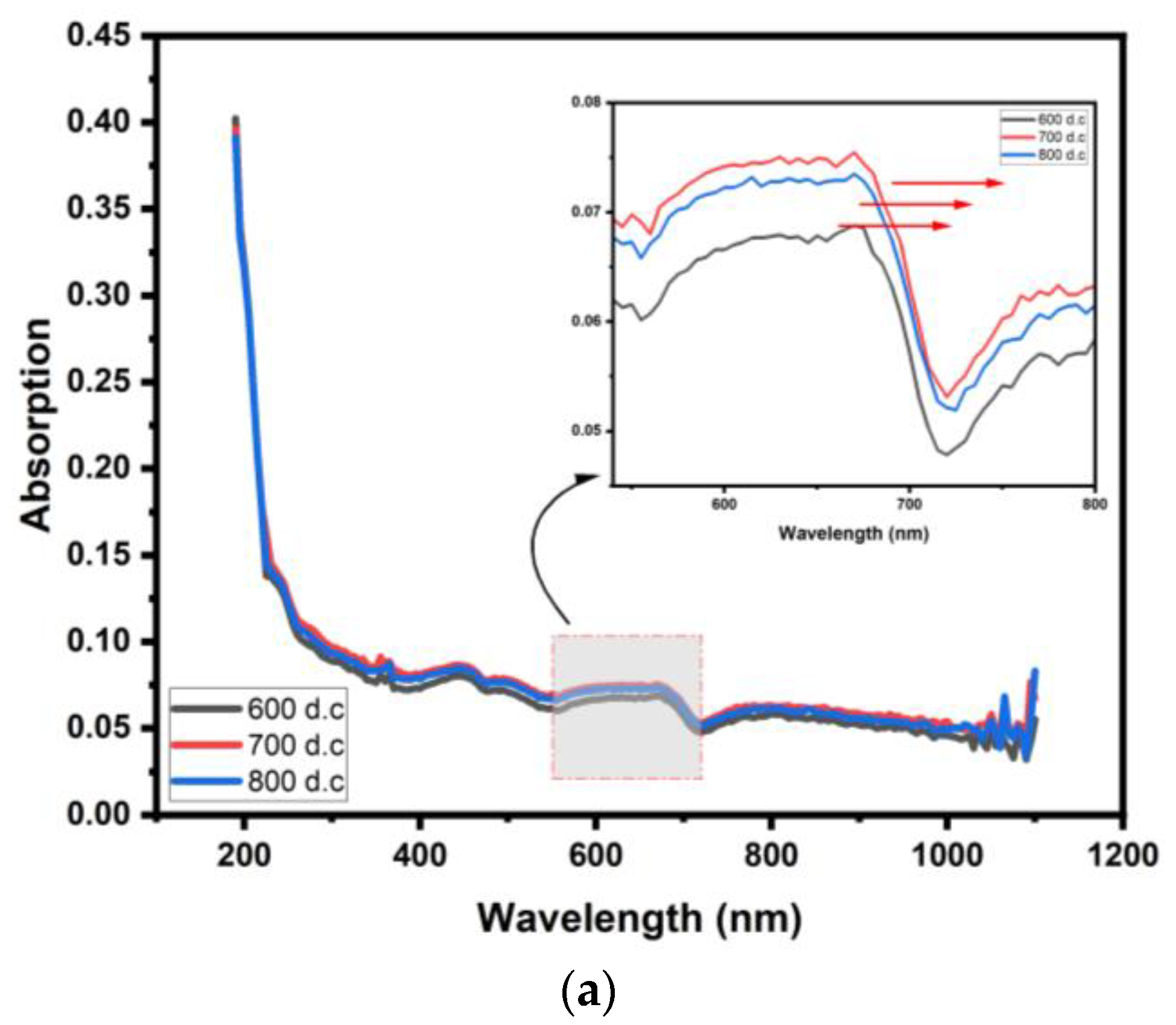
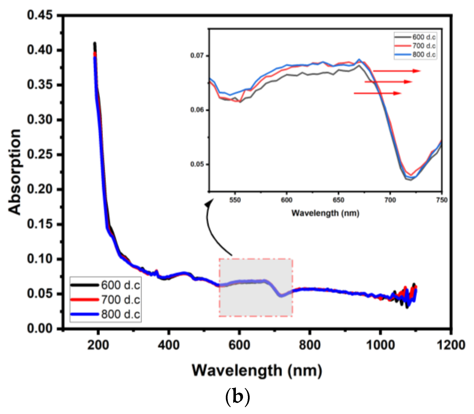
Photoluminescence is the light emission from any matter after photon absorption, also known as UV-Vis spectroscopy. This process involves the absorption of photons by a material, followed by re-emission of photons at lower energies with a smaller number of photons. Photoluminescence can be analyzed with the absorbance graph from UV-Vis data [40,41]. Figure 6 shows the absorbance peaks for both Si0.8Ge0.2 and Si0.9Ge0.1 shift towards the right side; this is observed as a red shift. These observations are consistent with the AFM data for Si0.8Ge0.2 and Si0.9Ge0.1 at 800 °C (74.5 nm and 97.7 nm, respectively). At high doping concentrations, the band gap for both Si0.8Ge0.2 and Si0.9Ge0.1 thin films is reduced due to the convergence of the donor and conduction bands; these are the effects of red shift in the optical absorption [42,43,44,45].

4. Conclusions

This study investigated the impact of annealing temperature on the structural and optical properties ofSi0.8Ge0.2 and Si0.9Ge0.1 compositions fabricated using RF sputtering. Both compositions exhibited significant changes in their optical properties, with Si0.8Ge0.2 showing greater variation than Si0.9Ge0.1. The transparency analysis revealed that the transparency of Si0.8Ge0.2 decreased with increasing temperature, while the transparency of Si0.9Ge0.1 remained constant at around 87.9%. The difference in transparency between the two compositions was found to be 0.1%. The structural stability of Si0.8Ge0.2 was attributed to its higher grain size and particle density when compared to Si0.9Ge0.1, which had lower values for these properties. Overall, Si0.9Ge0.1 was found to be the optimal composition in this study due to its higher transparency, larger grain size, and crystallite size at 800 °C. XRD and surface analysis revealed that SiGe nanostructure materials exhibited a larger bandgap than bulk crystals. These findings suggest that SiGe with a larger bandgap may be advantageous in ultraviolet photodetector applications.

Author Contributions

Conceptualization, B.K.G., F.P.C. and S.N.; methodology, S.N.; software, M.I.R.; validation, B.K.G., F.P.C. and M.D.; formal analysis, S.N.; investigation, S.N; resources, S.N.; data curation, R.R., F.J., M.I.R., M.D. and S.N.; writing—original draft preparation, S.N.; writing—review and editing, S.N.; visualization, R.R.; supervision, B.K.G. and F.P.C.; project administration, B.K.G.; funding acquisition, F.P.C. and B.K.G. All authors have read and agreed to the published version of the manuscript.

Funding

This research was funded by Ministry of Higher Education Fundamental Research Grant Scheme (FRGS/1/2020/STG07/UMS/02/1) and Universiti Malaysia Sabah (SDK0311-2020). The APC was funded by Universiti Malaysia Sabah.

Data Availability Statement

Not applicable.

Conflicts of Interest

The authors declare no conflict of interest.

References

  1. Goktas, S.; Goktas, A. A comparative study on recent progress in efficient ZnO based nanocomposite and heterojunction photocatalysts: A review. J. Alloy. Compd. 2021, 863, 158734. [Google Scholar] [CrossRef]
  2. Feng, X.; Sun, D.; Yang, J. Eco-friendly synthesis of ferric ion-polyphenol-graphene aerogel for solar steam generation. Mater. Lett. 2022, 313, 131738. [Google Scholar] [CrossRef]
  3. Tajima, K.; Qiu, F.; Shin, W.; Sawaguchi, N.; Izu, N.; Matsubara, I.; Murayama, N. Thermoelectric properties of RF-sputtered SiGe thin film for hydrogen gas sensor. Jpn. J. Appl. Phys. 2004, 43, 5978. [Google Scholar] [CrossRef]
  4. Ghosh, B.K.; Saad, I.; Teo KT, K.; Ghosh, S.K. mcSi and CdTe solar photovoltaic challenges: Pathways to progress. Optik 2020, 206, 164278. [Google Scholar] [CrossRef]
  5. Ferhati, H.; Djeffal, F. Role of non-uniform Ge concentration profile in enhancing the efficiency of thin-film SiGe/Si solar cells. Optik 2018, 158, 192–198. [Google Scholar] [CrossRef]
  6. Ali, A.; Cheow, S.L.; Azhari, A.W.; Sopian, K.; Zaidi, S.H. Enhancing crystalline silicon solar cell efficiency with SixGe1−x layers. Results Phys. 2017, 7, 225–232. [Google Scholar] [CrossRef]
  7. Hashemi, P.; Ando, T.; Balakrishnan, K.; Koswatta, S.; Lee, K.L.; Ott, J.A.; Mo, R.T. High performance PMOS with strained high-Ge-content SiGe fins for advanced logic applications. In Proceedings of the 2017 International Symposium on VLSI Technology, Systems and Application (VLSI-TSA), Hsinchu, Taiwan, 24–27 April 2017; IEEE: Piscataway, NJ, USA, 2017; pp. 1–2. [Google Scholar]
  8. Zhao, C.; Dong, Z.; Shen, J. The strain model of misfit dislocations at Ge/Si hetero-interface. Vacuum 2022, 196, 110711. [Google Scholar] [CrossRef]
  9. Masood, K.; Jain, N.; Kumar, P.; Malik, M.; Singh, J. Nanostructured thermoelectric Materials. In Thermoelectricity and Advanced Thermoelectric Materials; Elsevier: Amsterdam, The Netherlands, 2021; pp. 261–311. [Google Scholar]
  10. Ballif, C.; Haug, F.J.; Boccard, M.; Verlinden, P.J.; Hahn, G. Status and perspectives of crystalline silicon photovoltaics in research and industry. Nat. Rev. Mater. 2022, 7, 597–616. [Google Scholar] [CrossRef]
  11. Shukla, A.K.; Sudhakar, K.; Baredar, P. Simulation and performance analysis of 110 kWp grid-connected photovoltaic system for residential building in India: A comparative analysis of various PV technology. Energy Rep. 2016, 2, 82–88. [Google Scholar] [CrossRef]
  12. Dos Santos, R.B.; Rivelino, R.; de Brito Mota, F.; Kakanakova-Georgieva, A.; Gueorguiev, G.K. Feasibility of novel (H 3 C) n X (SiH 3) 3−n compounds (X = B, Al, Ga, In): Structure, stability, reactivity, and Raman characterization from ab initio calculations. Dalton Trans. 2015, 44, 3356–3366. [Google Scholar] [CrossRef]
  13. Tsukamoto, T.; Aoyagi, Y.; Nozaki, S.; Hirose, N.; Kasamatsu, A.; Matsui, T.; Suda, Y. Increasing the critical thickness of SiGe layers on Si substrates using sputter epitaxy method. J. Cryst. Growth 2022, 600, 126900. [Google Scholar] [CrossRef]
  14. Shklyaev, A.A.; Vdovin, V.I.; Volodin, V.A.; Gulyaev, D.V.; Kozhukhov, A.S.; Sakuraba, M.; Murota, J. Structure and optical properties of Si and SiGe layers grown on SiO2 by chemical vapor deposition. Thin Solid Film. 2015, 579, 131–135. [Google Scholar] [CrossRef]
  15. Ghosh, B.K.; Nasir, S.; Chee, F.P.; Routray, S.; Saad, I.; Mohamad, K.A. Numerical study of nSi and nSiGe solar cells: Emerging microstructure nSiGe cell achieved the highest 8.55% efficiency. Opt. Mater. 2022, 129, 112539. [Google Scholar] [CrossRef]
  16. Lahwal, A.; Zeng, X.; Bhattacharya, S.; Zhou, M.; Hitchcock, D.; Karakaya, M.; Tritt, T.M. Enhancing Thermoelectric Properties of Si80Ge20 Alloys Utilizing the Decomposition of NaBH4 in the Spark Plasma Sintering Process. Energies 2015, 8, 10958–10970. [Google Scholar] [CrossRef]
  17. Wu, Y.H.; Chen, W.J.; Chin, A.; Tsai, C. The effect of native oxide on epitaxial SiGe from deposited amorphous Ge on Si. Appl. Phys. Lett. 1999, 74, 528–530. [Google Scholar] [CrossRef]
  18. Goktas, A.; Aslan, E.; Arslan, F.; Kilic, A. Characterization of multifunctional solution-processed Sn1-xZnxS nanostructured thin films for photosensitivity and photocatalytic applications. Opt. Mater. 2022, 133, 112984. [Google Scholar] [CrossRef]
  19. Li, Y.; Han, J.; Xiang, Q.; Zhang, C.; Li, J. Enhancing thermoelectric properties of p-type SiGe by SiMo addition. J. Mater. Sci. Mater. Electron. 2019, 30, 9163–9170. [Google Scholar] [CrossRef]
  20. Abidin, M.S.Z.; Morshed, T.; Chikita, H.; Kinoshita, Y.; Muta, S.; Anisuzzaman, M.; Park, J.H.; Matsumura, R.; Mahmood, M.R.; Sadoh, T.; et al. The Effects of Annealing Temperatures on Composition and Strain in Si x Ge1− x Obtained by Melting Growth of Electrodeposited Ge on Si (100). Materials 2014, 7, 1409–1421. [Google Scholar] [CrossRef]
  21. Zhu, J.; Liu, S.; Yang, S.; Zhang, Y.; Zhang, J.; Zhang, C.; Deng, C. The Effect of Different Annealing Temperatures on Recrystallization Microstructure and Texture of Clock-Rolled Tantalum Plates with Strong Texture Gradient. Metals 2019, 9, 358. [Google Scholar] [CrossRef]
  22. Zhang, Z.; Zhang, Y.; Mishin, O.V.; Tao, N.; Pantleon, W.; Juul Jensen, D. Microstructural Analysis of Orientation-Dependent Recovery and Recrystallization in a Modified 9Cr-1Mo Steel Deformed by Compression at a High Strain Rate. Metall. Mater. Trans. A 2016, 47, 4682–4693. [Google Scholar] [CrossRef]
  23. Mohamed, M.; Sedky, A.; Kassem, M.A. Gradual growth of ZnO nanoparticles from globules-like to nanorods-like shapes: Effect of annealing temperature. Optik 2022, 265, 169559. [Google Scholar] [CrossRef]
  24. Sharma, M.; Rani, J.; Bhardwaj, S.; Agrawal, A.; Ghosh, R.K.; Kuanr, B.K. Effect of annealing temperature on structural, optical, magnetic and electrical properties of CrFeO3 multiferroic nanoparticles: A validation to first-principle calculations. J. Alloys Compd. 2022, 929, 167338. [Google Scholar] [CrossRef]
  25. Bruker, C. NanoScope Software 8.10 User Guide. [online] Nanoqam.ca. 2011. Available online: http://nanoqam.ca/wiki/lib/exe/fetch.php?media=nanoscope_software_8.10_user_guide-d_004-1025-000_.pdf (accessed on 7 October 2022).
  26. Kama, A.; Tirosh, S.; Itzhak, A.; Ejgenberg, M.; Cahen, D. New Pb-Free Stable Sn–Ge Solid Solution Halide Perovskites Fabricated by Spray Deposition. ACS Appl. Energy Mater. 2022, 5, 3638–3646. [Google Scholar] [CrossRef]
  27. Torimoto, T.; Kameyama, T.; Uematsu, T.; Kuwabata, S. Controlling Optical Properties and Electronic Energy Structure of I-III-VI Semiconductor Quantum Dots for Improving Their Photofunctions. J. Photochem. Photobiol. C Photochem. Rev. 2022, 54, 100569. [Google Scholar] [CrossRef]
  28. El-Denglawey, A.; Sharma, V.; Sharma, E.; Aly, K.A.; Dahshan, A.; Sharma, P. Optical and mechanical properties of Ag doped thermally evaporated SeTe thin films for optoelectronic applications. J. Phys. Chem. Solids 2021, 159, 110291. [Google Scholar] [CrossRef]
  29. Dash, P.K.; Gupta, N.C. Effect of temperature on power output from different commercially available photovoltaic modules. Int. J. Eng. Res. Appl. 2015, 5, 148–151. [Google Scholar]
  30. Mohammed, R.Y. Annealing Effect on the Structure and Optical Properties of CBD-ZnS Thin Films for Windscreen Coating. Materials 2021, 14, 6748. [Google Scholar] [CrossRef]
  31. Özen, S.; Pat, S.; Şenay, V.; Korkmaz, Ş.; Geçici, B. Some physical properties of the SiGe thin film coatings by thermionic vacuum arc (TVA). J. Nanoelectron. Optoelectron. 2015, 10, 56–60. [Google Scholar] [CrossRef]
  32. Markvart, T.; Castañer, L. Semiconductor materials and modeling. In McEvoy’s Handbook of Photovoltaics; Academic Press: Cambridge, MA, USA, 2018; pp. 29–57. [Google Scholar]
  33. Shen, L.; Zhang, X.; Wang, H.; Li, J.; Xiang, G. Structural, magnetic and Magneto-transport properties of Mn-doped SiGe thin films. J. Magn. Magn. Mater. 2022, 560, 169630. [Google Scholar] [CrossRef]
  34. Nguyen, V.H.; Novikov, A.; Shaleev, M.; Yurasov, D.; Semma, M.; Gotoh, K.; Usami, N. Impact of Ge deposition temperature on parameters of c-Si solar cells with surface texture formed by etching of Si using SiGe islands as a mask. Mater. Sci. Semicond. Process. 2020, 114, 105065. [Google Scholar] [CrossRef]
  35. Saikumar, A.K.; Sundaresh, S.; Nehate, S.D.; Sundaram, K.B. Properties of RF magnetron-sputtered copper gallium oxide (CuGa2O4) thin films. Coatings 2021, 11, 921. [Google Scholar] [CrossRef]
  36. Cojocaru, O.; Lepadatu, A.M.; Nemnes, G.A.; Stoica, T.; Ciurea, M.L. Bandgap atomistic calculations on hydrogen-passivated GeSi nanocrystals. Sci. Rep. 2021, 11, 1–10. [Google Scholar] [CrossRef]
  37. Marsili, M.; Botti, S.; Palummo, M.; Degoli, E.; Pulci, O.; Weissker, H.C.; Del Sole, R. Ab initio electronic gaps of Ge nanodots: The role of self-energy effects. J. Phys. Chem. C 2013, 117, 14229–14234. [Google Scholar] [CrossRef]
  38. Bulutay, C. Interband, intraband, and excited-state direct photon absorption of silicon and germanium nanocrystals embedded in a wide bandgap lattice. Phys. Rev. B 2007, 76, 205321. [Google Scholar] [CrossRef]
  39. Peng, K.C.; Kao, H.C.; Liu, S.J.; Tsai, K.L.; Lin, J.C. Annealing effect on the microstructure and optical characterization of Zn2SiO4 thin film sputtered on quartz glass. Jpn. J. Appl. Phys. 2013, 52, 11NB04. [Google Scholar] [CrossRef]
  40. Baer, D.R.; Thevuthasan, S. Characterization of thin films and coatings. In Handbook of Deposition Technologies for Films and Coatings; William Andrew Publishing: Norwich, NY, USA, 2010; pp. 749–864. [Google Scholar]
  41. Supriyanto, A.; Ramelan, A.H.; Nurosyid, F. Effect of annealing temperature on optical properties of TiO2 18 NR-T type thin film. J. Phys. Conf. Ser. 2018, 1011, 12016. [Google Scholar]
  42. Tang, G.; Liu, H.; Zhang, W. The variation of optical band gap for ZnO: In films prepared by sol-gel technique. Adv. Mater. Sci. Eng. 2013, 2013, 348601. [Google Scholar] [CrossRef]
  43. Elmorsy, M.R.; Badawy, S.A.; Abdel-Latif, E.; Assiri, M.A.; Ali, T.E. Significant improvement of dye-sensitized solar cell performance using low-band-gap chromophores based on triphenylamine and carbazole as strong donors. Dye. Pigment. 2023, 214, 111206. [Google Scholar] [CrossRef]
  44. Fathipour, M.; Abbaszadeh, B.; Kohani, F.; Farbiz, F. The effect of GE mole fraction on the electrical characteristics of nanoscale Si/SiGe heterostructure pMOSFET. In 2007 International Semiconductor Device Research Symposium; IEEE: Piscataway, NJ, USA, 2007; pp. 1–2. [Google Scholar]
  45. John, K.I.; Obu, M.; Adeleye, A.T.; Ebiekpe, V.; Adenle, A.A.; Chi, H.; Omorogie, M.O. Oxygen deficiency induction and boundary layer modulation for improved adsorption performance of titania nanoparticles. Chem. Pap. 2022, 76, 3829–3840. [Google Scholar] [CrossRef]
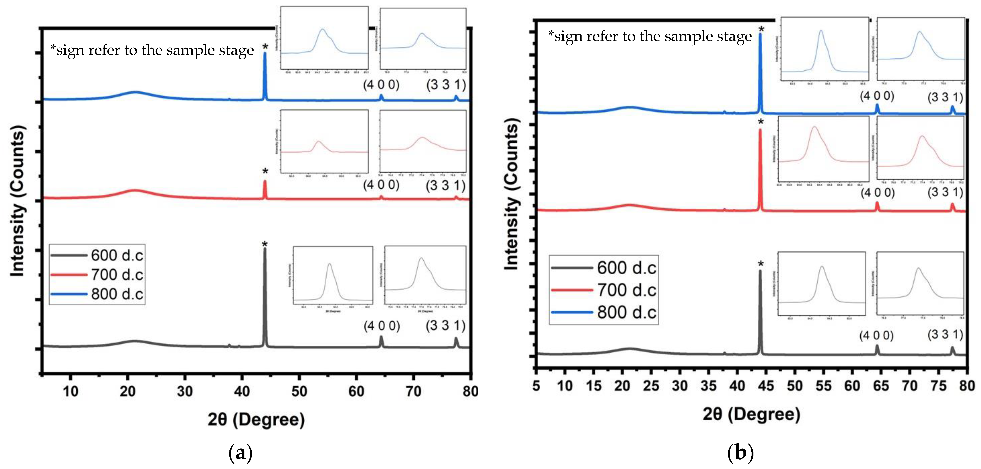
Figure 1. XRD result for both (a) Si0.8Ge0.2 and (b) Si0.9Ge0.1 composition.
Crystals 13 00791 g001
Figure 2. AFM analysis for both crystalline Si0.8Ge0.2 at (a) 600 °C, (b) 700 °C, and (c) 800 °C, and Si0.9Ge0.1 (d) 600 °C, (e) 700 °C, and (f) 800 °C.
Crystals 13 00791 g002
Figure 3. The crystallite size and RMS roughness graph against annealing temperature for both (a) Si0.8Ge0.2 and (b) Si0.9Ge0.1.
Crystals 13 00791 g003
Figure 4. Transmittance graph for (a) Si0.8Ge0.2 and (b) Si0.9Ge0.1 at 600 °C, 700 °C and 800 °C.
Crystals 13 00791 g004
Figure 5. The energy vs. (ahv)2, band gap graph for (a) Si0.8Ge0.2 and (b) Si0.9Ge0.1 composition.
Crystals 13 00791 g005
Figure 6. Absorbance shifts for (a) Si0.8Ge0.2 and (b) Si0.9Ge0.1 thin film.
Crystals 13 00791 g006aCrystals 13 00791 g006b
Table 1. Deposition composition and parameters.
Thin Film Composition
  • Silicon Germanium (Si 90%, Ge 10%) wt%
  • Silicon Germanium (Si 80%, Ge 20%) wt%
Material purity (Sputter target)99.99%
Target size3″ diameter × 0.125″ thickness
SubstrateQuartz Glass
Annealing temperature600 °C, 700 °C and 800 °C
Sputtering power98 W
Table 2. The structural properties for XRD data.
CompositionSi0.8Ge0.2Si0.9Ge0.1
ParameterCrystallite Size (nm)Micro-Strain, ×10−3 (Rad)Lattice ConstantPeak PositionCrystallite Size (nm)Micro-Strain, ×10−3 (radian)Lattice ConstantPeak Position
600 °C35.791.925.5800264.4°, 77.5°35.631.915.5793264.4°, 77.5°
700 °C31.41143.765.5808664.4°, 77.5°22.981.925.5810264.4°, 77.5°
800 °C36.78165.495.5805764.4°, 77.5°36.280.975.5806364.4°, 77.5°
Table 3. The summary of structural properties for both SiGe compositions using AFM analysis.
CompositionSi0.8Ge0.2Si0.9Ge0.1
ParameterGrain Size (nm)RMS Roughness (nm)Particle Density (µm−2)Grain Size (nm)RMS Roughness (nm)Particle Density (µm−2)
600 °C61.07820.319.96169.35923.924.897
700 °C70.89528.651.40187.97834.717.889
800 °C74.86826.452.48697.68927.719.868
Table 4. The summary of transmittance at 850 nm wavelength and bandgap for both SiGe compositions from the absorption graph.
CompositionSi0.8Ge0.2Si0.9Ge0.1
Optical ParameterTransmittance (%)Bandgap (eV)Transmittance (%)Bandgap (eV)
600 °C87.875.50587.95.528
700 °C86.865.38087.95.558
800 °C87.285.59587.95.429
Disclaimer/Publisher’s Note: The statements, opinions and data contained in all publications are solely those of the individual author(s) and contributor(s) and not of MDPI and/or the editor(s). MDPI and/or the editor(s) disclaim responsibility for any injury to people or property resulting from any ideas, methods, instructions or products referred to in the content.