Abstract
As the size of SiC crystals gradually increase, it becomes increasingly difficult to control the temperature distribution inside the crucible. In this study, numerical simulation tools were used to model the thermal field of SiC single crystal growth using the resistance heating PVT method. Through adjusting the relative position of the heater, adjusting the crucible and insulation structure, and setting up dual heaters, the temperature field distribution patterns under different conditions were obtained. The research results indicate that adjusting the relative positions of the heater, the crucible and insulation structure can achieve uniform temperature conditions under specific conditions. The use of dual heaters can achieve ideal crystal growth conditions with a growth interface temperature difference of less than 10 K, and an axial temperature gradient magnitude of about 10 K/cm, with a smaller edge axial temperature gradient, which is helpful to avoid edge polycrystalline formation and improve crystal quality. Meanwhile, combined with the top insulation layer, more energy-saving effects can be achieved, providing a reference for the preparation of large-sized SiC crystals.
1. Introduction
Silicon carbide (SiC) is a promising new electronic material with excellent physical and chemical properties. Compared with silicon-based electronic devices, electronic devices based on SiC substrates stand out on the surface in high-voltage, high-frequency, high-power, and harsh environmental scenarios, and have broad application prospects in emerging fields, such as new energy vehicles, power generation and storage, rail transit, smart grids, and radio frequency communication. Especially in the context of low-carbon and green development today, the demand for SiC power devices is rapidly increasing, and their large-scale applications are believed to bring about a revolution in the power electronics industry [1,2]. However, the high cost of SiC devices limits their application for a large scale, with substrate costs accounting for 47% of device costs. Therefore, a decrease in substrate costs is imperative.
The preparation of large-sized SiC single crystals has always been the focus of research in the field. The mainstream preparation method for SiC single crystals is the PVT method [3]. Usually, the seed crystal and raw materials are placed at the top and bottom of the crucible, respectively. Under low pressure conditions, a suitable temperature distribution is formed inside the crucible. With a high temperature, the gas-phase components generated through powder decomposition are transported to the surface of the seed crystal under the action of temperature gradients, achieving crystal growth [4,5,6]. Temperature distribution plays an extremely important role in the crystal growth process. In 1990, Cree Company used the PVT method to grow 25 mm diameter SiC single crystals. Subsequently, the company began promoting the commercialization of materials, and by 2022, individual units in China had successfully prepared 200 mm diameter SiC single crystals [7]. However, the 200 mm diameter SiC single crystal substrate is still in the early stage of industrialization, and there is still a significant gap in crystal quality and thickness compared to 6-inch SiC. For decades, people have adopted many methods to improve crystal quality and size [8,9,10], including using seed crystals with a certain angle to better meet the requirements of step flow growth mode and reduce the number of defects, using different seed crystal fixation methods to reduce stress caused by different thermal expansion coefficients between materials and graphite [11,12], and adopting different materials and structures to optimize the internal environment of the chamber [13,14,15]. Some researchers studied dislocation formation and found that the largest dislocation density is focused near the graphite and SiC interface [16]. Using different seed bonding methods to reduce crystal stress is also one of the methods to improve crystal quality [17]. There are also studies [18,19] that have characterized the morphology and characteristics of defects in detail, which is beneficial for analyzing the mechanism of defect formation. Due to the need for high-quality crystal growth to maximize the consistency of different regions on the growth interface, improving crystal growth conditions through thermal field design and optimization has always been a popular topic of concern for researchers [20,21,22]. However, the existing research mainly focuses on traditional induction heating equipment [21,23]. Induction heating and resistance heating have different heat transfer characteristics. The former has the advantage of a high-energy-conversion efficiency, but the induction coil is usually circular, which brings certain limitations to the thermal field optimization [24,25]. The resistance heating method, on the other hand, can better design the required temperature range due to the separation of the heater and the crucible, demonstrating its potential advantages in large-sized crystal growth. However, the temperature distribution on the surface of crystal growth has a direct impact on crystal quality, and as the crystal size increases, the difficulty of controlling the temperature at the growth interface becomes greater, which poses a great challenge to the quality control of large-sized crystal growth.
In summary, the key to the growth of SiC single crystals lies in the design of temperature conditions, especially the regulation of radial temperature consistency and axial temperature gradient at the growth interface as the crystal size increases. How to achieve a large axial temperature gradient distribution with small edges and large centers, while obtaining a uniform temperature distribution, is an important direction for temperature field optimization. However, crystal growth requires high-temperature conditions above 2300 °C, making it difficult to directly and effectively monitor [26]. In this article, COMSOL 6.0 software was used to simulate the thermal field of resistance-heated, 204 mm diameter SiC single crystal preparations. The electromagnetic heating, non-isothermal flow, and heat transfer processes were analyzed, and the temperature distribution characteristics under basic conditions were obtained. Through adopting structural optimization and a dual heater design, a better temperature distribution was obtained, providing useful references for the research and industrialization of large-sized SiC crystal growth under resistance heating conditions.
2. Experimental
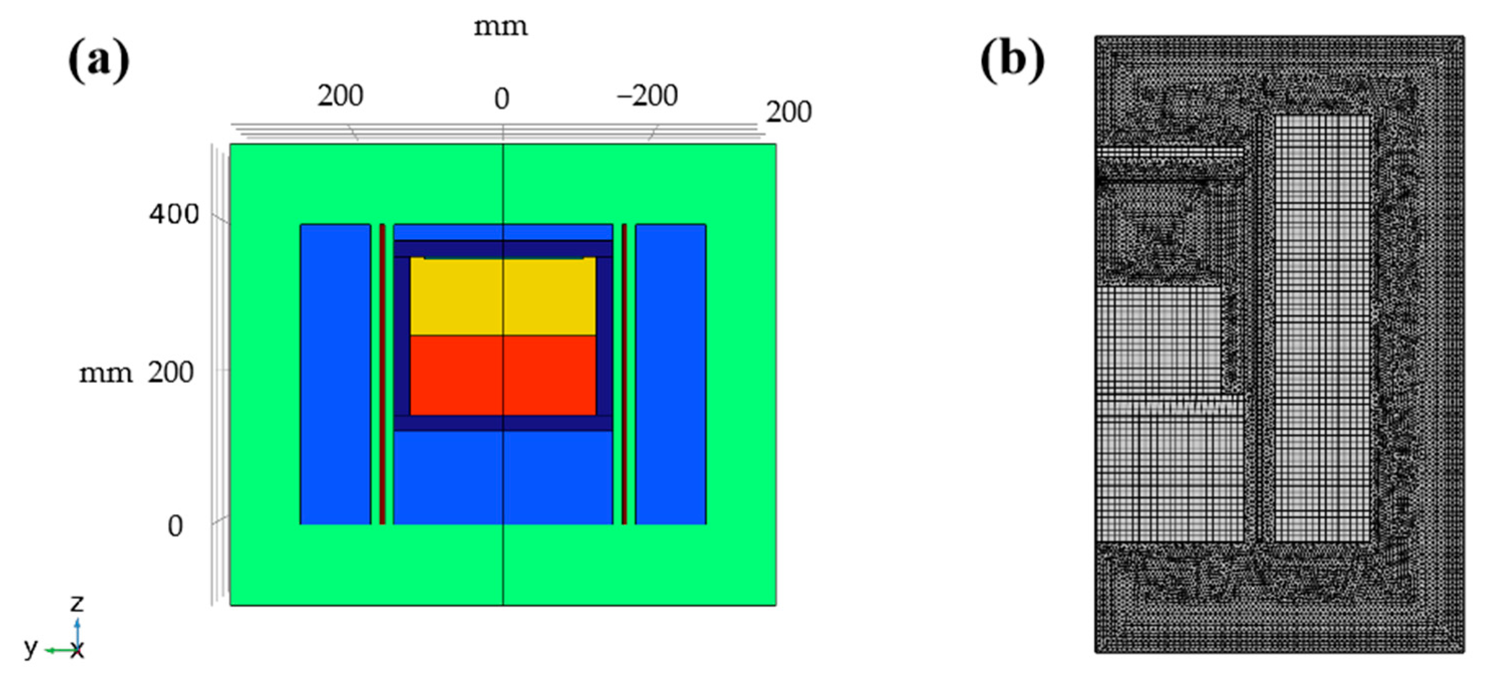
The growth of SiC crystals occurs in a high-temperature device in the equipment, as shown in Figure 1. The thermal field structure is located at the center of the device, surrounded by graphite soft felt with minimal thermal conductivity and cylindrical graphite heaters. The internal structure of the thermal field includes insulation materials on the upper and lower parts as supportation, as well as a graphite crucible in the middle. From top to bottom, the graphite crucible contains SiC seed crystals, growth chambers, and raw materials. The entire device is a central axis symmetric structure, which can effectively simplify the calculation. The main structural parameters are shown in Table 1. During the crystal growth process, the SiC raw material is in a relatively high-temperature zone and the seed crystal is in a relatively low-temperature zone, which promotes the sublimation and decomposition of the raw material and directly generates gas-phase SixCy substances (mainly including Si, Si2C, SiC2, etc.) without going through the liquid phase. These gas-phase substances nucleate and grow at the C face of seed crystal, forming SiC single crystals [3]. The temperature gradient from the surface of the raw material to the seed crystal is the driving force for the crystal growth. Usually, the designed temperature gradient is between 5 and 20 K/cm. The higher the temperature gradient, the higher the supersaturation of the gas-phase material reaching the seed crystal surface, and the faster the growth rate of SiC crystals [24].
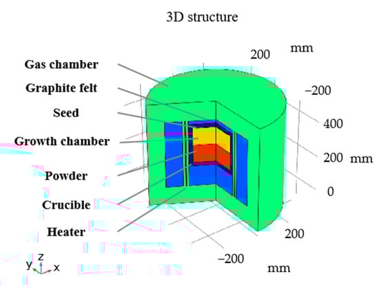
Figure 1.
Structure of SiC crystal growth thermal field.

Table 1.
The geometric dimensions of the thermal field.
In the device, both the crucible and the heater are made of high-purity graphite. The insulation materials at the top and bottom of the crucible, as well as the insulation materials around the heater, are made of graphite soft felt. The raw material is SiC powder, and the gas is argon. The gas pressure is set to 2000 Pa. The basic physical parameters of the relevant materials are shown in Table 2 [27,28]. It should be pointed out that due to the fact that the actual heater is a thin cylindrical structure with gaps, the thermal conductivity of the graphite material used in the heater has been adjusted to 1/10 of the theoretical parameters based on the shape of the heater. The detailed description of the correlation function can be found in the supplementary electronic materials.
Table 2.
The specifications of the relevant materials.
Different regions of the device adopt different grid-partitioning strategies based on computational demands. The seed crystal, heater, growth chamber, crucible, and gas chamber use unstructured grids with a minimum cell size of 0.05 mm. The shape of the powder and graphite felt is relatively regular, using a structured grid with a maximum unit size of 6 mm. In Figure 2, the structural schematic diagram after grid division is shown. Finally, the complete grid contains 8440 domain elements and 868 boundary elements, including 6402 triangular elements and 2038 quadrilateral elements, with an average unit mass of 0.9022, indicating good grid quality.

Figure 2.
Device 2D profile and typical grid. (a) Device profile. (b) Divided grid.
The principle of resistance heating is to heat a thermal field device through the Joule heating effect of current. Due to static and low-frequency conditions, there is no need to consider magnetic fields, and the current and potential of the heater are calculated based on Ohm’s law. During the simulation, only the steady-state value of the thermal field under given conditions is considered as a steady-state calculation. For the gas in the growth chamber, due to the low gas pressure and ignoring the influence of turbulence, the gas flow can be considered as laminar and compressible, taking into account the factor of gravity. Under high-temperature conditions, over 2000 °C in the growth chambers, radiation heat transfer becomes an important heat transfer method that cannot be ignored, so the surface and surface radiation on the surface of high-temperature objects is calculated. For the entire device, the external boundary is usually a water-cooled shell, which is set at 300 K in the model.
The heat inside the device originates from the Joule heating effect of the heater, and in the model, the required current is obtained through setting the electric potential of the heater. In the calculation process, in order to improve the stability of the calculation, auxiliary scanning is used to set different potentials from small to large for solving. During the calculation process, a potential is applied to the top of the heater and the bottom of the heater is grounded. The temperature distribution under different conditions is calculated and compared with the experimental device. Under initial conditions, the potential is set to 20 V. During the optimization design process, adjustments were made to the shape of the crucible and insulation structure, as well as to the length and number of heaters. Meanwhile, the material parameters and physical processes remained unchanged for comparison.
3. Results and Discussion
3.1. Characteristics of Temperature and Flow Field Distribution under a Basic Thermal Field
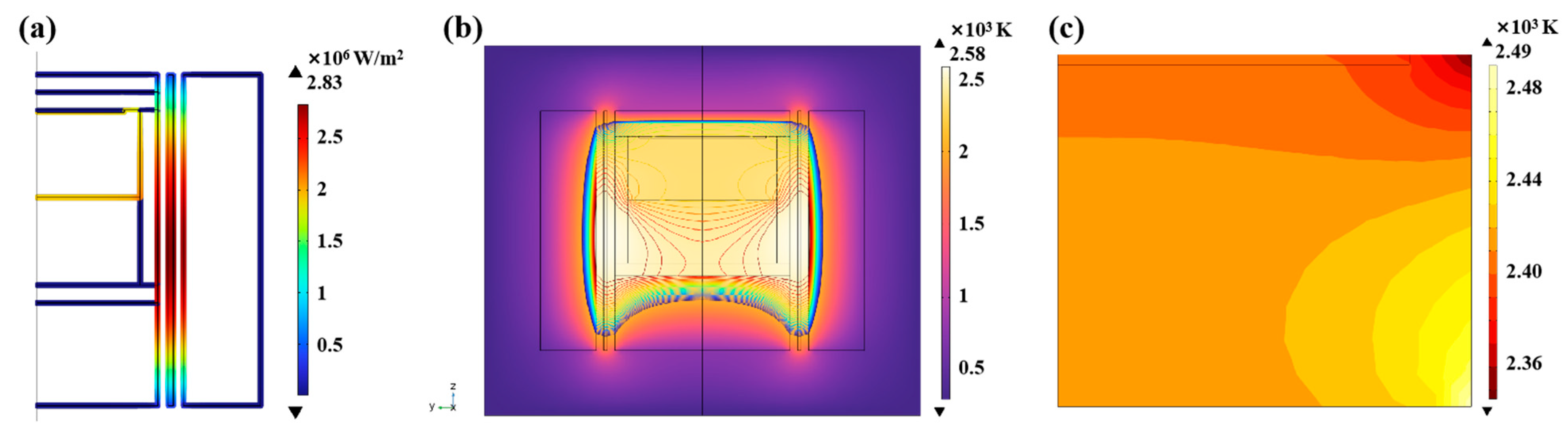
The calculated results for analysis were visualized. Figure 3 shows the boundary radiance and temperature distribution within the device. The radiance of each wall surface describes the radiation flux at that location. The cylindrical resistance heater serves as the heating source, and the middle section has the maximum parameter, reaching 2.8 MW/m2. It rapidly decays with distance, and still reaches over 2 MW/m2 on the inner wall of the crystal growth chamber and the surface of the raw material. The temperature distribution in the device is basically consistent with the radiation distribution, and the high-temperature zone is located in the middle section of the heater. This is because the raw material at the bottom of the crucible has a greater heat transfer coefficient compared to the gas, which also presents a temperature gradient from bottom to top inside the crucible. The highest temperature in the device reaches 2580 K, and the lowest temperature is located at the edge of the side insulation layer, with a temperature around 1000 K. The temperature distribution inside the growth chamber is labeled with different colors, with a difference of 10 K between adjacent color blocks. There are maximum and minimum temperature values at the bottom and top edges of the growth chamber, respectively, with a temperature difference of 140 K. However, the temperature difference between the seed crystal and the raw material is within 20 K, indicating that under basic thermal field conditions, there is a problem of a large radial temperature difference between the seed crystal and a too-small overall temperature gradient.
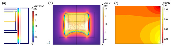
Figure 3.
Radiance and temperature distribution (a) Radiance (b) Thermal field temperature distribution (c) Growth chamber temperature distribution.
Affected by the high temperature at the edge of the crucible, there is convection in the gas inside the growth chamber. Without considering the decomposition and gasification of raw materials, the gas flow distribution is shown in Figure 4. The gas moves upwards along the inner wall of the growth chamber, then towards the center of the seed crystal, and then reaches the surface of the raw material and continues to move towards the inner wall. The maximum flow rate reaches 0.0075 m/s. Figure 4b,c, respectively, shows the contour cloud and stereo images of the axial and radial velocity of gas in the growth chamber. There is a maximum upward airflow near the wall of the growth chamber, which means that the components formed through raw material decomposition will be preferentially replenished to the edge of the growth interface. There is a maximum downward airflow near the center of the growth chamber, which means that a large number of gas-phase components are transported to the surface of the raw material. This law is completely consistent with the fast growth rate of seed crystal edges during the crystal growth process, which makes it easy to form polycrystals, and the easy occurrence of recrystallization on the surface of raw materials, which must be considered in the thermal field design.
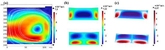
Figure 4.
Velocity distribution in the growth chamber (a) Velocity magnitude (Arrows indicate the direction of gas flow) (b) Axial velocity (c) Radial velocity.
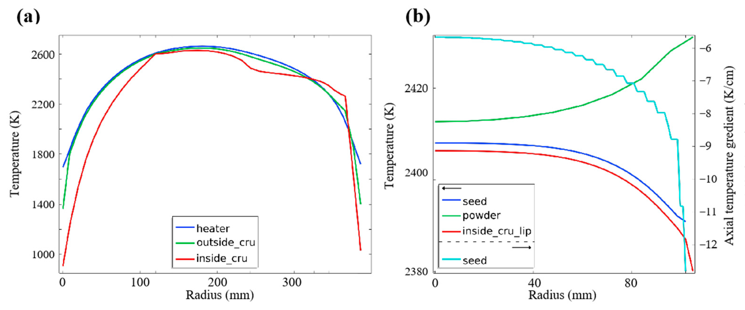
The temperature distribution at different boundaries under basic thermal field conditions is shown in Figure 5. Figure 5a shows the temperature distribution of the inner wall of the heater, the outer wall of the crucible, and the inner wall of the crucible. Due to the close distance between the heater and the crucible, radiation heat transfer dominates, and the temperature difference between the inner and outer walls of the crucible is affected by the material inside the crucible. From bottom to top, it shows a characteristic of first increasing and then decreasing. As shown in Figure 5b, the temperature difference between the seed crystal and the raw material has increased from around 10 K at the center to around 40 K at the edge, with a significant difference. At the same time, the axial temperature gradient at the growth interface decreased from −6 K/cm to −12 K/cm. The temperature of the seed crystal itself decreases from 2407 K in the central region to around 2390 K. It is necessary to optimize the graphite structure to reduce the radial temperature difference and improve the uniformity of the axial temperature gradient.
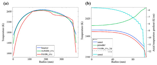
Figure 5.
Boundary temperature distribution. (a) Side-wall temperature distribution. (b) Horizontal-boundary temperature distribution.
3.2. Influence of Structural Adjustment on Temperature Uniformity
Due to the lower edge temperature of the seed crystal compared to the central region, the radial temperature distribution was optimized through structural adjustment, as shown in Figure 6. Different schemes were adopted to increase the edge temperature of seed crystals. On the basis of the basic thermal field, Figure 6b extends the length of the heater and side insulation by 30 mm. Figure 6c further adds a 30 mm high and 210 mm inner diameter insulation soft felt at the top edge of the crucible. It is expected to improve the temperature uniformity of the crystal surface through starting with the edge heater and insulation layer.
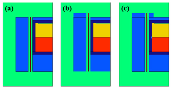
Figure 6.
Structural adjustment schemes (a) Scheme A (b) Scheme B (c) Scheme C.
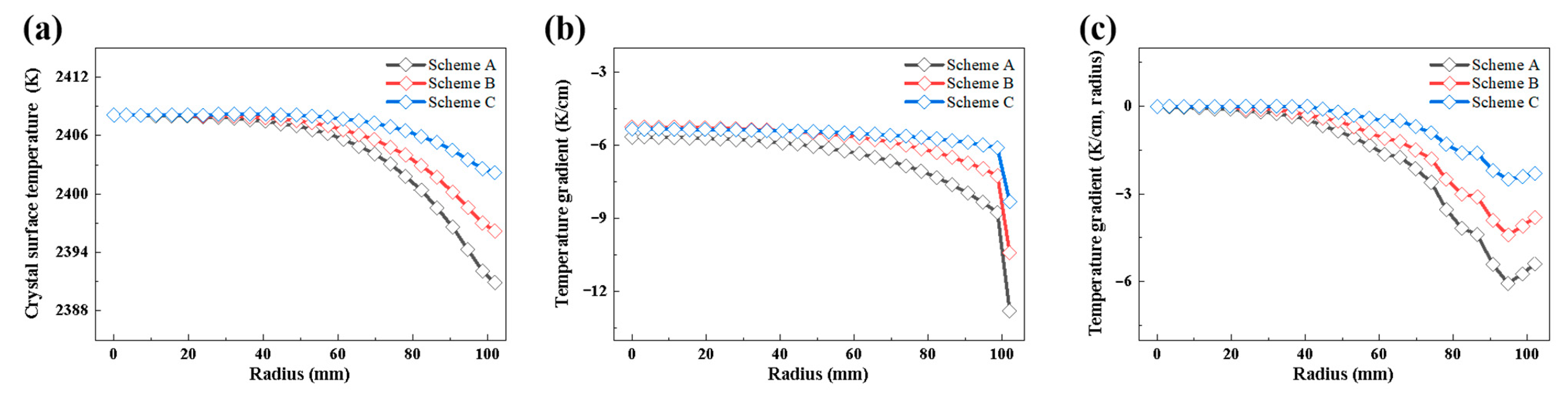
Figure 7 shows the radial temperature and temperature gradient along the seed crystal growth interface. Under the condition of keeping the center temperature of the seed crystal constant, extending the heater and installing an edge insulation layer can significantly increase the edge temperature of the seed crystal, with the edge temperature of the seed crystal increasing by 5 K and 6 K, respectively. At the same time, the axial temperature gradient under three conditions is between −5 and 13 K/cm2. Among them, after extending the heater and installing the edge insulation layer, the difference in temperature gradient along the radial axis of the seed crystal gradually decreases. This also verifies the improvement effect of increasing side heating and insulation on the temperature uniformity of the crystal surface. However, the drastic change in axial temperature gradient at the edge of the seed crystal suggests that polycrystalline deposition may be easily formed there. The radial temperature gradient on the crystal surface also reflects the difference in surface temperature of the seed crystal. The consistency is good in the central region of the crystal surface, with a radial temperature gradient around 0 and a minimum value near the edge of the seed crystal. This is because the side of the seed crystal is exposed and is affected by radiation heat transfer from the crucible side wall, resulting in a decrease in temperature drop in local areas. This indicates that simply adjusting the side insulation layer can achieve good temperature uniformity, but the increase in edge temperature significantly increases the axial temperature gradient, which is not conducive to the growth of low stress crystals at the micro-convex interface.
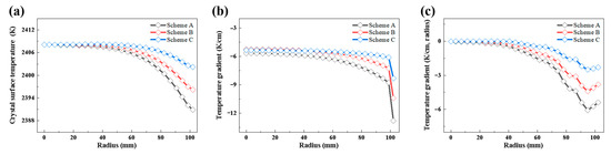
Figure 7.
Temperature and temperature gradient of the seed surface (a) Surface temperature (b) Vertical temperature gradient (c) Radial temperature gradient.
Due to the positive effect of extending the heater on increasing the edge temperature, further research was conducted on the basis of extending the heater. Through adjusting the thickness of the top insulation layer, the effect of top insulation on the growth interface temperature was compared. As shown in Figure 8, there are schemes for top insulation layers with different thicknesses. The thicknesses of top insulation layers for schemes D, E, and F are 33 mm, 24 mm, and 10 mm, respectively. Other parameters such as structure and heater input voltage were unchanged.
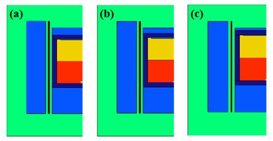
Figure 8.
Structural adjustment schemes (a) Scheme D (b) Scheme E (c) Scheme F.
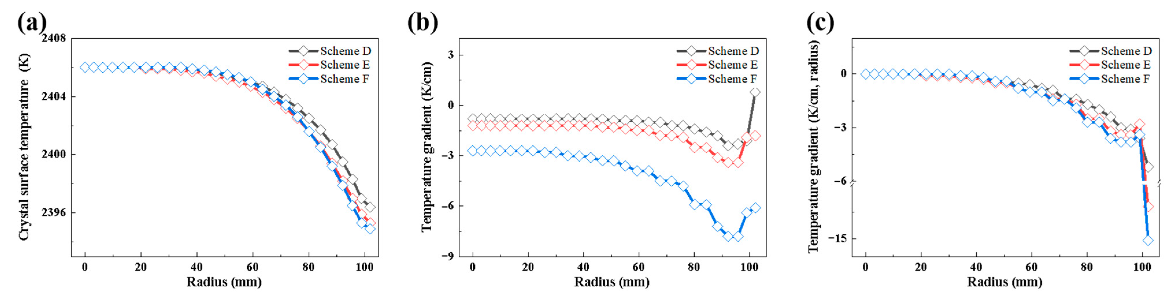
The temperature distribution of the growth interface is shown in Figure 9. Under this condition, the surface temperature difference of the seed crystal is about 11 K, and as the thickness of the top insulation layer decreases, the temperature at the edge of the growth interface gradually decreases. The absolute value of the radial temperature gradient rapidly increases as the thickness of the top insulation layer decreases, from about −2 K/cm at 30 mm to over −5 K/cm, indicating that the temperature gradient of the growth interface can be adjusted via the thickness of the top insulation layer. The axial temperature gradient undergoes significant changes between 24 mm and 10 mm, as the temperature gradient at the crystal growth interface gradually decreases with the increase of the thickness of the top insulation. When the thickness of the top insulation layer reaches 33 mm, due to the good insulation performance of the insulation soft felt, the internal temperature of the crucible is approximately uniformly distributed, which also provides the possibility for the construction of the temperature distribution required for crystal annealing. However, the thinning of the top insulation layer can cause a decrease in temperature gradient uniformity, which requires structural optimization to obtain an appropriate temperature gradient size and achieve good uniformity.
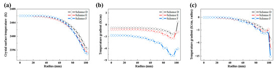
Figure 9.
Temperature and temperature gradient of the seed surface. (a) Surface temperature. (b) Vertical temperature gradient. (c) Radial temperature gradient.
3.3. Improving Temperature Field Distribution Using Dual Heaters
The above analysis shows that simply enhancing the top insulation is beneficial for improving radial temperature uniformity, but it is not conducive to obtaining a suitable axial temperature gradient. Extending the heater length is beneficial for improving the problem of low temperature at the edge of the crystal growth interface. Further strengthening the top-side insulation is beneficial for reducing the axial temperature gradient at the edge of the growth interface. However, relying on structural adjustment to optimize the uniformity of the crystal growth interface has certain limitations. Figure 10 shows different structural design schemes under dual-heater design conditions. All three schemes add a top heater on top of the crucible. Among them, the top of the heater on the side of scheme H is flush with the height of the seed crystal, and the top insulation layer is suspended above the top heater, with a certain gap between it and the side insulation layer. Scheme I extends the length of the side heater to match the top of the crucible, with the top insulation layer directly connected to the side insulation layer. Scheme J further sets up an ultra-thin graphite structure on the side of the seed crystal on the basis of Scheme I, forming a local gas cavity.
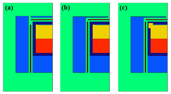
Figure 10.
Structural adjustment schemes (a) Scheme H (b) Scheme I (c) Scheme J.
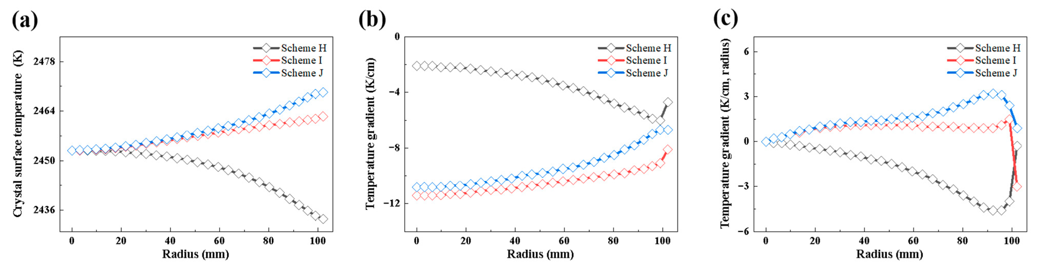
Under the condition of dual heaters, the temperature distribution at the crystal growth interface is shown in Figure 11. Under the same central temperature of the growth interface, the seed crystal edge temperature of the three schemes gradually increases and is higher than the central region temperature. At the same time, the axial temperature gradient on the surface of the seed crystal rapidly changes from −4 K/cm to −8–10 K/cm, which is conducive to maintaining a higher crystal growth rate. Unlike other schemes, using dual heaters, Scheme I and Scheme J achieved the effect of a large center gradient and a small edge temperature gradient, with the latter changing more significantly. This indicates that the growth rate of the growth interface edge is lower than the center position under this condition, which is conducive to the growth morphology of micro-convex crystals, avoiding polycrystalline growth caused through excessive edge growth, and reducing crystal cracking caused by edge polycrystals. The radial temperature gradient diagram of the growth interface shows that Scheme I and Scheme J are generally positive, with most of them located within 3 K/cm. Due to the influence of the top insulation layer structure, in the area near the edge of the seed crystal, Scheme H shows a different trend of change. Compared with Scheme I, Scheme J enhances the heat transfer effect in this area due to the thin inner wall of the crucible on the outer side of the seed crystal, resulting in a higher temperature at the edge of the crystal growth interface than the former, while the absolute value of the temperature gradient is lower than the former, providing different crystal growth conditions, which also provides more possibilities for regulating the SiC crystal growth rate.
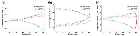
Figure 11.
Temperature and temperature gradient of the seed surface. (a) Surface temperature. (b) Vertical temperature gradient. (c) Radial temperature gradient.
In order to compare the temperature characteristics under different schemes, the temperature difference at the crystal growth interface and the required power per unit temperature under similar temperature conditions are shown in Figure 12. Scheme C has the smallest radial temperature difference, followed by Scheme D and Scheme I, because Scheme C further increases the temperature of the area through strengthening the insulation at the edges, while Scheme D has the maximum thickness of the top insulation layer. However, although the first two schemes have better temperature uniformity, there are different issues with temperature gradient distribution. The utilization efficiency of power under different schemes were compared through dividing the average temperature of the seed crystal by the temperature required by the heater; the results are shown in the Figure. Extending the heater is beneficial for improving energy utilization efficiency, while reducing the thickness of the insulation layer reduces energy utilization efficiency. In the dual heater setting, the maximum energy utilization efficiency is achieved, reaching 56 K/kW. Under the condition of dual heaters, it has the advantages of high temperature uniformity and a large axial temperature gradient, and presents the characteristics of a large central axial temperature gradient and a small edge axial temperature gradient, meeting the needs of high-quality crystal growth.
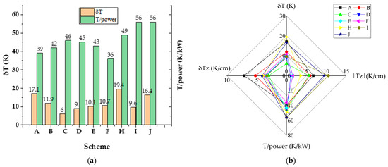
Figure 12.
Temperature difference and temperature per kW for different schemes. (a) Bar chart. (b) Radar chart.
4. Conclusions
The thermal field of 204 mm diameter SiC single crystal growth using the resistance method is simulated. Based on Ohm’s law, the current and potential of the heater were calculated, considering heat conduction, radiation, convective heat transfer, and non-isothermal flow inside the chamber. The temperature distribution and flow field distribution of the basic thermal field structure were obtained, and the main parameters such as temperature were basically consistent with the previous literature. Under the basic thermal field conditions, the growth interface temperature reaches above 2390 K, the radial temperature difference is relatively large, reaching about 15 K, the axial temperature gradient is about 6 K/cm, and the edge parameter is greater than the center parameter, which is not conducive to improving the crystal growth rate and suppressing edge polycrystals. Through structural adjustment, it has been shown that extending the length of the side heater and strengthening the insulation of the top edge area can help increase the edge temperature of the crystal growth interface and reduce the radial temperature difference. However, there is still the problem of an excessive edge temperature gradient, with the temperature gradient between the center and edge reaching twice the difference. Under the condition of extending the length of the heater, the radial temperature difference can be adjusted through increasing the thickness of the insulation, significantly reducing the value. However, the size of the axial temperature gradient significantly decreases to around 2 K/cm when the thickness reaches 24 mm. At the same time, the enhancement of the top insulation results in a minimum temperature gradient near the edge of the growth interface. Under the condition of using dual heaters and optimizing the insulation structure, a temperature gradient of about −10 K/cm was achieved, and the absolute value of the temperature gradient at the edge of the growth interface was smaller than that in the central region. Through increasing the axial temperature gradient, a small radial temperature difference was maintained, which is conducive to the suppression of edge polycrystals and the maintenance of the crystal growth rate. At the same time, this scheme has a high-energy consumption–temperature ratio. This study provides a useful reference for the growth of large-sized SiC crystals using the resistance method.
Supplementary Materials
The following supporting information can be downloaded at: https://www.mdpi.com/article/10.3390/cryst13121638/s1, Figure S1: Heat capacity of Argon; Figure S2: Density of Argon; Figure S3: Thermal conductivity of Argon; Figure S4: Thermal conductivity of SiC powder.
Author Contributions
Conceptualization, S.Z.; methodology, S.Z. and Z.L.; software, Z.L. and S.Z.; validation, T.L.; formal analysis, T.L. and S.Z.; investigation, T.L.; resources, L.Z.; data curation, S.Z.; writing—original draft preparation, S.Z.; writing—review and editing, J.S. and L.Z.; visualization, S.Z. and Z.L.; supervision, J.S., G.C. and L.Z.; project administration, T.L.; funding acquisition, L.Z. All authors have read and agreed to the published version of the manuscript.
Funding
This research was funded by Major Scientific and Technological Achievements Transformation Projects of Heilongjiang Province of China, grant number [CG20A008]; Natural Science Foundation of Heilongjiang Province, grant number [JJ2023JQ0025]; and Harbin Science and Technology Innovation Talents, grant number [2022HBRCGX014].
Institutional Review Board Statement
Not applicable.
Informed Consent Statement
Not applicable.
Data Availability Statement
The data presented in this study are available on request from the corresponding author.
Conflicts of Interest
Tie Li and Zhongxue Li are employee of Harbin KY Semiconductor, Inc.; Lili Zhao is an employee of Soft-Impact China (Harbin), Ltd. and Harbin KY Semiconductor, Inc. The remaining authors declare that the research was conducted in the absence of any commercial or financial relationships that could be construed as a potential conflict of interest.
References
- Powell, A.R.; Sumakeris, J.J.; Khlebnikov, Y.; Paisley, M.J.; Leonard, R.; Deyneka, E.; Gangwal, S.; Ambati, J.; Tsevtkov, V.; Seaman, J.; et al. Bulk Growth of Large Area SiC Crystals. Mater. Sci. Forum 2016, 858, 5–10. [Google Scholar] [CrossRef]
- Dhanaraj, G.; Huang, X.R.; Dudley, M.; Prasad, V.; Ma, R.H. Silicon Carbide Crystals—Part I: Growth and Characterization. In Crystal Growth Technology; William Andrew: Norwich, NY, USA, 2003; pp. 181–232. [Google Scholar]
- Ha, M.; Jeong, S. A Review of the Simulation Studies on the Bulk Growth of Silicon Carbide Single Crystals. J. Korean Ceram. Soc. 2022, 59, 153–179. [Google Scholar] [CrossRef]
- Wei, J.; Li, K.; Li, H.; Hou, D.; Zhang, Y.; Wang, C. Large-Scale Synthesis and Photoluminescence Properties of Hexagonal-Shaped SiC Nanowires. J. Alloys Compd. 2008, 462, 271–274. [Google Scholar] [CrossRef]
- Lebedev, A.A. Deep Level Centers in Silicon Carbide: A Review. Semiconductors 1999, 33, 107–130. [Google Scholar] [CrossRef]
- Tawada, Y.; Tsuge, K.; Kondo, M. Properties and Structure of a-SiC:H for High-Efficiency a-Si Solar Cell. J. Appl. Phys. 1982, 53, 5273–5281. [Google Scholar] [CrossRef]
- Wang, Y.; Gu, P.; Lei, P.; Wang, P.; Fu, J.; Yuan, L. Control of the Growth Quality by Optimizing the Crucible Structure for Growth of Large-Sized SiC Single Crystal. J. Cryst. Growth 2022, 600, 126929. [Google Scholar] [CrossRef]
- Kato, T.; Miura, T.; Nagai, I.; Taniguchi, H.; Kawashima, H.; Ozawa, T.; Arai, K.; Okumura, H. Enlargement Growth of Large 4H-SiC Bulk Single Crystal. Mater. Sci. Forum 2011, 679–680, 3–7. [Google Scholar] [CrossRef]
- Quast, J.; Hansen, D.; Loboda, M.; Manning, I.; Moeggenborg, K.; Mueller, S.; Parfeniuk, C.; Sanchez, E.; Whiteley, C. High Quality 150 mm 4H SiC Wafers for Power Device Production. Mater. Sci. Forum 2015, 821–823, 56–59. [Google Scholar] [CrossRef]
- Choi, J.W.; Kim, J.G.; Jang, B.K.; Ko, S.K.; Kyun, M.O.; Seo, J.D.; Ku, K.R.; Choi, J.M.; Lee, W.J. Modified Hot-Zone Design for Large Diameter 4H-SiC Single Crystal Growth. Mater. Sci. Forum 2019, 963, 18–21. [Google Scholar] [CrossRef]
- Ramakers, S.; Marusczyk, A.; Amsler, M.; Eckl, T.; Mrovec, M.; Hammerschmidt, T.; Drautz, R. Effects of Thermal, Elastic, and Surface Properties On the Stability of SiC Polytypes. Phys. Rev. B 2022, 106, 075201. [Google Scholar] [CrossRef]
- Guo, N.; Pei, Y.; Yuan, W.; Li, Y.; Zhao, S.; Yang, S.; Zhang, Y.; Liu, X. Layered Epitaxial Growth of 3C/4H Silicon Carbide Confined by Surface Micro-Nano Steps. Crystals 2023, 13, 1123. [Google Scholar] [CrossRef]
- Ellefsen, O.M.; Arzig, M.; Steiner, J.; Wellmann, P.; Runde, P. Optimization of the SiC Powder Source Material for Improved Process Conditions during PVT Growth of SiC Boules. Materials 2019, 12, 3272. [Google Scholar] [CrossRef] [PubMed]
- Liu, C.; Chen, X.; Peng, T.; Wang, B.; Wang, W.; Wang, G. Step Flow and Polytype Transformation in Growth of 4H-SiC Crystals. J. Cryst. Growth 2014, 394, 126–131. [Google Scholar] [CrossRef]
- Fan, W.; Qu, H.; Chang, S.I.; Kozak, B.; Shaffer, G.; Galyukov, A.; Lee, W.J. Impacts of Tac Coating On SiC PVT Process Control and Crystal Quality. Mater. Sci. Forum 2019, 963, 22–25. [Google Scholar] [CrossRef]
- Chen, Q.; Zhu, P.; He, M. Simulations of Dislocation Density in Silicon Carbide Crystals Grown by the PVT-Method. J. Cryst. Growth 2020, 531, 125380. [Google Scholar] [CrossRef]
- Steiner, J.; Wellmann, P.J. Impact of Mechanical Stress and Nitrogen Doping on the Defect Distribution in the Initial Stage of the 4H-SiC PVT Growth Process. Materials 2022, 15, 1897. [Google Scholar] [CrossRef]
- Wang, H.; Yu, J.; Hu, G.; Peng, Y.; Xie, X.; Hu, X.; Chen, X.; Xu, X. Micropipes in SiC Single Crystal Observed by Molten KOH Etching. Materials 2021, 14, 5890. [Google Scholar] [CrossRef]
- Liang, L.; Li, S.; Chai, P.; Lan, K.; Yu, R. Molecular Dynamics Simulation of Single-Crystal 4H-SiC Nano Scratching with Different Scratching Directions of the Tool. Crystals 2023, 13, 1044. [Google Scholar] [CrossRef]
- Hayashi, Y.; Mitani, T.; Komatsu, N.; Kato, T.; Okumura, H. Control of Temperature Distribution to Suppress Macro-Defects in Solution Growth of 4H-SiC Crystals. J. Cryst. Growth 2019, 523, 125151. [Google Scholar] [CrossRef]
- Yang, N.; Song, B.; Wang, W.; Li, H. Control of the Temperature Field by Double Induction Coils for Growth of Large-Sized SiC Single Crystals via the Physical Vapor Transport Technique. CrystEngComm 2022, 24, 3475–3480. [Google Scholar] [CrossRef]
- Kawanishi, S.; Shibata, H.; Yoshikawa, T. Contribution of Dislocations in SiC Seed Crystals on the Melt-Back Process in SiC Solution Growth. Materials 2022, 15, 1796. [Google Scholar] [CrossRef]
- Zhang, S.; Fan, G.; Li, T.; Zhao, L. Optimization of Thermal Field of 150 mm SiC Crystal Growth by PVT Method. RSC Adv. 2022, 12, 19936–19945. [Google Scholar] [CrossRef]
- Gao, P.; Xin, J.; Liu, X.; Zheng, Y.; Shi, E. Control of 4H Polytype of SiC Crystals by Moving up the Crucible to Adjust the Temperature Field of the Growth Interface. CrystEngComm 2019, 21, 6964–6968. [Google Scholar] [CrossRef]
- Yang, C.; Liu, G.; Chen, C.; Hou, Y.; Xu, M.; Zhang, Y. Numerical Simulation of Temperature Fields in a Three-Dimensional SiC Crystal Growth Furnace with Axisymmetric and Spiral Coils. Appl. Sci. 2018, 8, 705. [Google Scholar] [CrossRef]
- Luo, H.; Han, X.; Huang, Y.; Yang, D.; Pi, X. Numerical Simulation of a Novel Method for PVT Growth of SiC by Adding a Graphite Block. Crystals 2021, 11, 1581. [Google Scholar] [CrossRef]
- Goldberg, Y.; Levinshtein, M.E.; Rumyantsev, S.L. Properties of Advanced Semiconductor Materials: GaN, AIN, InN, BN, SiC, SiGe; John Wiley: Hoboken, NJ, USA, 2001. [Google Scholar]
- Shaffer, P.T.B. A Review of the Structure of Silicon Carbide. Acta Crystallogr. 2010, B25, 477–488. [Google Scholar] [CrossRef]


Disclaimer/Publisher’s Note: The statements, opinions and data contained in all publications are solely those of the individual author(s) and contributor(s) and not of MDPI and/or the editor(s). MDPI and/or the editor(s) disclaim responsibility for any injury to people or property resulting from any ideas, methods, instructions or products referred to in the content. |
© 2023 by the authors. Licensee MDPI, Basel, Switzerland. This article is an open access article distributed under the terms and conditions of the Creative Commons Attribution (CC BY) license (https://creativecommons.org/licenses/by/4.0/).