Abstract
Spontaneous Sn whisker growth, as a reliability issue in electronic assemblies, has drawn much attention in the past several decades. However, the underlying mechanism is still ambiguous. Herein, the growth of Sn whiskers on pure Sn with different specific surface areas was studied to elucidate the effect of surface energy on Sn whisker growth. Though fabricated and cultivated using the same parameters, it was found that Sn whiskers were obtained on the sample of nano-Sn, which possesses excess surface energy, while no whiskers were observed on the sample of micro-Sn, indicating that surface energy plays a significant role in Sn whisker growth. In addition, the whiskering phenomenon is confirmed to be an abnormal recrystallization process according to the microstructure of the whisker root. Therefore, a Sn whisker growth mechanism companied with an abnormal recrystallization process is proposed, which is driven by the excess surface energy. This work provides a new perspective on understanding the long-standing Sn whiskering problem.
1. Introduction
Spontaneous Sn whisker growth has been a considerable reliability risk for more than 70 years, as it can cause electrical failures and even tremendous disasters in electronics-rich systems [1,2,3,4]. The development of lead-free movement made this problem even more serious, since the generally accepted whisker mitigation strategy, to alloy Sn with lead, was to be phased out. Understanding the mechanism behind Sn whisker growth is therefore of prime importance. In fact, a number of Sn whisker growth mechanisms have been proposed to date, including the dislocation mechanism [5,6], recrystallization mechanism [7], active Sn atom mechanism [8], electrostatic mechanism [9], etc. Among these, the compressive stress mechanism [10,11,12,13] is most widely accepted. However, there are still many phenomena that cannot be properly explained by the compressive stress mechanism.
The volume expansion associated with the formation of Cu6Sn5 at the interface between Sn and the underlying Cu substrate has been widely considered to be the origin of stress in Sn platings. However, the growth of metal whiskers in Al–Sn [14] and Si–Sn [15] systems have also been reported, in which intermetallic compounds (IMCs) are lacking. The thermal expansion mismatch and oxidation of whiskering metal were proposed to be the origin of stress in the above cases. However, by characterizing Sn whisker growth behavior in systems with different thermal expansion mismatch, it was found that the Sn whisker growth tendency is not thermal-expansion-mismatch-dependent [16,17], suggesting that the stress induced by thermal expansion mismatch is probably not the fundamental driving force. Meanwhile, whiskers were still observed on the sample cultivated at high vacuum conditions [18], and even grew faster in a vacuum than in air in specific conditions [19]. In addition, the reversible whiskering phenomenon, which indicates that the whisker growth was driven by a reversible force, was reported [20,21]. Considering that the driving force from stress in irreversible, it is reasonable to assume that compressive stress is not a necessary factor for whisker growth.
It is interesting that more and more metal whiskering phenomena on high surface/interface energy systems have been found in recent years. For example, Bi whisker growth in non-wetting Bi–V systems, which was mainly attributed to the excessive surface energy of Bi, was reported by Liu et al. [22]. Similarly, Kosinova et al. [23] reported the growth of Au whiskers in glass–Au–Al2O3 systems, in which the main driving force was proposed to be the reduction in interface energy. Furthermore, it has been well established that bright Sn plating with fine grains more easily grows Sn whiskers than the matte one, and the whisker growth tendency is inversely proportional to the plating thickness [24,25]. These results suggest that surface/interface energy may play a significant role in whisker growth. However, the specific effect of surface/interface energy on Sn whisker growth has been seldom reported until now, which is probably related to the difficulty in decoupling the numerous factors affecting Sn whisker growth.
In the present work, we developed a simple pure Sn system, in which the specific surface area is adjusted by choosing Sn powders with different particle sizes to study the whisker growth behavior, thereby revealing the underlying mechanisms. The Sn whisker growth behavior on the samples is observed to make clear the effect of surface energy on whisker growth. Afterwards, an in situ observation of Sn whisker growth, together with cross-sectional observation of the microstructure at the whisker root, are conducted to understand the whisker growth process. Finally, a surface energy mechanism, in which the whisker growth through an abnormal recrystallization process driven by the excess surface energy, is proposed.
2. Experimental Procedure
Both nano-Sn powder (99.9%) and micro-Sn powder (99.5%) were cold-pressed under 200 MPa into discs of 15 mm diameter and 2~3 mm thickness. Then, the green discs were cultivated at room temperature and observed periodically to record the whisker growth behavior.
The chemical composition of both nano-Sn powder and micro-Sn powder has been detected using inductively coupled plasma optical emission spectroscopy (ICP-OES, iCAP PRO, Thermo Fisher, Waltham, MA, USA), and the results are listed in Table 1. The morphologies of the substrate and the Sn whisker were examined using a scanning electron microscope (SEM, Sirion 200, FEI, Hillsboro, OR, USA) and transmission electron microscopy (TEM, Tecnai G2-T20, FEI, Hillsboro, OR, USA). In addition, the cross-sectional microstructure of the whisker root was obtained using dual beam microscopy (SEM-FIB, 3D, FEI, Hillsboro, OR, USA). The residual stress of the cold-pressed discs was measured using X-ray diffraction (XRD, D8 Discover, Bruker, Billerica, MA, USA) using the sin2φ technique [26]. The offset angle (φ) was 0°, 15°, 30°, and 45°. The 2θ diffraction peak of 103.41° corresponding to the (213) plane of β-Sn was used to calculate the residual stress. Both the nano-Sn and micro-Sn powder were studied with the aid of differential scanning calorimetry (DSC, STA 449F5, Netzsch, Selb, Germany) in a dry nitrogen atmosphere at heating rates of 10 °C/min.

Table 1.
Chemical composition of both nano-Sn powder and micro-Sn powder (wt.%).
3. Results and Discussion
3.1. Sn Whisker Growth on Pure Sn System
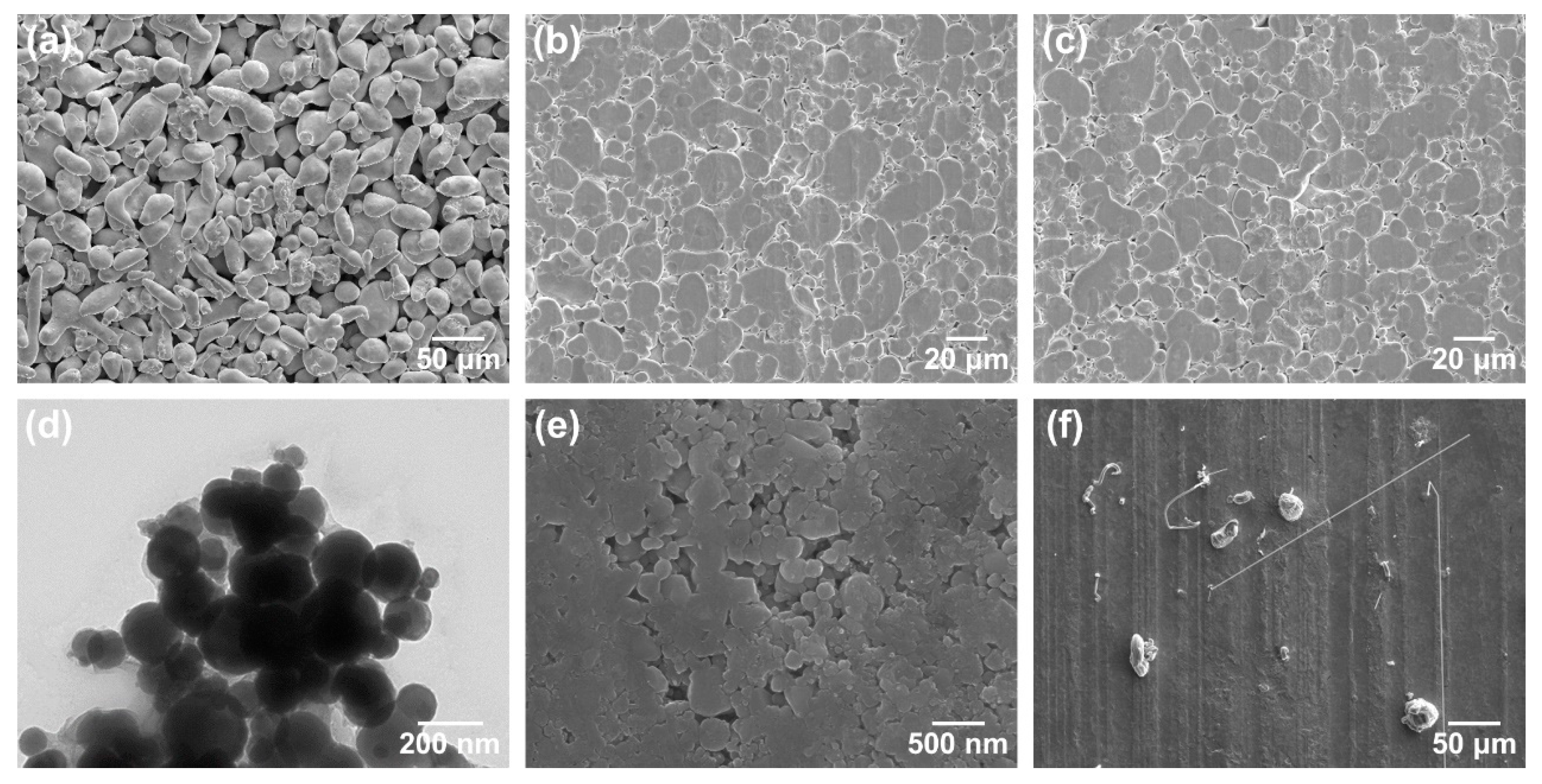
Figure 1a,d show a micrograph of the micro-Sn and nano-Sn powder used to prepare the pure Sn samples with different specific surface areas, respectively. It can be observed that the particle size of the pebble-like micro-Sn ranges from 10 to 80 μm, while the spherical nano-Sn ranges from 20 to 200 nm. Figure 1b,e show the surface morphology of the micro-Sn and nano-Sn sample, respectively. Sn whiskers were observed on the nano-Sn sample after only 1 day. And more whiskers grew from the sample with the further extension of cultivating time. However, no whiskers were observed on the micro-Sn sample, even after the extension of cultivating time to more than 1 year, as displayed in Figure 1c. Figure 1f shows the whisker growth behavior on the nano-Sn sample after cultivating at room temperature for 3 days. A few whiskers can be observed on the nano-Sn sample. In addition to the typically filamentary whiskers with an approximate diameter of 1 μm, a few thick whiskers with low aspect ratio can be also observed, which was generally observed when cultivated in high temperatures and a high humidity environment [25,27].

Figure 1.
Micrograph of (a) micro-Sn powder; (b) as-prepared micro-Sn sample; (c) Sn whisker growth behavior on nano-Sn sample after cultivating in room ambience for 1 year; (d) nano-Sn powder; (e) as-prepared nano-Sn sample; (f) Sn whisker growth behavior on nano-Sn sample after cultivating in room ambience for 3 days.
A magnified view of the Sn whiskers grown on the nano-Sn sample is displayed in Figure 2. A smooth surface with striations along the growth direction was observed on the filamentary whiskers, as shown in Figure 2a, which is similar to the whiskers formed on Sn platings and solders. Figure 2b shows a thick whisker with an approximate diameter of approximately 10 μm, and the size remained unchanged during the whiskering process. Meanwhile, thick whiskers with variable cross-sections were also observed, as typically displayed in Figure 2c. And a cap that shares the same features as the sample surface can be observed on the top of the whisker, as indicated by the white arrow in Figure 2c, suggesting that the whiskers probably nucleate from the surface Sn. In addition, a single crystalline feature was observed at the whisker root area, as shown in Figure 2d. According to the micrograph, the diameter of the grains is approximately 10 μm. Given that the diameter of the nano-Sn particle is smaller than 200 nm, the formation of these large grains should be related to the recrystallization process.
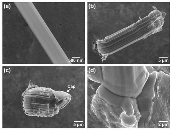
Figure 2.
Characteristics of the whiskers grown on the nano-Sn sample: (a) filamentary whisker; (b) thick whisker with constant cross-section; (c) thick whisker with variable cross-section; (d) recrystallization trace at whisker root area.
3.2. In Situ Observation of Sn Whisker Growth
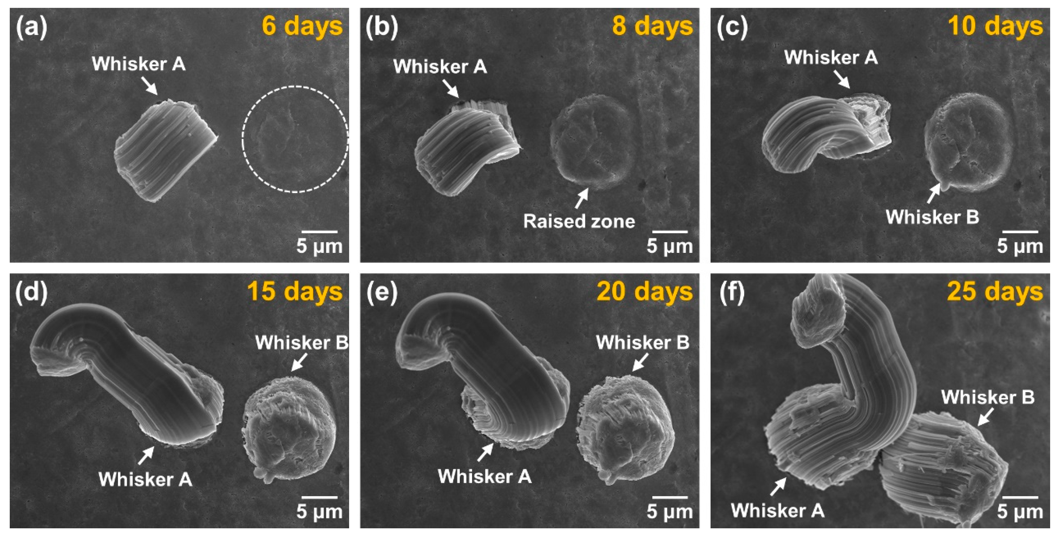
To elucidate the whisker growth process, several zones on the whiskering sample were observed in situ, as presented in Figure 3. After being cultivated at room temperature for 6 days, a thick whisker could be observed on the nano-Sn sample surface, labeled as whisker A in Figure 3a. With the extension of the cultivation period up to 8 days, a hump, as shown in Figure 3b, located in the white circled area in Figure 3a, formed on the side of the whisker A. As the cultivation time was prolonged, the hump developed into a thick whisker (labeled as whisker B), and whisker A also grew longer. According to the whisker growth process, it can be confirmed that Sn whiskers nucleate from a block of Sn on the surface. In addition, once the whisker grew out of the substrate, the geometrical morphology remained unchanged, suggesting that Sn whisker growth proceeds by adding atoms to the base. It can also be deduced that the variable cross-section associated with Sn whisker growth is the result of the whisker root size changing, rather than the result of morphological evolution after the whisker formed.
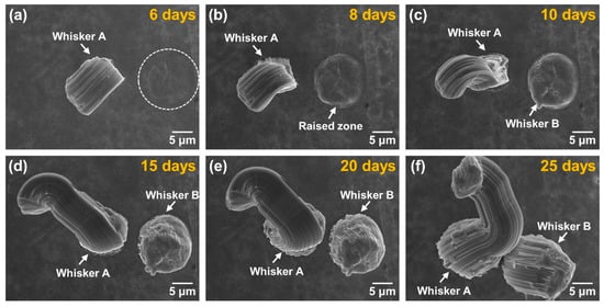
Figure 3.
Sn whisker growth behavior of the nano-Sn sample after cultivating at room temperature for (a) 6 days; (b) 8 days; (c) 10 days; (d) 15 days; (e) 20 days; (f) 25 days.
3.3. Microstructure at the Root of Sn Whiskers
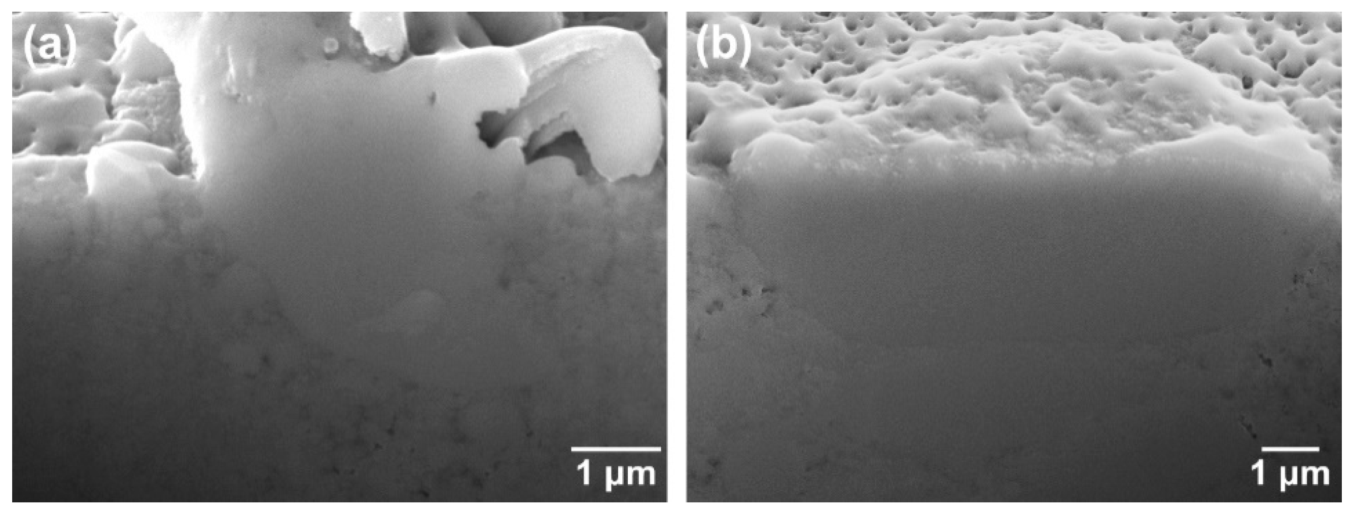
For a precise understanding of whether Sn whisker growth is the result of recrystallization, FIB cross-sectioning at the base of the whiskers was performed. Figure 4a shows the cross-sectional microstructure of a Sn whisker that has grown out of the substrate. A clear interface can be observed between the whisker root and the substrate. The whisker root embedded in the substrate is a big grain, while the substrate around the root was composed of numerous grains of a much smaller size. Meanwhile, the cross-sectional morphology of a whisker just protruded from the surface shows the same feature, as displayed in Figure 4b. Due to the fact that the substrate was prepared using nano-Sn particles, the formation of the large whisker root must experience recrystallization. In addition, as can be seen in Figure 1f, Sn whiskers only grow on a small fraction of the sample. Therefore, it is reasonable to deduce that the Sn whisker growth on the nano-Sn sample is an abnormal recrystallization process.

Figure 4.
Cross-sectional microstructure at the root of Sn whiskers: (a) a whisker has grown out of the substrate; (b) a whisker just protruded from the substrate.
3.4. Surface-Energy-Driven Sn Whisker Growth
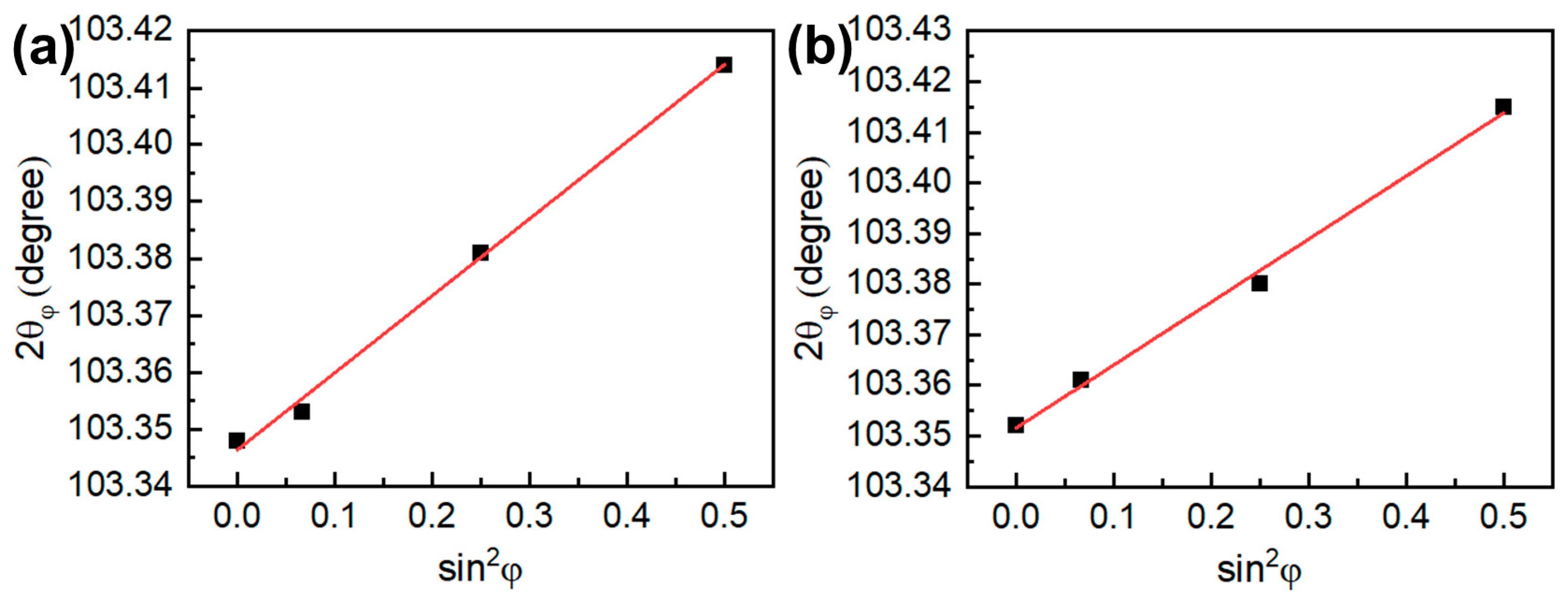
In the present work, both the micro-Sn and nano-Sn sample were prepared via cold-pressing. To evaluate the effect of residual stress on Sn whisker growth, the stress in the cold-pressed samples was measured using XRD, which can be obtained using the following equation:
where E and υ are the elastic modulus and Poisson’s ratio of Sn, the Bragg’s angle 2θ0 is considered a constant of 103.41°, 2θ is the diffraction angle with residual stress, and φ is the offset angle of the X-ray. The elastic modulus and Poisson’s ratio of Sn are 50 GPa and 0.36, respectively [28].
According to the result of 2θ vs. sin2φ displayed in Figure 5, the residual stress in the micro-Sn sample is calculated as 34.3 ± 1.4 MPa, and in the nano-Sn one it is calculated as 31.5 ± 1.5 MPa. The slight residual stress difference suggests that residual stress is not the major driving force for whisker growth in this system, although it is difficult to exclude the effect of compressive stress on whisker growth.
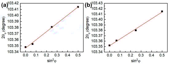
Figure 5.
The result of 2θ versus sin2φ. (a) micro-Sn sample; (b) nano-Sn sample.
In general, cold deformation could promote recrystallization. However, Sn whiskers were only observed on the nano-Sn sample, which suggests that another factor provides the main driving force for Sn whisker growth. Herein, the major difference between the micro-Sn and nano-Sn sample is the particle size of the raw materials, which can directly affect the specific surface area. For a given particle, the relationship between the specific surface area and melting point can be described using the following equation:
where S is the surface area divided by volume, η is related to the surface energy of the solid and liquid phases, Tm is the melting point of the particle, and T0 is the melting point of the corresponding bulk. Given that η and T0 are constant for a certain matter, it is obvious that a larger S indicates a lower Tm.
Afterwards, both the micro-Sn and nano-Sn powder were studied using DSC to detect the melting point. As shown in Figure 6, the melting point of micro-Sn powder was determined to be 232.1 °C, which is in good accordance with the result of bulk Sn. Meanwhile, the melting point of nano-Sn powder was measured to be 227.4 °C, approximately 5 °C lower than bulk Sn. Accordingly, it can be concluded that the specific surface area of nano-Sn powder is larger than the micro-Sn powder. Considering that specific surface area is the major difference between the micro-Sn and nano-Sn sample, it is reasonable to assume that the excess surface energy provides the main driving force for the whiskering phenomenon. It is worthwhile pointing out that the impurities in the substrate may also affect the surface energy of materials.
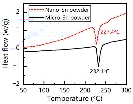
Figure 6.
DSC curves of micro-Sn and nano-Sn powder.
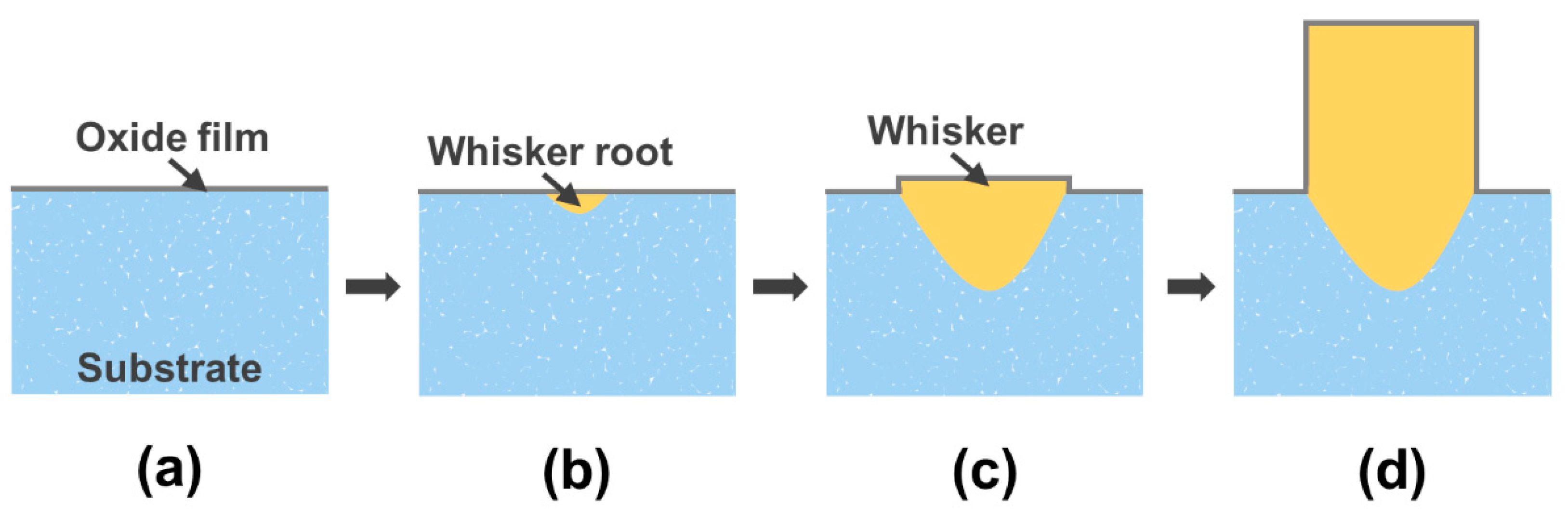
Based on the previous results and analysis, a surface-energy-driven mechanism for Sn whisker growth is proposed and schematically illustrated in Figure 7. The substrate pressed using nano-Sn powder, as shown in Figure 7a, has an excess surface energy larger than that of bulk Sn. It is worthwhile pointing out that a layer of oxide film will be formed on the surface when the sample is exposed to air. Precisely because of the existence of the oxide film, the top of the Sn whisker maintains the same morphological features as the sample surface rather than appearing as faceted morphology. Driven by the excess surface energy, some grains start to grow through abnormal recrystallization, as shown in Figure 7b. In this stage, no changes can be observed on the surface of the substrate. Once the grain boundary is pinned by defects or impurities, it will penetrate the oxidized surface and thus appear as a whisker, as shown in Figure 7c. With the continuous feeding of Sn atoms to the whisker root, the whisker grows longer over time, as shown in Figure 7d. If the pinning is variable during whisker growth, the cross-section of the whisker becomes larger, resulting into the formation of a whisker with a variable diameter, as displayed in Figure 2c.
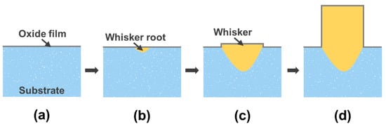
Figure 7.
Schematic of the surface-energy-driven Sn whisker growth process. (a) As-prepared nano-Sn substrate with excess surface energy; (b) Sn whisker root formed by abnormal recrystallization driven by the excess surface energy; (c) Sn whisker that has just penetrated the oxidized surface; (d) Sn whisker growth by continuous Sn atoms adding to the root.
4. Conclusions
In this work, the Sn whisker growth behavior on Sn with different surface energy was studied. It was found that Sn whiskers grow easily on nano-Sn with higher surface energy, while no whiskers were observed on micro-Sn. In addition, Sn whisker root formation by abnormal recrystallization was observed, and the storage of excess surface energy on nano-Sn was confirmed. Based on the experimental results, a Sn whisker growth mechanism is proposed, in which Sn whiskers grow through abnormal recrystallization driven by the excess surface energy. It is worth noting that this mechanism does not deny the effect of other factors on Sn whisker growth, but makes clear that surface/interface energy does play a significant role on the growth of Sn whiskers. The findings shed new light on our understanding of the whiskering phenomenon, which has resisted interpretation for around 70 years.
Author Contributions
Conceptualization, Y.L. (Yushuang Liu), M.H. and Y.C.; methodology, Y.L. (Yushuang Liu), Y.L. (Ying Liu) and Y.Z.; software, M.H. and L.C.; validation, Y.L. (Yushuang Liu) and L.C.; formal analysis, Y.L. (Yushuang Liu), M.H. and Y.C.; investigation, Y.L. (Yushuang Liu), M.H. and Y.C.; resources, Y.C.; data curation, Y.L. (Ying Liu) and Y.Z.; writing—original draft preparation, Y.L. (Yushuang Liu) and M.H.; writing—review and editing, Y.L. (Yushuang Liu); visualization, Y.C.; supervision, Y.L. (Yushuang Liu); project administration, Y.L. (Yushuang Liu); funding acquisition, Y.L. (Yushuang Liu). All authors have read and agreed to the published version of the manuscript.
Funding
The research was supported by the National Natural Science Foundation of China, grant number 52001158, and the Scientific Research Foundation of Nanjing Institute of Technology, grant number YKJ202005.
Data Availability Statement
Data is contained within the article.
Conflicts of Interest
The authors declare no conflict of interest.
References
- Compton, K.G.; Mendizza, A.; Arnold, S.M. Filamentary growth on metal surfaces—“Whiskers”. Corrosion 1951, 7, 327–334. [Google Scholar] [CrossRef]
- Galyon, G.T. Annotated tin whisker bibliography and anthology. IEEE Trans. Electron. Packag. Manuf. 2005, 28, 94–122. [Google Scholar] [CrossRef]
- Osenbach, J.W.; DeLucca, J.M.; Potteiger, B.D.; Amin, A.; Baiocchi, F.A. Sn-whiskers: Truths and myths. J. Mater. Sci. Mater. Electron. 2007, 18, 283–305. [Google Scholar] [CrossRef]
- NASA. Available online: http://nepp.nasa.gov/whisker/failures/index.htm (accessed on 30 October 2023).
- Eshelby, J.D. A tentative theory of metallic whisker growth. Phys. Rev. Lett. 1953, 91, 755–756. [Google Scholar]
- Frank, F.C. XC. On tin whiskers. Philos. Mag. 1953, 44, 854–860. [Google Scholar] [CrossRef]
- Ellis, W.C.; Gibbons, D.F.; Treuning, R.C. Growth of Metal Whiskers from the Solid, Growth and Perfection of Crystals; John Wiley & Sons: New York, NY, USA, 1958; pp. 102–120. [Google Scholar]
- Xian, A.P.; Liu, M. Observations of continuous tin whisker growth in NdSn3 intermetallic compound. J. Mater. Res. 2009, 24, 2775–2783. [Google Scholar] [CrossRef]
- Subedi, B.; Niraula, D.; Karpov, V.G. The stochastic growth of metal whiskers. Appl. Phys. Lett. 2017, 110, 251604. [Google Scholar] [CrossRef]
- Tu, K.N. Irreversible processes of spontaneous whisker growth in bimetallic Cu-Sn thin-film reactions. Phys. Rev. B 1994, 49, 2030–2034. [Google Scholar] [CrossRef]
- Tu, K.N.; Li, J.C.M. Spontaneous whisker growth on lead-free solder finishes. Mat. Sci. Eng. A 2005, 409, 131–139. [Google Scholar] [CrossRef]
- Dudek, M.; Chawla, N. Mechanisms for Sn whisker growth in rare earth-containing Pb-free solders. Acta Mater. 2009, 57, 4588–4599. [Google Scholar] [CrossRef]
- Pei, F.; Buchovecky, E.; Bower, A.; Chason, E. Stress evolution and whisker growth during thermal cycling of Sn films: A comparison of analytical modeling and experiments. Acta Mater. 2017, 129, 462–473. [Google Scholar] [CrossRef]
- Zhang, Y.; Zhang, P.; He, W.; Sun, Z.M. Tin whisker growth on immiscible Al–Sn alloy. J. Mater. Sci. Mater. Electron. 2020, 31, 1328–1334. [Google Scholar] [CrossRef]
- Xiao, X.; Sachdev, A.K.; Haddad, D.; Li, Y.; Sheldon, B.W.; Soni, S.K. Stress-induced Sn nanowires from Si-Sn nanocomposite coatings. Appl. Phys. Lett. 2010, 97, 141904. [Google Scholar] [CrossRef]
- Crandall, E.R.; Flowers, G.T.; Dean, R.N.; Bozack, M.J. Growth of Sn Whiskers on Semiconductor and Insulator Surfaces. In Proceedings of the 56th IEEE Holm Conference on Electrical Contacts, Charleston, SC, USA, 4–7 October 2010. [Google Scholar]
- Bozack, M.J.; Snipes, S.K.; Flowers, G.N. Methods for fast, reliable growth of Sn whiskers. Surf. Sci. 2016, 652, 355–366. [Google Scholar] [CrossRef]
- Barsoum, M.W.; Hoffman, E.N.; Doherty, R.D.; Gupta, S.; Zavaliangos, A. Driving force and mechanism for spontaneous metal whisker formation. Phys. Rev. Lett. 2004, 93, 206104. [Google Scholar] [CrossRef] [PubMed]
- Suganuma, K.; Baated, A.; Kim, K.S.; Hamasaki, K.; Nemoto, N.; Nakagawa, T.; Yamada, T. Sn whisker growth during thermal cycling. Acta Mater. 2011, 59, 7255–7267. [Google Scholar] [CrossRef]
- Sun, Z.M.; Barsoum, M.W. Alternate mechanism for the spontaneous formation of freestanding Ga nanoribbons on Cr2GaC surfaces. J. Mater. Res. 2006, 21, 1629–1631. [Google Scholar] [CrossRef]
- Sun, Z.M.; Barsoum, M.W.; Zhang, Y.M.; Hashimoto, H. On Equilibrium Ga Intergranular Films in Cr2GaC. Mater. Res. Lett. 2013, 1, 109–113. [Google Scholar] [CrossRef]
- Liu, M.; Tao, J.; Nam, C.Y.; Kisslinger, K.; Zhang, L.; Su, D. Surface-Energy Induced Formation of Single Crystalline Bismuth Nanowires over Vanadium Thin Film at Room Temperature. Nano Lett. 2014, 14, 5630–5635. [Google Scholar] [CrossRef] [PubMed]
- Kosinova, A.; Wang, D.; Schaaf, P.; Sharma, A.; Klinger, L.; Rabkin, E. Whiskers growth in thin passivated Au films. Acta Mater. 2018, 149, 154–163. [Google Scholar] [CrossRef]
- Lee, B.Z.; Lee, D.N. Spontaneous growth mechanism of tin whiskers. Acta Mater. 1998, 46, 3701–3714. [Google Scholar] [CrossRef]
- Vianco, P.T.; Neilsen, M.K.; Rejent, J.A.; Grant, R.P. Validation of the Dynamic Recrystallization (DRX) Mechanism for Whisker and Hillock Growth on Sn Thin Films. J. Electron. Mater. 2015, 44, 4012–4034. [Google Scholar] [CrossRef]
- Baated, A.; Kim, K.S.; Suganuma, S. Whisker growth from an electroplated zinc coating. J. Mater. Res. 2010, 25, 2175–2182. [Google Scholar] [CrossRef]
- Li, C.F.; Liu, Z.Q.; Shang, J.K. The effects of temperature and humidity on the growth of tin whisker and hillock from Sn5Nd alloy. J. Alloys Compd. 2013, 550, 231–238. [Google Scholar] [CrossRef]
- Tian, S.; Cao, R.; Zhou, J.; Xue, F.; Liu, Y.; Zhang, P.; Sun, Z.M. A comparative study on the growth behaviors of Sn whiskers and hillocks in a Sn-Al alloy coating under different environments. J. Alloys Compd. 2021, 853, 157101. [Google Scholar] [CrossRef]


Disclaimer/Publisher’s Note: The statements, opinions and data contained in all publications are solely those of the individual author(s) and contributor(s) and not of MDPI and/or the editor(s). MDPI and/or the editor(s) disclaim responsibility for any injury to people or property resulting from any ideas, methods, instructions or products referred to in the content. |
© 2023 by the authors. Licensee MDPI, Basel, Switzerland. This article is an open access article distributed under the terms and conditions of the Creative Commons Attribution (CC BY) license (https://creativecommons.org/licenses/by/4.0/).