Article

NiO/Ga2O3 Vertical Rectifiers of 7 kV and 1 mm2 with 5.5 A Forward Conduction Current

1
Department of Chemical Engineering, University of Florida, Gainesville, FL 32611, USA
2
Department of Material Science and Engineering, University of Florida, Gainesville, FL 32611, USA
*
Author to whom correspondence should be addressed.
Crystals 2023, 13(12), 1624; https://doi.org/10.3390/cryst13121624
Submission received: 21 October 2023 / Revised: 20 November 2023 / Accepted: 21 November 2023 / Published: 23 November 2023
(This article belongs to the Special Issue Wide-Bandgap Semiconductor Materials, Devices and Systems)

Abstract

:
In this study, we present the fabrication and characterization of vertically oriented NiO/β polymorph n-Ga2O3/n+ Ga2O3 heterojunction rectifiers featuring a substantial area of 1 mm2. A dual-layer SiNX/SiO2 dielectric field plate edge termination was employed to increase the breakdown voltage (VB). These heterojunction rectifiers exhibit remarkable simultaneous achievement of high breakdown voltage and substantial conducting currents. In particular, the devices manifest VB of 7 kV when employing a 15 µm thick drift layer doping concentration of 8.8 × 1015 cm−3, concurrently demonstrating a forward current of 5.5 A. The thick drift layer is crucial in obtaining high VB since similar devices fabricated on 10 µm thick epilayers had breakdown voltages in the range of 3.6–4.0 kV. Reference devices fabricated on the 15 µm drift layers had VB of 5 kV. The breakdown is still due to leakage current from tunneling and thermionic emission and not from avalanche breakdown. An evaluation of the power figure-of-merit, represented by VB2/RON, reveals a value of 9.2 GW·cm−2, where RON denotes the on-state resistance, measuring 5.4 mΩ·cm2. The Coff was 4 nF/cm2, leading to an RON × Coff of 34 ps and FCO of 29 GHz. The turn-on voltage for these rectifiers was ~2 V. This exceptional performance surpasses the theoretical unipolar one-dimensional (1D) limit of both SiC and GaN, underscoring the potential of β-Ga2O3 for forthcoming generations of high-power rectification devices.

1. Introduction

The contemporary focus of research in power electronics revolves around the advancement of devices reliant on monoclinic β-Ga2O3 [1,2,3,4,5,6,7,8,9,10,11,12,13,14,15,16]. Notable demonstrations have unveiled the attainment of elevated breakdown voltages, surpassing 8 kilovolts (kV), albeit in relatively small diameter (100 µm) devices encompassing both vertical rectifiers [9,17,18,19] and lateral transistors tailored for applications necessitating lower current capacities [7,8]. Typically, standard Schottky Barrier Diodes (SBDs) have soft breakdown characteristics because of the Schottky barrier lowering at high reverse bias that allows tunneling and thermionic emission currents. Consequently, the breakdown voltage is chiefly determined using the maximum permissible leakage current rather than avalanche breakdown, representing a key limitation in their operational constraints [20,21,22,23,24]. A promising recent development entails the incorporation of NiO as a p-type conducting layer to engender p-n heterojunctions with the n-type Ga2O3 [21,25,26,27,28,29,30,31,32,33,34,35,36,37,38,39,40,41,42,43,44,45,46,47,48,49,50,51,52], partially mitigating the inherent absence of native p-type doping capabilities in Ga2O3. Nevertheless, formidable challenges persist, encompassing the optimization of edge termination and effective heat dissipation management, vital prerequisites for ensuring device reliability [1,5,20,25,32,33,34,35,36,37,38]. Another paramount endeavor entails the realization of larger area devices capable of facilitating substantial conduction currents, while concurrently upholding their kV-level breakdown characteristics [1,22,25,29,30,31,33,35].
Ga2O3 has emerged as a promising material for power electronics due to its unique combination of wide bandgap, high breakdown voltage, and excellent thermal stability. This article provides a detailed review of the recent progress and advantages in Gallium oxide power electronics, covering various aspects such as diodes, rectifiers, manufacturability, thermal conductivity limitations, large-area devices for high conduction currents, polymorphs, and the outlook for ultrawide semiconductor power electronics. The demand for more efficient and compact power electronic devices has driven extensive research into alternative materials beyond conventional silicon. Gallium oxide, with its wide bandgap of around 4.8 eV, stands out as a promising candidate for power electronics applications. This article delves into the recent advancements and advantages of Gallium oxide power electronics, examining key aspects that contribute to its potential in various applications.
One of the primary applications of Gallium oxide in power electronics is in the development of high-performance diodes and rectifiers. The wide bandgap of Ga2O3 enables the fabrication of diodes with high breakdown voltages, making them suitable for high-power applications. Recent research has focused on optimizing the design and fabrication processes to enhance the efficiency and reliability of Ga2O3 diodes. The advantages of Ga2O3 diodes include low on-state voltage drop, low reverse recovery time, and excellent temperature stability. These characteristics make Gallium oxide diodes well suited for applications where fast switching and high-temperature operation are crucial, such as in power inverters and converters. Manufacturability is a critical aspect of any semiconductor material’s viability for commercial applications. Gallium oxide has shown promise in terms of manufacturability, with researchers exploring scalable and cost-effective fabrication techniques. The development of reliable deposition methods, such as metal-organic chemical vapor deposition (MOCVD) and molecular beam epitaxy (MBE), has facilitated the production of high-quality Ga2O3 thin films for device fabrication.
Furthermore, advancements in process optimization and automation have streamlined manufacturing processes, contributing to the commercial feasibility of Gallium oxide-based power electronic devices. The ongoing efforts in improving yield, reducing fabrication costs, and enhancing production scalability are pivotal for the widespread adoption of Ga2O3 in power electronics. While Gallium oxide exhibits excellent electrical properties, its thermal conductivity is a limiting factor for certain high-power applications. The intrinsic thermal conductivity of Ga2O3 is relatively low compared to other wide-bandgap materials, leading to challenges in managing heat dissipation in power electronic devices. Researchers are actively addressing this limitation via the development of innovative thermal management techniques and materials. The incorporation of advanced thermal interface materials and heat spreaders, coupled with optimized device packaging, aims to mitigate thermal challenges and enhance the overall performance and reliability of Gallium oxide power electronic devices. To meet the demands of high-power applications, the need for large-area devices capable of handling substantial conduction currents is essential. Gallium oxide’s intrinsic properties, including its wide bandgap and high breakdown voltage, position it favorably for the fabrication of large-area power electronic devices.
Recent progress in the design and fabrication of large-area Ga2O3 devices has demonstrated the feasibility of achieving high conduction currents while maintaining the material’s advantageous characteristics. These developments open up new possibilities for Gallium oxide in applications requiring robust and high-power capabilities, such as electric vehicles, renewable energy systems, and power grids. Gallium oxide exists in different polymorphic forms, each with distinct crystal structures and properties. The most common polymorphs are β-Ga2O3 and α-Ga2O3. β-Ga2O3, with its monoclinic crystal structure, is thermodynamically stable at higher temperatures, while α-Ga2O3, with a rhombohedral crystal structure, is stable at lower temperatures.
Understanding the polymorphic behavior of Gallium oxide is crucial for tailoring its properties to specific applications. Researchers are exploring the synthesis and manipulation of different polymorphs to achieve desired electrical and thermal characteristics, further expanding the versatility of Ga2O3 in power electronics. Looking ahead, the outlook for ultrawide semiconductor power electronics, with Gallium oxide playing a central role, appears promising. Ongoing research efforts are focused on pushing the boundaries of Ga2O3-based devices, including transistors, thyristors, and integrated circuits, to enable the development of more efficient and compact power electronic systems. The integration of Gallium oxide into emerging technologies, such as wide-bandgap power modules and advanced energy storage systems, is anticipated to drive the evolution of power electronics in diverse applications. Collaborative endeavors between academia and industry will likely accelerate the commercialization of Gallium oxide power electronic devices, paving the way for a more sustainable and energy-efficient future.
The recent advancements in Gallium oxide power electronics underscore its potential to revolutionize the field of high-power semiconductor devices. From diodes and rectifiers to large-area devices for high-conduction currents, Gallium oxide exhibits a range of favorable properties that position it as a key player in the next generation of power electronics. While challenges such as thermal conductivity limitations are being actively addressed, the overall progress in manufacturability and the exploration of different polymorphs contribute to the optimistic outlook for Gallium oxide in ultrawide semiconductor power electronics. Continued research and development efforts will likely propel Gallium oxide into mainstream applications, offering a compelling alternative to conventional semiconductor materials in the quest for more efficient and compact power electronic solutions.
In a recent work, Qin et al. [1] undertook an extensive review, elucidating the current state of packaging, device performance metrics—encompassing Ampere-class Ga2O3 Schottky diodes, Junction Barrier Schottky devices, heterojunction rectifiers, and MOSFETs—and investigated their switching recovery attributes, surge-current handling capabilities, and resistance to over-voltage stress. Hong [20] also summarized progress in the design of Schottky Ga2O3 rectifiers, including a focus on the edge termination approaches. These include field plates and the materials used to fabricate them, mesa termination, resistive or fixed charge termination, or field-limiting rings. Other common designs include junction barrier Schottky diodes and trench Schottky barrier diodes [20].
Although smaller-scale devices have now surpassed the unipolar limit characteristic of both silicon carbide (SiC) and gallium nitride (GaN) power devices in terms of breakdown voltage, the achievement of this milestone in a larger area using Ampere-class Ga2O3 vertical devices remains outstanding [1,9,17].
In this present study, we provide a demonstration of vertical NiO/Ga2O3 rectifiers featuring an area of 1 mm2, capable of conducting 5.5 A while withstanding 7 kV breakdown voltage (VB). The observed performance transcends the unipolar limit of both GaN and SiC. Furthermore, we establish a power figure of merit (FOM) of 9.2 GW·cm−2.

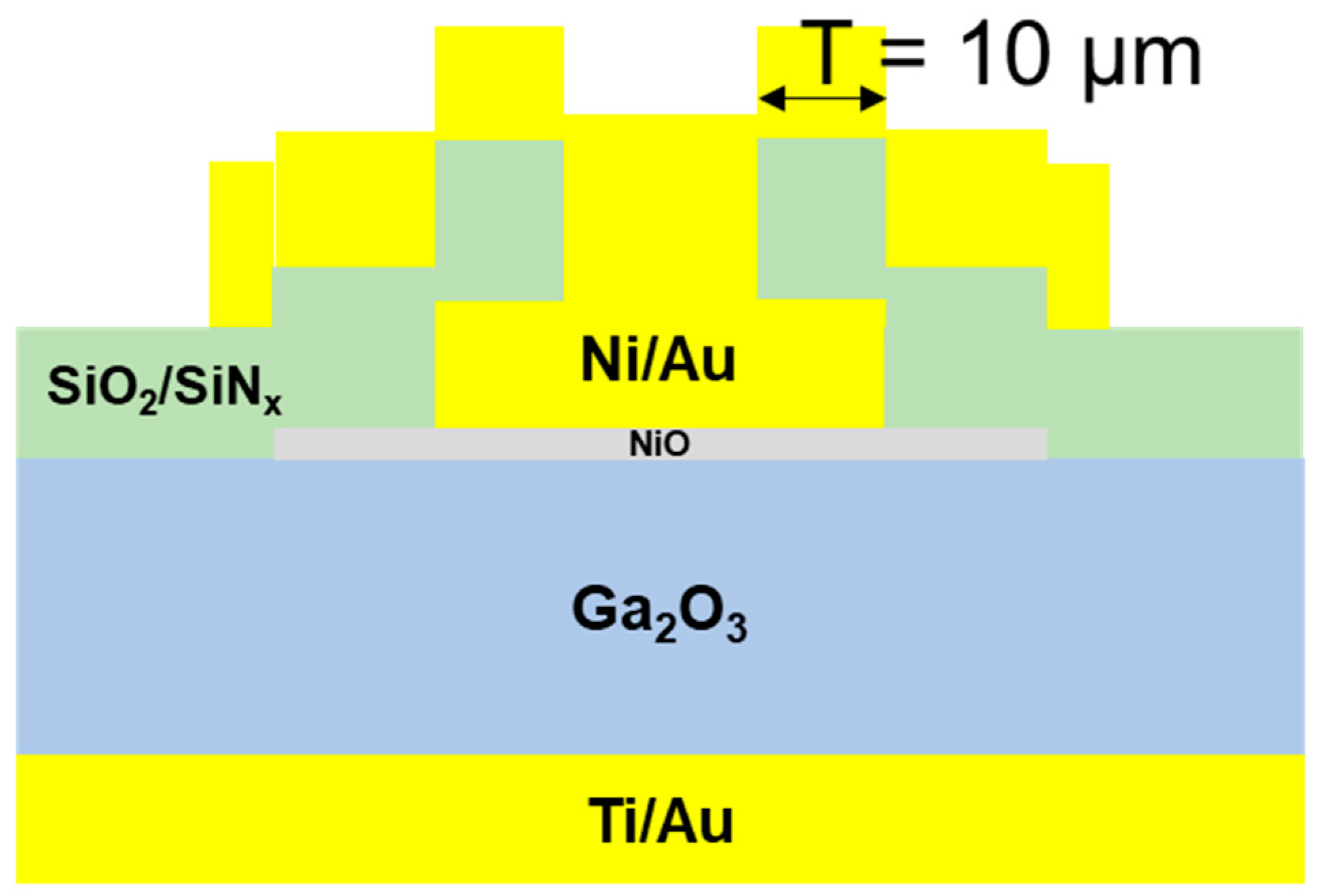
2. Materials and Methods
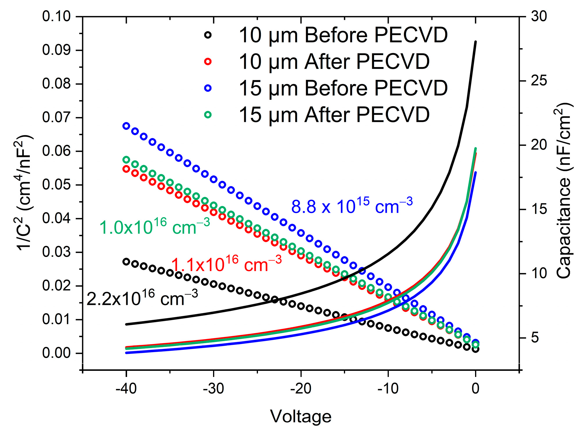
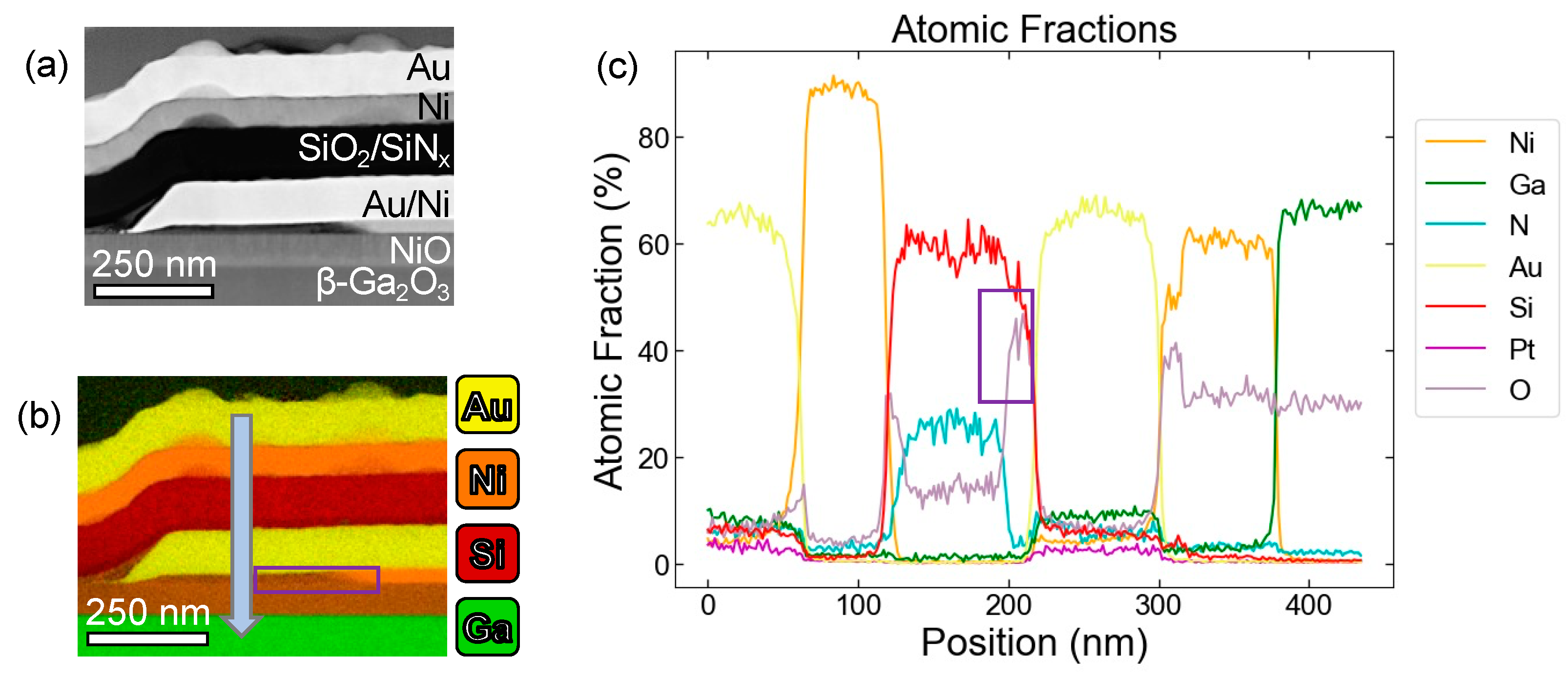
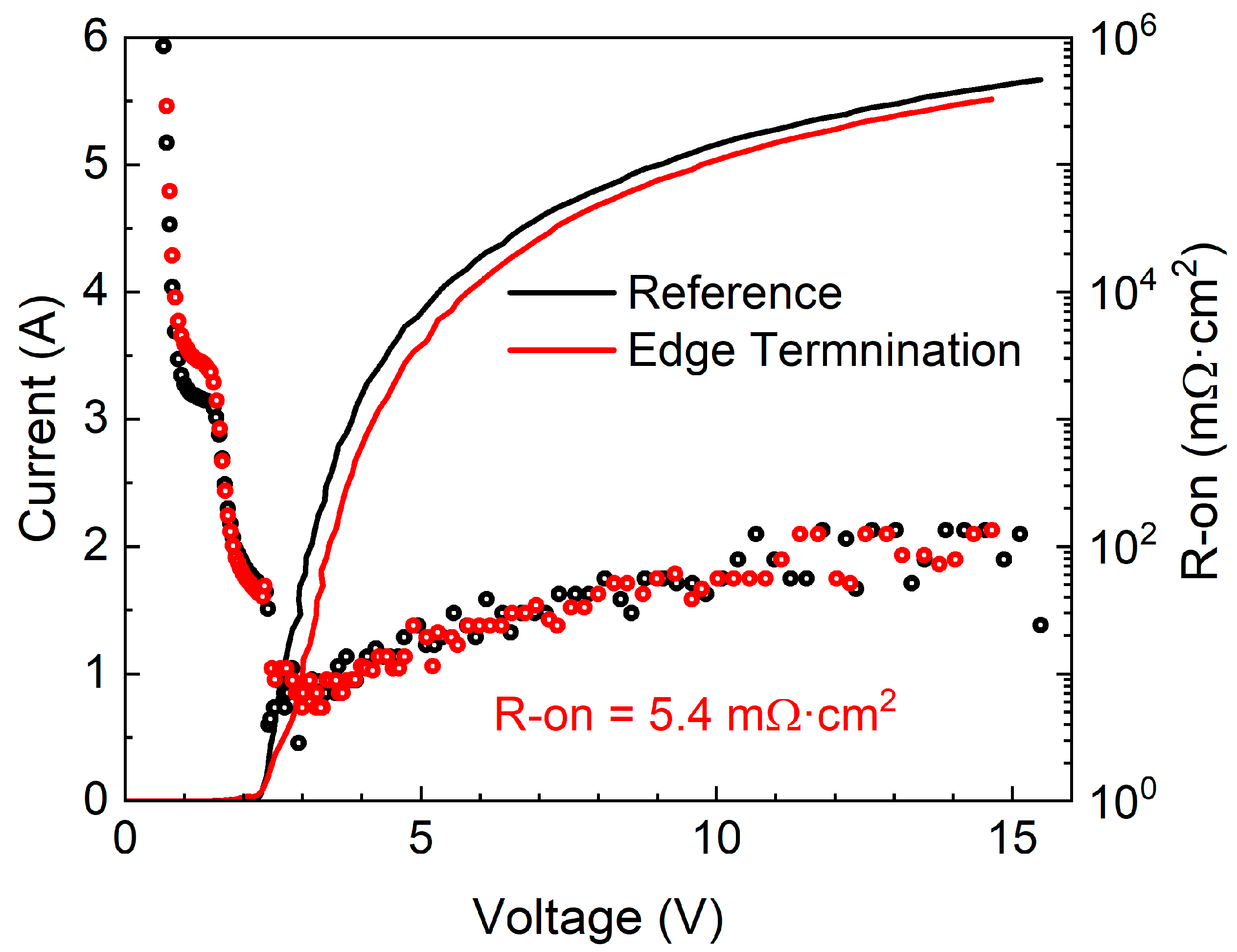
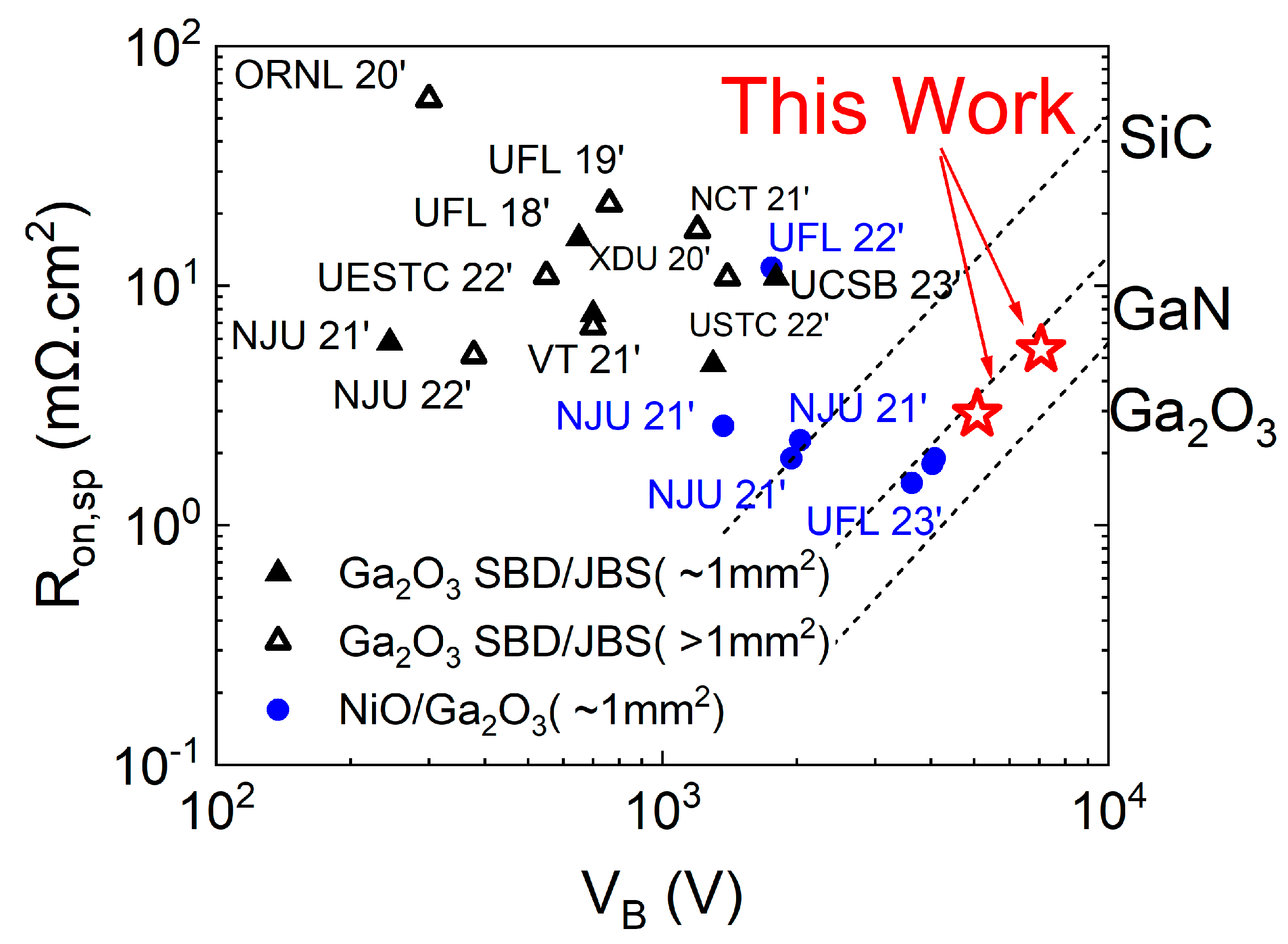
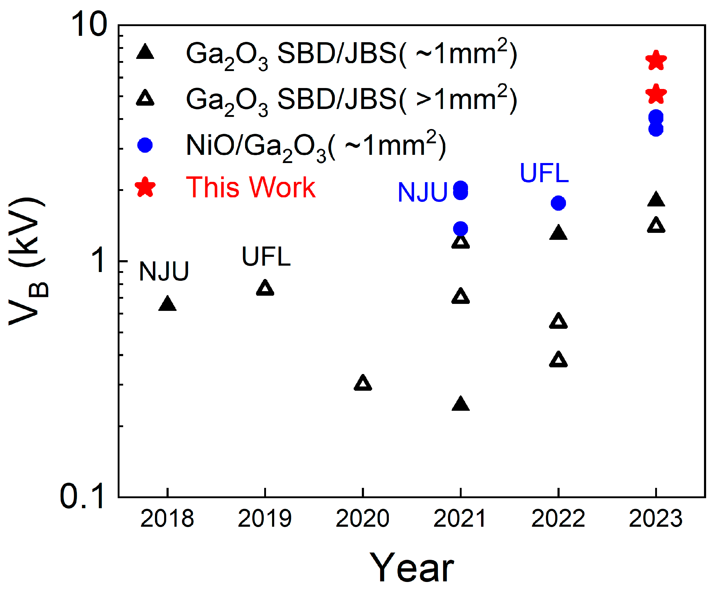
The drift region consists of either a 10 or 15 µm thick layer with light Si doping (8.8 × 10¹⁵–2.2 × 1016 cm−3) and was fabricated using halide vapor phase epitaxy (HVPE) on a (001) surface-oriented Sn-doped β-Ga2O3 single crystal obtained from Novel Crystal Technology, Japan. The net carrier densities in the drift layers were obtained from capacitance-voltage (C−V) measurements, as shown in Figure 1. We show the results both before and after the deposition of the dielectric field plates. The substrates manifest X-ray diffraction full width at half maximum values measuring less than 350 arc seconds in both the [100] and [010] directions. The rear-side Ohmic contact was established using an e-beam evaporated Ti/Au, with a combined thickness of 100 nm, and subjected to annealing at 550 °C for 60 s under N2 [10,32,33]. Figure 2 provides a schematic depiction of the vertical heterojunction rectifier structure. The edge termination consisted of bilayer SiNX/SiO2 field plates, as described in detail previously [53], and also a guard ring formed via extension of the NiO beyond the Ni/Au contact. The bilayer field plates were deposited via plasma-enhanced chemical vapor deposition (PECVD). The field plates extended 10 µm beyond the NiO, had 10 µm coverage over the NiAu contact, and extended 24 µm over the NiO.
The p-n heterojunction was formed via rf magnetron sputter deposition of a bilayer of NiO [34] at a working pressure of 3 mTorr with an 80 W power source. The deposition rate was deliberately set at 0.06 Å/sec, an intentionally slow rate to prevent any damage to the Ga2O3 surface. The bias voltage applied to the cathode of the sputtering system was approximately 50 V at 80 W power. It should be noted that at higher biases, visible lattice disorder has been observed via electron microscopy [10]. A two-layer structure with respective thicknesses of 20/10 nm and doping of 2.6 × 10¹⁸/1.0 × 1018 cm−3 was used. Detailed properties of the NiO material can be found in previous publications [34]. Electrical contact to the NiO was established via e-beam deposition of a total thickness of 100 nm of Ni/Au, with a contact diameter of 1 mm. Key points in the fabrication include minimizing damage to the interfaces with Ga2O3 and the NiO and SiNX/SiO2 layers.
A Ga-ion FEI Helios Nanolab 600I Dual Beam focused ion beam (FIB)/scanning electron microscopy (SEM) system was used to prepare lamella for scanning transmission electron microscopy (STEM) analysis (FEI Company, Hillsboro, OR, USA). The STEM analysis was performed using an aberration-corrected Themis Z equipped with a high-angle annular dark-field (HAADF) detector (FEI Company, Hillsboro, OR, USA) for Z-contrast imaging. The Themis Z is also equipped with a SuperX detector system to perform elemental analysis via energy-dispersive X-ray spectroscopy (EDS).
The current-voltage (I-V) characteristics were systematically measured under Fluorinert atmospheres at 25 °C using a Tektronix 371-B curve tracer and a Glassman high-voltage power supply. Additionally, an Agilent 4156C instrument was employed to capture low-voltage forward and reverse current characteristics. The reverse breakdown voltage was determined following the conventional definition, involving the measurement of reverse current reaching 1 mA/cm2. On-resistance was computed from the slope dV/dI of the I-V characteristics [7,9], adjusted for the resistance contributed by external circuit components, including cables, chuck, and probe, collectively amounting to 10 Ω. Calculated on-resistance values were predicated on the assumption of a current spreading length of 10 µm with a spreading angle of 45 degrees [17]. Typically, the reported RON corresponds to the unipolar drift resistance, which is generally smaller than the diffusion resistance. It is noteworthy that the I-V characteristics exhibited reproducibility over areas measuring 1 cm2 on the wafer, with absolute currents varying by no more than 20% at a given voltage.

3. Results

Figure 3a shows an HAADF-STEM image of all the layers in the final HJD device structure. Note that the Z-contrast characteristic in HAADF-STEM images makes certain layers appear much brighter or darker based on their relative atomic weight (e.g., brighter Au vs. darker Si). In Figure 3b, a colorized map using the results of an EDS scan shows the identified metallic and semiconducting species in the expected film stack arrangement. Figure 3c is an atomic fraction plot calculated along the light blue arrow in Figure 3b to identify the origin of the change in contrast in the first Ni metal layer. The change in contrast (location marked by the purple box in Figure 3b) can be explained by the unintentional oxidation of the Ni, as seen in the corresponding purple box in Figure 3c.
The forward I-V characteristics are shown in Figure 4 for the 1 mm diameter devices fabricated with the 15 µm drift layers and also with or without the field plate edge termination. The maximum forward current was 5.5 A, with 1 A reached at ~3 V forward, depending on the epi layer thickness. This shows the presence of the p-n junction does not prevent reaching high forward currents at moderate biases. The on-resistance was ~5.4 mΩ·cm−2 for the 15 µm layers. The forward currents were smaller for the thicker drift layers and at the expense of higher RON.
Figure 5 illustrates the reverse I-V characteristics of devices produced on 15 µm drift layers. Notably, these devices demonstrate breakthrough breakdown voltage (VB) values, reaching 7 kV, representing the highest reported values for large-area Ga2O3 rectifiers to date [1,5,20]. A summary of the VB values for the thick drift layers is given in Table 1. Note that the addition of the bilayer edge termination increases the VB from 5 to 7 kV. The reduction in the carrier concentration and thickness of the drift layer exerted a pronounced influence on VB, wherein devices characterized by higher doping or reduced thickness exhibited VB values approximately half those of devices with lower doping and increased thickness. For instance, devices manufactured on 10 µm drift layers demonstrated VB values within the range of 3.6–4 kV. The power figure of merit for the 7 kV devices was determined to be 9.2 GW·cm−2. This value corresponds to approximately 30% of the theoretical maximum for β-Ga2O3, underscoring the potential for further optimization in device design and material defect density [1,2,3,4,5].
The average electric field strength was 7 MV/cm, ~ 88% of the expected maximum near 8 MV·cm−1 and among the highest reported, particularly for large area devices [1,2,5,20]. It is noteworthy that in small diameter devices (100 µm) fabricated on the same wafers, we obtain breakdown voltages up to 12 kV. We ascribe this to the increased probability of having defects within the active region of the large area devices that contribute to reverse leakage current. There have been numerous studies to identify the crystal defects that contribute to reverse leakage current in Ga2O3 rectifiers. The leakage current can be ascribed to the existence of many types of such crystal defects in HVPE layers [54,55,56,57,58,59,60,61,62,63,64,65,66,67,68,69,70,71,72]. These include polycrystalline anomalies [65,72], stacking faults [66], probe-induced surface defects [67], line-shaped imperfections [68], ⟨1 3¯3¯ 2⟩ dislocations [69,70,71], and comet-shaped anomalies [72], all of which function as conduits for reverse leakage currents in the thick drift regions grown with halide vapor phase epitaxy on (001) β-Ga2O3 substrates for Schottky barrier diodes (SBDs). The reverse current density remained below 10–10 A·cm−2 up to −100 V. As documented in previous studies, multiple leakage current mechanisms are evident, encompassing variable range hopping and trap-assisted space-charge-limited current [15,22,37]. The former exhibits a linear correlation between ln(J)−E at lower biases, while at elevated voltages, a linear relationship is observed between ln (J)−ln (V).
To contextualize the present study, Figure 6 presents a compilation of reported specific Ron versus VB outcomes documented in the literature for rectifiers in the Ampere-class range. This compilation encompasses conventional Schottky barrier or JBS rectifiers, as well as NiO/Ga2O3 heterojunction rectifiers [22,25,29,30,31,33,35]. The theoretical lines representing the one 1D unipolar limits of SiC, GaN, and Ga2O3 are also included for reference. The findings of this investigation demonstrate the realization of large-area Ampere-class Ga2O3 rectifiers that surpass the theoretical limits established for GaN and SiC.
Figure 7 depicts a graph illustrating the rise in VB for large-area Ga2O3 rectifiers as a function of the publication date. The plot underscores the swift advancements in both growth and device technology pertaining to high-voltage Ga2O3 rectifiers. The findings presented in this current manuscript delineate the impact of augmenting the drift region thickness and optimizing device processing parameters on overall device performance. Notably, elevating the drift layer thickness from 10 to 15 µm resulted in a nearly 40% increase in VB.
Recently, an investigation was conducted into the elevated temperature characteristics of small-area NiO/Ga2O3 rectifiers. It was observed that these rectifiers demonstrate superior stability up to 600 K compared to Schottky rectifiers produced on identical wafers [17]. The investigated devices manifested breakdown fields of approximately 8.5 MV·cm−1, thereby establishing this value as a lower threshold for β-Ga2O3 [18,19]. Future research endeavors aim to extend analogous analyses to large-area devices.

4. Conclusions

In summary, we present the findings of our investigation involving large-area NiO/β-Ga2O3 p-n heterojunction rectifiers, characterized by VB of 7 kV, an on-state resistance (Ron) measuring 5.4 mΩ·cm2, and a figure-of-merit (VB2/Ron) reaching 9.2 GW·cm−2. Our results indicate that utilizing state-of-the-art thick epitaxial structures grown by HVPE and incorporating NiO as a p-layer to form a heterojunction with Ga2O3, a straightforward and planar fabrication approach yields performance metrics surpassing the one-dimensional (1D) unipolar characteristics of GaN and SiC. This outcome is particularly promising, given the additional advantages associated with Ga2O3, including cost-effectiveness and the availability of scalable bulk growth technology. An imperative avenue for future research lies in minimizing the deleterious effects caused by sputtering during NiO deposition, potentially via the utilization of direct metal-organic chemical vapor deposition (MOCVD) growth. Furthermore, there exists a need for deeper insights into edge termination techniques and potential influences of minority carrier effects on modulation [9].
In this investigation, we presented the synthesis and characterization of vertically aligned NiO/β polymorph n-Ga2O3/n+ Ga2O3 heterojunction rectifiers, featuring a substantial active area of 1 mm2. To enhance the VB, a dual-layer (SiNX/SiO2) dielectric field plate edge termination was employed. These heterojunction rectifiers demonstrate a remarkable simultaneous achievement of high breakdown voltage and substantial conducting currents. In particular, the devices exhibit a VB of 7 kV when employing a 15 µm thick drift layer with a doping concentration of 8.8 × 1015 cm−3, concurrently demonstrating a forward current of 5.5 A. The substantial thickness of the drift layer plays a pivotal role in achieving high VB, as evidenced by similar devices fabricated on 10 µm thick epilayers, which exhibited breakdown voltages in the range of 3.6–4.0 kV. Reference devices fabricated on 15 µm drift layers had a VB of 5 kV. It is noteworthy that the breakdown mechanism is attributed to leakage current from tunneling and thermionic emission, rather than avalanche breakdown. Evaluation of the power figure-of-merit, represented by VB2/RON, yielded a value of 9.2 GW·cm−2, where RON denotes the on-state resistance, measuring 5.4 mΩ·cm2. The capacitance per unit area (Coff) was determined to be 4 nF/cm2, resulting in an RON × Coff product of 34 ps and a cutoff frequency (FCO) of 29 GHz. The turn-on voltage for these rectifiers was approximately 2 V.
This exceptional performance surpasses the theoretical unipolar one-dimensional (1D) limit of both SiC and GaN, emphasizing the potential of β-Ga2O3 for forthcoming generations of high-power rectification devices. The presented results underscore the efficacy of the proposed heterojunction rectifier design, showcasing the viability of Gallium oxide in advancing the capabilities of high-power semiconductor devices beyond the limitations of conventional materials. The forward current-voltage (I-V) characteristics for the 1 mm diameter devices, fabricated with 15 µm thick drift layers, with and without the inclusion of a field plate edge termination showed the maximum forward current observed was 5.5 A, reaching 1 A at approximately 3 V forward bias, contingent upon the epitaxial layer thickness. This observation highlights that the presence of the p-n junction does not impede the attainment of high forward currents under moderate biases. The on-resistance was measured to be approximately 5.4 mΩ·cm−2 for the 15 µm thick layers. Notably, the forward currents were found to be larger for thicker drift layers, albeit at the expense of higher RON. The reverse current-voltage (I-V) characteristics for devices manufactured on 15 µm thick drift layers showed these devices exhibited breakthrough voltage values of 7 kV, representing the highest reported for large-area Ga2O3 rectifiers. The concise summary of the VB values for the thick drift layers presented in Table 1 showed that it is noteworthy that the incorporation of a bilayer edge termination enhances the VB from 5 to 7 kV. The alteration in drift layer carrier concentration and thickness significantly influences VB, with devices having higher doping or lower thickness displaying breakdown voltages approximately half of those observed in the lower-doped, thick devices. For instance, devices fabricated on 10 µm drift layers demonstrated VB values ranging from 3.6 to 4 kV. The power figure of merit for the 7 kV devices was determined to be 9.2 GW·cm−2, which accounts for approximately 30% of the theoretical maximum for β-Ga2O3. This observation suggests that there is room for optimization in terms of device design and material defect density. The average electric field strength was measured at 7 MV/cm, approximately 88% of the anticipated maximum near 8 MV·cm−1, and stands among the highest reported, particularly for large-area devices. It is noteworthy that in small-diameter devices (100 µm) fabricated on the same wafers, breakdown voltages of up to 12 kV were obtained. This is attributed to the increased likelihood of defects within the active region of large-area devices contributing to reverse leakage current.
Numerous studies have been conducted to identify crystal defects contributing to reverse leakage current in Ga2O3 rectifiers. The leakage current can be attributed to various crystal defects in HVPE layers, including polycrystalline anomalies, stacking faults, probe-induced surface defects, line-shaped imperfections, oriented dislocations, and comet-shaped anomalies. These defects serve as conduits for reverse leakage currents in the thick drift regions grown by halide vapor phase epitaxy on (001) β-Ga2O3 substrates for Schottky barrier diodes. The reverse current density up to −100 V was found to be <10−10 A·cm−2 at this voltage. Consistent with previous reports, several leakage current mechanisms are present, including variable range hopping and trap-assisted space-charge-limited current. The former exhibits a linear relationship of ln(J)−E at lower biases, while at higher voltages, there is a linear relationship of ln (J)–ln (V). In contextualizing the present work, a compilation of reported Ron (on-state resistance) versus VB (breakdown voltage) results for Ampere-class rectifiers from the literature shows the exceptional result reported in this manuscript. The dataset encompasses conventional Schottky barrier or JBS (Junction Barrier Schottky) rectifiers, as well as NiO/Ga2O3 heterojunction rectifiers. The theoretical limits for the one-dimensional (1D) unipolar performance of SiC, GaN, and Ga2O3 depicted for reference demonstrate the achievement of large-area, Ampere-class Ga2O3 rectifiers surpassing the theoretical limits of GaN and SiC. The progression of VB for large-area Ga2O3 rectifiers as a function of publication date highlights the rapid advancements in growth and device technology for high-voltage Ga2O3 rectifiers. The results presented in this manuscript underscore how increasing the drift region thickness and optimizing device processing parameters have contributed to notable improvements in device performance. For instance, the augmentation of the drift layer thickness from 10 to 15 µm resulted in a nearly 40% increase in VB. There is still much to optimize in terms of manufacturability, reliability, thermal management, and stability of the NiO before this technology is ready for deployment [7,73,74,75,76,77,78,79,80,81,82].

Author Contributions

Conceptualization, F.R.; methodology, F.R. and J.-S.L.; formal analysis, J.-S.L.; investigation, C.-C.C., J.-S.L., H.-H.W., T.J.Y. and H.K.; resources, F.R.; data curation, J.-S.L.; writing—original draft preparation, J.-S.L., T.J.Y. and H.K.; writing—review and editing, S.J.P.; visualization, J.-S.L.; supervision, F.R.; project administration, F.R.; funding acquisition, F.R. and S.J.P. All authors have read and agreed to the published version of the manuscript.

Funding

This research was funded by the Department of the Defense, Defense Threat Reduction Agency under award HDTRA1-20-2-0002. The work at UF was also supported by NSF DMR 1856662.

Data Availability Statement

The data that support the findings of this study are available within the article.

Acknowledgments

The work at UF was performed as part of the Interaction of Ionizing Radiation with Matter University Research Alliance (IIRM-URA), sponsored by the Department of the Defense, Defense Threat Reduction Agency under award HDTRA1-20-2-0002. The content of the information does not necessarily reflect the position or the policy of the federal government, and no official endorsement should be inferred. The work at UF was also supported by NSF DMR 1856662.

Conflicts of Interest

The authors declare no conflict of interest.

References

  1. Qin, Y.; Wang, Z.; Ye, J.; Zhang, Y. Recent progress of Ga2O3 power technology: Large-area devices, packaging, and applications. Jpn. J. Appl. Phys. 2023, 62, SF0801. [Google Scholar] [CrossRef]
  2. Wong, M.H.; Higashiwaki, M. Vertical β-Ga2O3 power transistors: A review. IEEE Trans. Electron Devices 2020, 67, 3925–3937. [Google Scholar] [CrossRef]
  3. Wong, M.H. High Breakdown Voltage β-Ga2O3 Schottky Diodes. In Ultrawide Bandgap β-Ga2O3 Semiconductor: Theory and Applications; AIP Publishing LLC: Melville, NY, USA, 2023. [Google Scholar]
  4. Green, A.J.; Speck, J.; Xing, G.; Moens, P.; Allerstam, F.; Gumaelius, K.; Neyer, T.; Arias-Purdue, A.; Mehrotra, V.; Kuramata, A. β-Gallium oxide power electronics. APL Mater. 2022, 10, 029201. [Google Scholar] [CrossRef]
  5. Lu, X.; Deng, Y.; Pei, Y.; Chen, Z.; Wang, G. Recent advances in NiO/Ga2O3 heterojunctions for power electronics. J. Semicond. 2023, 44, 061802. [Google Scholar] [CrossRef]
  6. Pearton, S.; Ren, F.; Tadjer, M.; Kim, J. Perspective: Ga2O3 for ultra-high power rectifiers and MOSFETS. J. Appl. Phys. 2018, 124, 220901. [Google Scholar]
  7. Wang, C.; Zhang, J.; Xu, S.; Zhang, C.; Feng, Q.; Zhang, Y.; Ning, J.; Zhao, S.; Zhou, H.; Hao, Y. Progress in state-of-the-art technologies of Ga2O3 devices. J. Phys. D Appl. Phys. 2021, 54, 243001. [Google Scholar] [CrossRef]
  8. Sharma, S.; Zeng, K.; Saha, S.; Singisetti, U. Field-plated lateral Ga2O3 MOSFETs with polymer passivation and 8.03 kV breakdown voltage. IEEE Electron Device Lett. 2020, 41, 836–839. [Google Scholar] [CrossRef]
  9. Zhang, J.; Dong, P.; Dang, K.; Zhang, Y.; Yan, Q.; Xiang, H.; Su, J.; Liu, Z.; Si, M.; Gao, J. Ultra-wide bandgap semiconductor Ga2O3 power diodes. Nat. Commun. 2022, 13, 3900. [Google Scholar] [CrossRef]
  10. Dong, P.; Zhang, J.; Yan, Q.; Liu, Z.; Ma, P.; Zhou, H.; Hao, Y. 6 kV/3.4 mΩ·cm2 vertical β-Ga2O3 Schottky barrier diode with BV 2/R on, sp performance exceeding 1-D unipolar limit of GaN and SiC. IEEE Electron Device Lett. 2022, 43, 765–768. [Google Scholar] [CrossRef]
  11. Li, J.-S.; Chiang, C.-C.; Xia, X.; Yoo, T.J.; Ren, F.; Kim, H.; Pearton, S. Demonstration of 4.7 kV breakdown voltage in NiO/β-Ga2O3 vertical rectifiers. Appl. Phys. Lett. 2022, 121, 042105. [Google Scholar] [CrossRef]
  12. Roy, S.; Bhattacharyya, A.; Ranga, P.; Splawn, H.; Leach, J.; Krishnamoorthy, S. High-k oxide field-plated vertical (001) β-Ga2O3 Schottky barrier diode with Baliga’s figure of merit over 1 GW/cm2. IEEE Electron Device Lett. 2021, 42, 1140–1143. [Google Scholar] [CrossRef]
  13. Bhattacharyya, A.; Sharma, S.; Alema, F.; Ranga, P.; Roy, S.; Peterson, C.; Seryogin, G.; Osinsky, A.; Singisetti, U.; Krishnamoorthy, S. 4.4 kV β-Ga2O3 MESFETs with power figure of merit exceeding 100 MW cm−2. Appl. Phys. Express 2022, 15, 061001. [Google Scholar] [CrossRef]
  14. Chabak, K.D.; Leedy, K.D.; Green, A.J.; Mou, S.; Neal, A.T.; Asel, T.; Heller, E.R.; Hendricks, N.S.; Liddy, K.; Crespo, A. Lateral β-Ga2O3 field effect transistors. Semicond. Sci. Technol. 2019, 35, 013002. [Google Scholar] [CrossRef]
  15. Hu, Z.; Nomoto, K.; Li, W.; Zhang, Z.; Tanen, N.; Thieu, Q.T.; Sasaki, K.; Kuramata, A.; Nakamura, T.; Jena, D. Breakdown mechanism in 1 kA/cm2 and 960 V E-mode β-Ga2O3 vertical transistors. Appl. Phys. Lett. 2018, 113, 122103. [Google Scholar] [CrossRef]
  16. Sharma, R.; Xian, M.; Fares, C.; Law, M.E.; Tadjer, M.; Hobart, K.D.; Ren, F.; Pearton, S.J. Effect of probe geometry during measurement of >100 A Ga2O3 vertical rectifiers. J. Vac. Sci. Technol. A 2021, 39, 013406. [Google Scholar] [CrossRef]
  17. Li, J.-S.; Chiang, C.-C.; Xia, X.; Wan, H.-H.; Ren, F.; Pearton, S. Superior high temperature performance of 8 kV NiO/Ga2O3 vertical heterojunction rectifiers. J. Mater. Chem. C 2023, 11, 7750–7757. [Google Scholar] [CrossRef]
  18. Li, J.-S.; Wan, H.-H.; Chiang, C.-C.; Xia, X.; Yoo, T.J.; Kim, H.; Ren, F.; Pearton, S.J. Reproducible NiO/Ga2O3 Vertical Rectifiers with Breakdown Voltage> 8 kV. Crystals 2023, 13, 886. [Google Scholar] [CrossRef]
  19. Li, J.-S.; Chiang, C.-C.; Xia, X.; Wan, H.-H.; Ren, F.; Pearton, S. Effect of drift layer doping and NiO parameters in achieving 8.9 kV breakdown in 100 μm diameter and 4 kV/4 A in 1 mm diameter NiO/β-Ga2O3 rectifiers. J. Vac. Sci. Technol. A 2023, 41, 043404. [Google Scholar] [CrossRef]
  20. Wong, M.H. A landscape of β-Ga2O3 Schottky power diodes. J. Semicond. 2023, 44, 1–10. [Google Scholar] [CrossRef]
  21. Gong, H.; Zhou, F.; Xu, W.; Yu, X.; Xu, Y.; Yang, Y.; Ren, F.-F.; Gu, S.; Zheng, Y.; Zhang, R. 1.37 kV/12 A NiO/β-Ga2O3 heterojunction diode with nanosecond reverse recovery and rugged surge-current capability. IEEE Trans. Power Electron. 2021, 36, 12213–12217. [Google Scholar] [CrossRef]
  22. Ji, M.; Taylor, N.R.; Kravchenko, I.; Joshi, P.; Aytug, T.; Cao, L.R.; Paranthaman, M.P. Demonstration of large-size vertical Ga2O3 Schottky barrier diodes. IEEE Trans. Power Electron. 2020, 36, 41–44. [Google Scholar] [CrossRef]
  23. Yang, J.; Fares, C.; Elhassani, R.; Xian, M.; Ren, F.; Pearton, S.; Tadjer, M.; Kuramata, A. Reverse breakdown in large area, field-plated, vertical β-Ga2O3 rectifiers. ECS J. Solid State Sci. Technol. 2019, 8, Q3159. [Google Scholar] [CrossRef]
  24. Yang, J.; Ren, F.; Tadjer, M.; Pearton, S.; Kuramata, A. Ga2O3 Schottky rectifiers with 1 ampere forward current, 650 V reverse breakdown and 26.5 MW·cm−2 figure-of-merit. AIP Adv. 2018, 8, 055026. [Google Scholar] [CrossRef]
  25. Xiao, M.; Wang, B.; Liu, J.; Zhang, R.; Zhang, Z.; Ding, C.; Lu, S.; Sasaki, K.; Lu, G.-Q.; Buttay, C. Packaged Ga2O3 Schottky rectifiers with over 60-A surge current capability. IEEE Trans. Power Electron. 2021, 36, 8565–8569. [Google Scholar] [CrossRef]
  26. Gong, H.; Zhou, F.; Yu, X.; Xu, W.; Ren, F.-F.; Gu, S.; Lu, H.; Ye, J.; Zhang, R. 70-μm-body Ga2O3 Schottky barrier diode with 1.48 K/W thermal resistance, 59 A surge current and 98.9% conversion efficiency. IEEE Electron Device Lett. 2022, 43, 773–776. [Google Scholar] [CrossRef]
  27. Otsuka, F.; Miyamoto, H.; Takatsuka, A.; Kunori, S.; Sasaki, K.; Kuramata, A. Large-size (1.7× 1.7 mm2) β-Ga2O3 field-plated trench MOS-type Schottky barrier diodes with 1.2 kV breakdown voltage and 109 high on/off current ratio. Appl. Phys. Express 2021, 15, 016501. [Google Scholar] [CrossRef]
  28. Hao, W.; Wu, F.; Li, W.; Xu, G.; Xie, X.; Zhou, K.; Guo, W.; Zhou, X.; He, Q.; Zhao, X. High-performance vertical β-Ga2O3 Schottky barrier diodes featuring P-NiO JTE with adjustable conductivity. In Proceedings of the 2022 International Electron Devices Meeting (IEDM), San Francisco, CA, USA, 3–7 December 2022; pp. 9.5.1–9.5.4. [Google Scholar]
  29. Lv, Y.; Wang, Y.; Fu, X.; Dun, S.; Sun, Z.; Liu, H.; Zhou, X.; Song, X.; Dang, K.; Liang, S. Demonstration of β-Ga2O3 junction barrier Schottky diodes with a Baliga′s figure of merit of 0.85 GW/cm2 or a 5A/700 V handling capabilities. IEEE Trans. Power Electron. 2020, 36, 6179–6182. [Google Scholar] [CrossRef]
  30. Wei, J.; Wei, Y.; Lu, J.; Peng, X.; Jiang, Z.; Yang, K.; Luo, X. Experimental Study on Electrical Characteristics of Large-Size Vertical β-Ga2O3 Junction Barrier Schottky Diodes. In Proceedings of the 2022 IEEE 34th International Symposium on Power Semiconductor Devices and ICs (ISPSD), Vancouver, BC, Canada, 22–25 May 2022; pp. 97–100. [Google Scholar]
  31. Zhou, F.; Gong, H.; Wang, Z.; Xu, W.; Yu, X.; Yang, Y.; Ren, F.-F.; Gu, S.; Zhang, R.; Zheng, Y. Over 1.8 GW/cm2 beveled-mesa NiO/β-Ga2O3 heterojunction diode with 800 V/10 A nanosecond switching capability. Appl. Phys. Lett. 2021, 119, 262103. [Google Scholar] [CrossRef]
  32. Zhou, F.; Gong, H.; Xu, W.; Yu, X.; Xu, Y.; Yang, Y.; Ren, F.-F.; Gu, S.; Zheng, Y.; Zhang, R. 1.95-kV beveled-mesa NiO/β-Ga2O3 heterojunction diode with 98.5% conversion efficiency and over million-times overvoltage ruggedness. IEEE Trans. Power Electron. 2021, 37, 1223–1227. [Google Scholar] [CrossRef]
  33. Li, J.-S.; Chiang, C.-C.; Xia, X.; Tsai, C.-T.; Ren, F.; Liao, Y.-T.; Pearton, S. Dynamic Switching of 1.9 A/1.76 kV Forward Current NiO/β-Ga2O3 Rectifiers. ECS J. Solid State Sci. Technol. 2022, 11, 105003. [Google Scholar] [CrossRef]
  34. Li, J.-S.; Xia, X.; Chiang, C.-C.; Hays, D.C.; Gila, B.P.; Craciun, V.; Ren, F.; Pearton, S. Deposition of sputtered NiO as a p-type layer for heterojunction diodes with Ga2O3. J. Vac. Sci. Technol. A 2023, 41, 013405. [Google Scholar] [CrossRef]
  35. Li, J.-S.; Chiang, C.-C.; Xia, X.; Wan, H.-H.; Ren, F.; Pearton, S. 1 mm2, 3.6 kV, 4.8 A NiO/Ga2O3 Heterojunction Rectifiers. ECS J. Solid State Sci. Technol. 2023, 12, 085001. [Google Scholar] [CrossRef]
  36. Roy, S. Ultra-Low Reverse Leakage in Large Area Kilo-Volt class β-Ga2O3 Trench Schottky Barrier Diode with High-k Dielectric RESURF. TechRxiv 2023. [Google Scholar] [CrossRef]
  37. Li, W.; Saraswat, D.; Long, Y.; Nomoto, K.; Jena, D.; Xing, H.G. Near-ideal reverse leakage current and practical maximum electric field in β-Ga2O3 Schottky barrier diodes. Appl. Phys. Lett. 2020, 116, 192101. [Google Scholar] [CrossRef]
  38. Lu, X.; Zhou, X.; Jiang, H.; Ng, K.W.; Chen, Z.; Pei, Y.; Lau, K.M.; Wang, G. 1-kV Sputtered p-NiO/n-Ga2O3 Heterojunction Diodes With an Ultra-Low Leakage Current Below 1 μA/cm2. IEEE Electron Device Lett. 2020, 41, 449–452. [Google Scholar] [CrossRef]
  39. Chi, Z.; Asher, J.J.; Jennings, M.R.; Chikoidze, E.; Pérez-Tomás, A. Ga2O3 and related ultra-wide bandgap power semiconductor oxides: New energy electronics solutions for CO2 emission mitigation. Materials 2022, 15, 1164. [Google Scholar] [CrossRef]
  40. Wang, C.; Gong, H.; Lei, W.; Cai, Y.; Hu, Z.; Xu, S.; Liu, Z.; Feng, Q.; Zhou, H.; Ye, J. Demonstration of the p-NiOx/n-Ga2O3 heterojunction gate FETs and diodes with BV2/R on, sp figures of merit of 0.39 GW/cm2 and 1.38 GW/cm2. IEEE Electron Device Lett. 2021, 42, 485–488. [Google Scholar] [CrossRef]
  41. Yan, Q.; Gong, H.; Zhou, H.; Zhang, J.; Ye, J.; Liu, Z.; Wang, C.; Zheng, X.; Zhang, R.; Hao, Y. Low density of interface trap states and temperature dependence study of Ga2O3 Schottky barrier diode with p-NiOx termination. Appl. Phys. Lett. 2022, 120, 092106. [Google Scholar] [CrossRef]
  42. Gong, H.; Chen, X.; Xu, Y.; Ren, F.-F.; Gu, S.; Ye, J. A 1.86-kV double-layered NiO/β-Ga2O3 vertical p–n heterojunction diode. Appl. Phys. Lett. 2020, 117, 022104. [Google Scholar] [CrossRef]
  43. Gong, H.; Yu, X.; Xu, Y.; Chen, X.; Kuang, Y.; Lv, Y.; Yang, Y.; Ren, F.-F.; Feng, Z.; Gu, S. β-Ga2O3 vertical heterojunction barrier Schottky diodes terminated with p-NiO field limiting rings. Appl. Phys. Lett. 2021, 118, 202102. [Google Scholar] [CrossRef]
  44. Hao, W.; He, Q.; Zhou, K.; Xu, G.; Xiong, W.; Zhou, X.; Jian, G.; Chen, C.; Zhao, X.; Long, S. Low defect density and small I–V curve hysteresis in NiO/β-Ga2O3 pn diode with a high PFOM of 0.65 GW/cm2. Appl. Phys. Lett. 2021, 118, 043501. [Google Scholar] [CrossRef]
  45. Xia, X.; Li, J.-S.; Chiang, C.-C.; Yoo, T.J.; Ren, F.; Kim, H.; Pearton, S. Annealing temperature dependence of band alignment of NiO/β-Ga2O3. J. Phys. D Appl. Phys. 2022, 55, 385105. [Google Scholar] [CrossRef]
  46. Zhang, J.; Han, S.; Cui, M.; Xu, X.; Li, W.; Xu, H.; Jin, C.; Gu, M.; Chen, L.; Zhang, K.H. Fabrication and interfacial electronic structure of wide bandgap NiO and Ga2O3 p–n heterojunction. ACS Appl. Electron. Mater. 2020, 2, 456–463. [Google Scholar] [CrossRef]
  47. Wang, Y.; Gong, H.; Lv, Y.; Fu, X.; Dun, S.; Han, T.; Liu, H.; Zhou, X.; Liang, S.; Ye, J. 2.41 kV Vertical P-Nio/n-Ga2O3 Heterojunction Diodes With a Record Baliga’s Figure-of-Merit of 5.18 GW/cm2. IEEE Trans. Power Electron. 2021, 37, 3743–3746. [Google Scholar] [CrossRef]
  48. Zhou, H.; Zeng, S.; Zhang, J.; Liu, Z.; Feng, Q.; Xu, S.; Zhang, J.; Hao, Y. Comprehensive study and optimization of implementing p-NiO in β-Ga2O3 based diodes via TCAD simulation. Crystals 2021, 11, 1186. [Google Scholar] [CrossRef]
  49. Yang, J.; Xian, M.; Carey, P.; Fares, C.; Partain, J.; Ren, F.; Tadjer, M.; Anber, E.; Foley, D.; Lang, A. Vertical geometry 33.2 A, 4.8 MW cm2 Ga2O3 field-plated Schottky rectifier arrays. Appl. Phys. Lett. 2019, 114, 232106. [Google Scholar] [CrossRef]
  50. Yang, J.; Ren, F.; Chen, Y.-T.; Liao, Y.-T.; Chang, C.-W.; Lin, J.; Tadjer, M.J.; Pearton, S.; Kuramata, A. Dynamic Switching Characteristics of 1 A Forward Current β-Ga2O3 Rectifiers. IEEE J. Electron Devices Soc. 2018, 7, 57–61. [Google Scholar] [CrossRef]
  51. Li, J.-S.; Chiang, C.-C.; Xia, X.; Ren, F.; Pearton, S. Temperature dependence of on–off ratio and reverse recovery time in NiO/β-Ga2O3 heterojunction rectifiers. J. Vac. Sci. Technol. A 2022, 40, 063407. [Google Scholar] [CrossRef]
  52. Hao, W.; He, Q.; Han, Z.; Zhao, X.; Xu, G.; Yang, S.; Long, S. 1 kV Vertical β-Ga2O3 Heterojunction Barrier Schottky Diode with Hybrid Unipolar and Bipolar Operation. In Proceedings of the 2023 35th International Symposium on Power Semiconductor Devices and ICs (ISPSD), Hong Kong, China, 28 May–1 June 2023; pp. 394–397. [Google Scholar]
  53. Carey, P.H.; Yang, J.; Ren, F.; Sharma, R.; Law, M.; Pearton, S.J. Comparison of dual-stack dielectric field plates on β-Ga2O3 Schottky rectifiers. ECS J. Solid State Sci. Technol. 2019, 8, Q3221. [Google Scholar] [CrossRef]
  54. Sdoeung, S.; Otsubo, Y.; Sasaki, K.; Kuramata, A.; Kasu, M. Killer defect responsible for reverse leakage current in halide vapor phase epitaxial (011) β-Ga2O3 Schottky barrier diodes investigated via ultrahigh sensitive emission microscopy and synchrotron x-ray topography. Appl. Phys. Lett. 2023, 123, 122101. [Google Scholar] [CrossRef]
  55. Chaman, M.I.; Hoshikawa, K.; Sdoeung, S.; Kasu, M. High crystal quality of vertical Bridgman and edge-defined film-fed growth β-Ga2O3 bulk crystals investigated using high-resolution X-ray diffraction and synchrotron X-ray topography. Jpn. J. Appl. Phys. 2022, 61, 055501. [Google Scholar] [CrossRef]
  56. Kasu, M.; Hanada, K.; Moribayashi, T.; Hashiguchi, A.; Oshima, T.; Oishi, T.; Koshi, K.; Sasaki, K.; Kuramata, A.; Ueda, O. Relationship between crystal defects and leakage current in β-Ga2O3 Schottky barrier diodes. Jpn. J. Appl. Phys. 2016, 55, 1202BB. [Google Scholar] [CrossRef]
  57. Kasu, M.; Oshima, T.; Hanada, K.; Moribayashi, T.; Hashiguchi, A.; Oishi, T.; Koshi, K.; Sasaki, K.; Kuramata, A.; Ueda, O. Crystal defects observed by the etch-pit method and their effects on Schottky-barrier-diode characteristics on β-Ga2O3. Jpn. J. Appl. Phys. 2017, 56, 091101. [Google Scholar] [CrossRef]
  58. Oshima, T.; Hashiguchi, A.; Moribayashi, T.; Koshi, K.; Sasaki, K.; Kuramata, A.; Ueda, O.; Oishi, T.; Kasu, M. Electrical properties of Schottky barrier diodes fabricated on (001) β-Ga2O3 substrates with crystal defects. Jpn. J. Appl. Phys. 2017, 56, 086501. [Google Scholar] [CrossRef]
  59. Ueda, O.; Ikenaga, N.; Koshi, K.; Iizuka, K.; Kuramata, A.; Hanada, K.; Moribayashi, T.; Yamakoshi, S.; Kasu, M. Structural evaluation of defects in β-Ga2O3 single crystals grown by edge-defined film-fed growth process. Jpn. J. Appl. Phys. 2016, 55, 1202BD. [Google Scholar] [CrossRef]
  60. Masuya, S.; Sasaki, K.; Kuramata, A.; Yamakoshi, S.; Ueda, O.; Kasu, M. Characterization of crystalline defects in β-Ga2O3 single crystals grown by edge-defined film-fed growth and halide vapor-phase epitaxy using synchrotron X-ray topography. Jpn. J. Appl. Phys. 2019, 58, 055501. [Google Scholar] [CrossRef]
  61. Hanada, K.; Moribayashi, T.; Uematsu, T.; Masuya, S.; Koshi, K.; Sasaki, K.; Kuramata, A.; Ueda, O.; Kasu, M. Observation of nanometer-sized crystalline grooves in as-grown β-Ga2O3 single crystals. Jpn. J. Appl. Phys. 2016, 55, 030303. [Google Scholar] [CrossRef]
  62. Hanada, K.; Moribayashi, T.; Koshi, K.; Sasaki, K.; Kuramata, A.; Ueda, O.; Kasu, M. Origins of etch pits in β-Ga2O3 (010) single crystals. Jpn. J. Appl. Phys. 2016, 55, 1202BG. [Google Scholar] [CrossRef]
  63. Ohba, E.; Kobayashi, T.; Kado, M.; Hoshikawa, K. Defect characterization of β-Ga2O3 single crystals grown by vertical Bridgman method. Jpn. J. Appl. Phys. 2016, 55, 1202BF. [Google Scholar] [CrossRef]
  64. Ueda, O.; Kasu, M.; Yamaguchi, H. Structural characterization of defects in EFG-and HVPE-grown β-Ga2O3 crystals. Jpn. J. Appl. Phys. 2022, 61, 050101. [Google Scholar] [CrossRef]
  65. Sdoeung, S.; Sasaki, K.; Kawasaki, K.; Hirabayashi, J.; Kuramata, A.; Oishi, T.; Kasu, M. Origin of reverse leakage current path in edge-defined film-fed growth (001) β-Ga2O3 Schottky barrier diodes observed by high-sensitive emission microscopy. Appl. Phys. Lett. 2020, 117, 022106. [Google Scholar] [CrossRef]
  66. Sdoeung, S.; Sasaki, K.; Kawasaki, K.; Hirabayashi, J.; Kuramata, A.; Kasu, M. Polycrystalline defects—Origin of leakage current—In halide vapor phase epitaxial (001) β-Ga2O3 Schottky barrier diodes identified via ultrahigh sensitive emission microscopy and synchrotron X-ray topography. Appl. Phys. Express 2021, 14, 036502. [Google Scholar] [CrossRef]
  67. Sdoeung, S.; Sasaki, K.; Masuya, S.; Kawasaki, K.; Hirabayashi, J.; Kuramata, A.; Kasu, M. Stacking faults: Origin of leakage current in halide vapor phase epitaxial (001) β-Ga2O3 Schottky barrier diodes. Appl. Phys. Lett. 2021, 118, 172106. [Google Scholar] [CrossRef]
  68. Sdoeung, S.; Sasaki, K.; Kawasaki, K.; Hirabayashi, J.; Kuramata, A.; Kasu, M. Probe-induced surface defects: Origin of leakage current in halide vapor-phase epitaxial (001) β-Ga2O3 Schottky barrier diodes. Appl. Phys. Lett. 2022, 120, 092101. [Google Scholar] [CrossRef]
  69. Sdoeung, S.; Sasaki, K.; Kawasaki, K.; Hirabayashi, J.; Kuramata, A.; Oishi, T.; Kasu, M. Line-shaped defects: Origin of leakage current in halide vapor-phase epitaxial (001) β-Ga2O3 Schottky barrier diodes. Appl. Phys. Lett. 2022, 120, 122107. [Google Scholar] [CrossRef]
  70. Sdoeung, S.; Sasaki, K.; Kuramata, A.; Kasu, M. Identification of dislocation responsible for leakage current in halide vapor phase epitaxial (001) β-Ga2O3 Schottky barrier diodes investigated via ultrahigh-sensitive emission microscopy and synchrotron X-ray topography. Appl. Phys. Express 2022, 15, 111001. [Google Scholar] [CrossRef]
  71. Sdoeung, S.; Sasaki, K.; Kawasaki, K.; Hirabayashi, J.; Kuramata, A.; Kasu, M. Characterization of dislocation of halide vapor phase epitaxial (001) β-Ga2O3 by ultrahigh sensitive emission microscopy and synchrotron X-ray topography and its influence on Schottky barrier diodes. Jpn. J. Appl. Phys. 2023, 62, SF1001. [Google Scholar] [CrossRef]
  72. Sdoeung, S.; SASAKI, k.; Kawasaki, K.; Hirabayashi, J.; Kuramata, A.; Kasu, M. Observation of comet-shaped defect as killer defect in halide vapor phase epitaxial (001) β-Ga2O3 and its impact on Schottky barrier diodes. Jpn. J. Appl. Phys. 2023, 62, 071001. [Google Scholar] [CrossRef]
  73. Guo, W.; Han, Z.; Zhao, X.; Xu, G.; Long, S. Large-area β-Ga2O3 Schottky barrier diode and its application in DC–DC converters. J. Semicond. 2023, 44, 072805. [Google Scholar] [CrossRef]
  74. Hao, W.; Wu, F.; Li, W.; Xu, G.; Xie, X.; Zhou, K.; Guo, W.; Zhou, X.; He, Q.; Zhao, X. Improved Vertical β-Ga2O3 Schottky Barrier Diodes With Conductivity-Modulated p-NiO Junction Termination Extension. IEEE Trans. Electron Devices 2023, 70, 2129–2134. [Google Scholar] [CrossRef]
  75. Liu, A.-C.; Hsieh, C.-H.; Langpoklakpam, C.; Singh, K.J.; Lee, W.-C.; Hsiao, Y.-K.; Horng, R.-H.; Kuo, H.-C.; Tu, C.-C. State-of-the-Art β-Ga2O3 Field-Effect Transistors for Power Electronics. ACS Omega 2022, 7, 36070–36091. [Google Scholar] [CrossRef]
  76. Ping, L.K.; Berhanuddin, D.D.; Mondal, A.K.; Menon, P.S.; Mohamed, M.A. Properties and perspectives of ultrawide bandgap Ga2O3 in optoelectronic applications. Chin. J. Phys. 2021, 73, 195–212. [Google Scholar] [CrossRef]
  77. Reese, S.B.; Remo, T.; Green, J.; Zakutayev, A. How much will gallium oxide power electronics cost? Joule 2019, 3, 903–907. [Google Scholar] [CrossRef]
  78. Sheoran, H.; Kumar, V.; Singh, R. A comprehensive review on recent developments in ohmic and Schottky contacts on Ga2O3 for device applications. ACS Appl. Electron. Mater. 2022, 4, 2589–2628. [Google Scholar] [CrossRef]
  79. Wang, B.; Xiao, M.; Spencer, J.; Qin, Y.; Sasaki, K.; Tadjer, M.J.; Zhang, Y. 2.5 kV Vertical Ga2O3 Schottky Rectifier with Graded Junction Termination Extension. IEEE Electron Device Lett. 2022, 44, 221–224. [Google Scholar] [CrossRef]
  80. Wei, Y.; Peng, X.; Jiang, Z.; Sun, T.; Wei, J.; Yang, K.; Hao, L.; Luo, X. Low Reverse Conduction Loss β-Ga2O3 Vertical FinFET With an Integrated Fin Diode. IEEE Trans. Electron Devices 2023, 70, 3454–3461. [Google Scholar] [CrossRef]
  81. Wu, F.; Wang, Y.; Jian, G.; Xu, G.; Zhou, X.; Guo, W.; Du, J.; Liu, Q.; Dun, S.; Yu, Z. Superior Performance β-Ga2O3 Junction Barrier Schottky Diodes Implementing p-NiO Heterojunction and Beveled Field Plate for Hybrid Cockcroft–Walton Voltage Multiplier. IEEE Trans. Electron Devices 2023, 70, 1199–1205. [Google Scholar] [CrossRef]
  82. Zhou, H.; Zhang, J.; Zhang, C.; Feng, Q.; Zhao, S.; Ma, P.; Hao, Y. A review of the most recent progresses of state-of-art gallium oxide power devices. J. Semicond. 2019, 40, 011803. [Google Scholar] [CrossRef]
Figure 1. C-V plots to determine carrier density in the drift regions.
Crystals 13 01624 g001
Figure 2. Schematic of large diameter HJD showing p-type NiO layer and SiNX/SiO2 edge termination.
Crystals 13 01624 g002
Figure 3. (a) HAADF-STEM image showing all the layers in the HJD with labels corresponding to the schematic in Figure 2. The topmost layer is an amorphous Pt strap deposited in the FIB to protect the sample surface during lamella preparation. (b) Colorized map of only the metallic and semiconducting species in the field of view of (a) using EDS elemental analysis. (c) Atomic fraction plot along the light blue arrow drawn in (b).
Crystals 13 01624 g003
Figure 4. Forward I-V characteristics from 1 mm2 HJDs fabricated on 15 µm drift layers.
Crystals 13 01624 g004
Figure 5. Reverse I-V characteristics at high bias from 1 mm2 HJDs fabricated on 15 µm drift layers.
Crystals 13 01624 g005
Figure 6. Compilation plot of Ron vs. VB from the reported literature of large area Ga2O3 HJDs and SBDs.
Crystals 13 01624 g006
Figure 7. Plot of VB versus year for large diameter (≥1 mm2) Ga2O3 SBDs and HJDs.
Crystals 13 01624 g007
Table 1. Breakdown voltages for 1 mm2 rectifiers with 15 µm thick drift layers. Reference is the breakdown without edge termination.
ReferenceEdge Termination
VB (V)50827063
RON (mΩ·cm−2)4.45.4
BFOM (GW·cm−2)5.79.2
Disclaimer/Publisher’s Note: The statements, opinions and data contained in all publications are solely those of the individual author(s) and contributor(s) and not of MDPI and/or the editor(s). MDPI and/or the editor(s) disclaim responsibility for any injury to people or property resulting from any ideas, methods, instructions or products referred to in the content.

