Article

Optical Absorption, Photocarrier Recombination Dynamics and Terahertz Dielectric Properties of Electron-Irradiated GaSe Crystals

by
Svetlana A. Bereznaya
1,
Ruslan A. Redkin
1,2,
Valentin N. Brudnyi
3,
Yury S. Sarkisov
4,
Xinyang Su
5,* and
Sergey Yu. Sarkisov
1,2,*
1
Laboratory for Terahertz Research, Tomsk State University, 634050 Tomsk, Russia
2
Synchrotron Radiation Detector Laboratory, R&D Center “Advanced Electronic Technologies”, Tomsk State University, 634050 Tomsk, Russia
3
Department of Semiconductor Physics, Tomsk State University, 634050 Tomsk, Russia
4
Department of Physics, Chemistry and Theoretical Mechanics, Tomsk State University of Architecture and Building, 634003 Tomsk, Russia
5
School of Physical Science and Engineering, Beijing Jiaotong University, Beijing 100044, China
*
Authors to whom correspondence should be addressed.
Crystals 2023, 13(11), 1562; https://doi.org/10.3390/cryst13111562
Submission received: 13 October 2023 / Revised: 30 October 2023 / Accepted: 30 October 2023 / Published: 1 November 2023
(This article belongs to the Special Issue Advances of Nonlinear Optical Materials)

Abstract

:
Optical absorption spectra of 9 MeV electron-irradiated GaSe crystals were studied. Two absorption bands with the low-photon-energy threshold at 1.35 and 1.73 eV (T = 300 K) appeared in the transparency region of GaSe after the high-energy-electron irradiation. The observed absorption bands were attributed to the defect states induced by Ga vacancies in two charge states, having the energy positions at 0.23 and 0.61 eV above the valence band maximum at T = 300 K. The optical pump-terahertz probe technique (OPTP) was employed to study the dark and photoexcited terahertz conductivity and charge carrier recombination dynamics at two-photon excitation of as-grown and 9 MeV electron-irradiated GaSe crystals. The measured values of the differential terahertz transmission at a specified photoexcitation condition were used to extract the terahertz charge carrier mobilities. The determined terahertz charge carrier mobility values were ~46 cm2/V·s and ~14 cm2/V·s for as-grown and heavily electron-irradiated GaSe crystals, respectively. These are quite close to the values determined from the Lorentz–Drude–Smith fitting of the measured dielectric constant spectra. The photo-injection-level-dependent charge carrier lifetimes were determined from the measured OPTP data, bearing in mind the model injection-level dependencies of the recombination rates governed by interband and trap-assisted Auger recombination, bulk and surface Shockley–Read–Hall (SRH) recombination and interband radiative transitions in the limit of a high injection level. It was found that GaSe possesses a long charge carrier lifetime (a~1.9 × 10⁻⁶ ps−1, b~2.7 × 10⁻²¹ cm3ps−1 and c~1.3 × 10−37 cm6ps−1), i.e., τ~0.53 μs in the limit of a relatively low injection, when the contribution from SRH recombination is dominant. The electron irradiation of as-grown GaSe crystals reduced the charge carrier lifetime at a high injection level due to Auger recombination through radiation-induced defects. It was found that the terahertz spectra of the dielectric constants of as-grown and electron-irradiated GaSe crystals can be fitted with acceptable accuracy using the Lorentz model with the Drude–Smith term accounting for the free-carrier conductivity.

1. Introduction

Gallium selenide is a representative of III–IV class layered semiconductors [1,2]. Each layer consists of four planes of one type of atom, ordered as Se–Ga–Ga–Se, the layers being bonded by van der Waals forces. Due to its layered structure, GaSe easily forms 2D nanoflakes [3,4] and can serve as an intermediate material to relax the lattice-mismatch-induced strains at a heterojunction epitaxial growth [5]. The mechanical exfoliation can be employed even to obtain a few nanometer-size GaSe flakes [3,4]. There is also a high solubility (including intercalation to the interlayer space) of a variety of chemical elements into GaSe, which is used to modify its properties [1,6,7]. Presently, the main research activity concerns the properties and fabrication of few-layer III-VI structures and their applications in flexible electronics, gas sensors and photodetectors [8,9]. The bulk GaSe crystals have found applications in IR and terahertz nonlinear optics [10,11,12,13,14,15,16,17,18,19,20]. In particular, GaSe has been efficiently used for terahertz generation by optical rectification [11], as well as collinear [12] and noncollinear [14] difference frequency generation. These crystals can also be used in terahertz time-domain spectroscopy (THz-TDS) setups as terahertz sensors [15], as well as for broadband mid-IR difference frequency generation [16,17,18] and generation of mid-IR frequency combs [16,19]. Also, this material is demanded in high-repetition-rate optical parametric amplifiers (OPAs) [19,20]. The high-quality optical surfaces can be easily obtained for even 20–50 μm thick GaSe slabs, which are demanded for nonlinear frequency conversions of ultrashort laser pulses. The low mechanical hardness and easy oxidation in environmental conditions are well-known demerits of GaSe [21]. Also, it is hard to fabricate GaSe slabs with the optical surfaces oriented at acute angles to the optical axis. The high reflection coefficient for the near-IR radiation and limited applicability of standard methods and materials to produce the antireflection coatings (AR) also limit the efficiency of the applications of this material. Nevertheless, there are examples of ARs for GaSe crystals developed during the last five years [22,23].
It is known that high-energy-particle (electrons, protons, neutrons, γ-quanta, etc.) bombardment is used for modifying the electrical, optical and recombination properties of semiconductors. In contrast to the linear and nonlinear IR and terahertz properties of as-grown and doped GaSe, the properties of high-energy-particle-irradiated GaSe crystals have almost not been previously studied. In Refs. [24,25,26], neutron-irradiated GaS and InSe crystals, other representatives of the III-VI class, were studied. In Ref. [24], the high-energy electrons were produced as a result of nuclear reactions inside the GaSe crystal after being irradiated by neutrons. It was supposed that these high-energy electrons, in turn, produced point defects, such as Frenkel pairs, consisting of Ga vacancies and interstitial Ga atoms (VGa–Gai) [24]. It should be pointed out that GaSe was tested as a high-energy-particle detector (5.5 MeV α-particles [27]). It is known that GaSe has a low charge carrier mobility; on the other hand, the charge carrier lifetime is long, and the charge collection efficiency could be high enough [27]. Thus, GaSe resistance to radiation damage can be of interest.
The terahertz absorption in semiconductors can be strongly influenced by free carriers together with the optically active phonon modes. For another well-known nonlinear crystal for IR and terahertz ranges, ZnGeP2, the improvement of the optical transparency in the near-IR and terahertz ranges after electron irradiation has been reported [28,29]. This is a consequence of a Fermi-level shift toward the mid-gap in this crystal after electron-irradiation. Thus, the study of the influence of electron irradiation on the optical and terahertz absorption, the free-carrier high-frequency conductivity and recombination dynamics in GaSe is of both scientific and practical interest.
It is known that bulk GaSe has a stable p-type conductivity with a resistivity of (103–109 Ohm·cm) [6,7,30,31], and very few works have reported the n-GaSe [32]. The charge neutrality level (CNL) position is about 0.8 eV above the valence band maximum (VBM) [31]. The published values for the low-frequency mobility of holes with motion parallel to the layer planes is 30–60 cm2/V × s [6,33], with motion perpendicular to the layer planes −210 cm2/V × s [33]. The low-frequency mobility of electrons with motion parallel to the layer planes is 300 cm2/V × s, with the low-frequency mobility perpendicular to the layer planes being −80 cm2/V × s [33]. The above- and below-band-gap excitation optical pump–terahertz probe technique was employed for the study of undoped GaSe in Ref. [34], and the charge carrier mobility values of 49 and 118 cm2/V·s were obtained. The OPTP has not previously been applied to measure the charge carrier lifetime of as-grown GaSe or to study properties of the doped or electron-irradiated GaSe crystals. Thus, the study of the terahertz properties of GaSe crystals modified by electron irradiation is relevant.
The OPTP technique is known to be a noninvasive and high-temporal-resolution tool for the study of ultrafast processes in crystal structures [35]. Usually, the measurements are performed at a high level of photoexcitation and at above-band-gap photoexcitation (single-photon absorption (SPA)). The latter makes the photoexcited layer of a semiconductor thin (usually, the thickness is <1 μm). Thus, the excitation by below-band-gap photon energies (for example, two-(TPA)-photon absorption) is more informative [34] when studying the bulk properties of a crystal. In our previous study, we investigated ZnGeP2 (Eg = 2 eV at 300 K) and 4H-SiC (Eg = 3.23 eV at 300 K) crystals using OPTP at below-band-gap photoexcitation with λ = 800 nm (the photon energy is 1.55 eV) femtosecond laser pulses [36]. In the present study, we used this technique to investigate another nonlinear crystal, GaSe (Eg = 1.95 eV at 300 K; thus, TPA works in this case), both as-grown and modified by electron irradiation.
In the present study, we measured and modeled the optical transmission spectra of GaSe crystals modified by electron irradiation. In the next step, we measured terahertz dielectric constants and fitted them by the Lorentz–Drude–Smith expression. The high-frequency photoconductivity and charge carrier recombination dynamics at below-band-gap SPA + TPA excitation were studied using OPTP. The terahertz charge carrier mobilities were extracted from both the recorded OPTP data and the Lorentz-Drude–Smith fitting of the photoconductivity spectra.

2. Experimental Methods

2.1. Sample Preparation

The GaSe crystals were grown using the vertical Bridgman method [6,7] from high-purity initial components (Ga and Se of 6N grade). Slabs of GaSe with thicknesses of 100–700 μm were prepared by cleavage along the layer planes. The irradiation with high-energy electrons (9 MeV) was performed at the nuclear reactor of Karpov Institute of Physical Chemistry (Obninsk, Russia), with fluences Φ up to 1018 cm−2.
The isochronal thermal annealing of the electron-irradiated slabs was carried out through 10 min exposition on the heater in the vacuum chamber at a temperature of 100 to 608 °C. The annealing was sequential, i.e., the same sample was annealed, then measured, then annealed at the next temperature, and so on.

2.2. Optical Absorption Measurements

The optical absorption spectra were measured using a USB 4000+ spectrometer (Ocean Optics, Largo, FL, USA) in the spectral range of 350–950 nm. The low-temperature measurements were performed using closed-cycle cryostat Model CCS-300S/204-HT (Lake Shore Cryotronics (Janis), Woburn, MA, USA).
The power absorption coefficient α(λ) was recalculated from the measured intensity transmission spectra T(λ) using the two equations below, taking into account multiple reflections in thin samples and intensity reflection R(λ) for the GaSe/air interface:
α ( λ ) = 1 d ln ( ( 1 R ( λ ) ) 4 + 4 T 2 ( λ ) R 2 ( λ ) ( 1 R ( λ ) ) 2 2 T ( λ ) R 2 ( λ ) )
R ( λ ) = ( n ( λ ) 1 ) 2 + ( λ α ( λ ) 4 π ) 2 ( n ( λ ) + 1 ) 2 + ( λ α ( λ ) 4 π ) 2
The measurements were carried out on z-cut GaSe samples in unpolarized light at a normal incidence. Thus, the refractive indices were calculated as n(λ) = no(λ), and the ordinary refractive index no(λ) was taken from [37].
The spectral dependence of the photoionization cross section for “energy band–deep level“ transitions can be written (in CGS system of units) as Ref. [38]:
ξ ( ω ) = 1 n E eff E 0 2 16 π e 2 3 m * c E A 1 / 2 ( ω E A ) 3 / 2 ( ω ) 3
where n is the refractive index, Eeff/E0—effective field ratio, EA—defect ionization energy, m*—effective mass, c—speed of light, e—electron charge. Equation (3), though being simplified [39], was successfully used to explain optical absorption features in semiconductors with optical transitions involving deep levels (induced by introduced impurity atoms) for which the hydrogen model cross section does not give a satisfactory description of experimental results. For crystals with radiation defects, this approach was employed, for instance, to electron-irradiated ZnGeP2 crystals [28]. Since the two absorption bands with the optical transition energies exceeding the half-band-gap energy were found on the measured absorption spectra in the present study, transitions “deep level–energy band” could be supposed. Thus, we used the following equation to fit our experimental data [39,40]:
α ( ω ) = A 1 ( ω E A 1 ) 1 / 2 ( ω ) 3 + A 2 ( ω E A 2 ) 1 / 2 ( ω ) 3 + A 3 ( ω E g ) 1 / 2 .
where A1A3 are constants, EA1 and EA2 are defect ionization energies, Eg is GaSe band gap; the last term in Equation (4) describes direct interband transitions.
To more accurately reproduce the spectral shape of the measured absorption curves, we also used the equation based on standard Gaussians
α ( ω ) = j = 1 3 B j exp ( ( ω E j ) 2 c j ) + B 4 ( ω E g ) 1 / 2
where B1B4 and c1c4 are constants, E1E3 are spectral positions of maximum absorption intensity. Equation (5) allows for better reproducing the spectral shape of the measured absorption curves but has less physical background than Equation (4).
The integral absorption intensity of each of the two absorption bands was calculated as
I abs _ band _ j = E Aj 1.9 A j ( x E Aj ) 1 / 2 ( x ) 3 d x
where the parameters Aj and EAj were obtained from fitting of the experimental absorption spectra using Equation (4). The calculated integral intensities of the absorption bands were used to plot their dependencies on the annealing temperature. These dependencies were fitted using the following equation (assuming the second-order recombination kinetics) [24]:
I abs _ band _ j = I 0 j 1 + Y j T 2 exp ( E aj / k T )
where Eaj is the activation energy for the defect recombination process, Yj and I0j are constants.

2.3. Optical Pump–Terahertz Probe Measurements

In the present study, the charge carrier relaxation dynamics were studied using the OPTP technique described in detail in our previous publication [36]. For the convenience of the readers, we also include the description and scheme (Figure S1) of the setup from Ref. [36] to the Supplementary Materials.
The OPTP data for GaSe crystals were measured under combined SPA + TPA photoexcitation, assuming 100% quantum efficiency. Analogous to the calculation described in Ref. [36], the concentration of generated electron–hole pairs on the distance x from the surface of a sample is
Δ n e h _ pairs ( x ) = d I abs ( x ) d x · τ p η E phot
where Iabs(x) is the absorbed optical pump intensity after passing the thickness x of the crystal, τp is the pulse width, Ephot = hc/λ is the photon energy (λ is the laser wavelength) and η = 2 for SPA + TPA photoexcitation is the number of photons required to produce one electron–hole pair. Then,
I abs ( x ) = I 0 I ( x )
where I0 = (1 − R)P/S is the optical pump intensity passed through the entrance surface, P = Epumpp is the optical pump pulse peak power, Epump is the optical pump pulse energy, S is the optical pump spot area on the sample surface, R = (n − 1)2/(n + 1)2 is the power reflection coefficient, where the refractive index n(λ = 800 nm) = 2.84 [37]. Here, we neglect the angular dependence of the reflection coefficient for simplicity.
The optical pump intensity reaching the depth x inside the crystal I(x) was calculated numerically from the equation
d I ( x ) d x = I ( x ) ( α + β · I ( x ) )
where the SPA coefficient α was 0.01–155.81 cm−1 (see Table 1), the TPA coefficient β = 0.558·10−9 cm/W was taken from [41] for λ = 800 nm. When calculating the absorbed power (9,10), we neglected the possible multiple reflections. The influence of the spectral bandwidth of the pumping femtosecond laser pulse (and, therefore, the slightly differing values of SPA and TPA coefficients of its spectral components) was also considered to be negligible.
Thus, the concentration of electron–hole pairs Δne-h_pairs(x) was calculated employing Equation (8) with the Iabs(x) calculated from Equations (9) and (10). The average concentration of electron–hole pairs over crystal length L was calculated as
Δ n ( L ) = I abs ( L ) L · τ p η E phot
The laser pulse average power Pav and its focusing were regulated to keep the uniform distribution of the generated charge carriers (the difference in Δne-h_pairs(x) on the front and opposite surfaces within an order of magnitude) (see Table 1) for the crystals of various absorption levels and thicknesses at a high-enough signal.
Assuming a uniform charge carrier distribution, to calculate the nonequilibrium charge carrier concentration by using the obtained relative differential transmission ΔT/T0 values, the following formula was employed [34]:
Δ n ( t ) = 2 n THz Z 0 e L μ Δ T ( t ) T 0
where nTHz is the terahertz refractive index of the slab, Z0 = 377 Ω is the free space impedance, μ is the carrier mobility (sum of electron (μn) and hole (μh) mobilities) averaged over all the measured terahertz frequencies, ΔT(t) = T(t) − T0, where T(t) and T0 are the sample terahertz amplitude transmittances with and without photoexcitation and t is the delay between the arrival of the laser pump and terahertz probe pulses to the sample surface.
The calculated distributions, using Equations (8) and (11), of generated charge carriers on the sample length and dependence of the average concentration of electron–hole pairs over the crystal length L for GaSe samples irradiated with different fluences of electrons are presented in Figure 1. It is seen that at the given parameters of the samples and the laser beam, the distribution of generated charge carriers on the sample length is uniform enough within 400 μm thick samples, except for Φ = 1 × 1018 cm−2 sample where strong SPA dominates in the total absorption (thus, the thin 130 μm sample was measured for the fluence Φ = 1 × 1018 cm−2).
The e-h pair concentrations on the front and the opposite surfaces of the sample differ within one order of magnitude, which we consider to be a uniform distribution; we used the values of Δn averaged over distance from the surface from x = 0 to x = L in further calculations (Table 1).
Knowing the Δn(t = 0) (Table 1) and measured ΔT(t = 0)/T0 values, the averaged charge carrier mobilities μ = μn + μp over all measured terahertz frequencies were estimated using Equation (12).
The effective charge carrier lifetime dependence on the injection level was determined as [42,43]:
1 Δ n ( t ) d Δ n ( t ) d t = 1 τ eff = a + b Δ n ( t ) + c Δ n 2 ( t )
where τeff is the effective charge carrier lifetime, coefficient a is responsible for the influence of the surface and bulk SRH recombination, coefficient b is associated with the effect of interband radiative transitions and Auger recombination through trap levels and coefficient c is responsible for the interband Auger recombination effect. The experimental dependences Δn(t) were plotted in t-Δn coordinates and fitted using Equation (14), which is the solution of Equation (13), assuming that b2 > 4ac and after swapping the dependent and independent variables:
t = k 1 2 a ln Δ n 2 a + b Δ n + c Δ n 2 + b 2 a b 2 4 a c ln b + 2 c Δ n b 2 4 a c b + 2 c Δ n + b 2 4 a c

2.4. Terahertz Photoconductivity Measurements

To measure the terahertz dielectric constants of the samples in the dark and at photoexcitation, the same experimental setup was employed (Figure S1 in the Supplementary Materials) [36]. Briefly, the photoexcited dielectric constants were measured at two temporal delays between the arrival of the maximal amplitude of the terahertz waveform and the optical pump pulse to the sample. At the first delay (Δt1 = 0), a simultaneous arrival of the maximal amplitude of the terahertz waveform and the pump pulse to the sample occurred. At the second delay (Δt2), the −ΔT(t)/T0 values were two times lower than at the first delay. Since during the measurement temporal delay (Δt1 or Δt2) was fixed, the different parts of terahertz waveforms passing the sample experienced different photoexcitation levels. To minimize this effect, a 10 ps time window was used for the recording of the terahertz waveforms. To obtain the dark dielectric constants, the pump pulse was blocked during the terahertz waveform recording.
In the next step, the standard THz-TDS data analysis [35] was performed to obtain ε′(ω) and ε″(ω). Knowing the complex dielectric constants, the terahertz refractive indices and the absorption coefficients were calculated using the following well-known formulas:
n THz ( ω ) = 1 2 ε 2 ( ω ) + ε 2 ( ω ) + ε ( ω ) 0.5
α ( ω ) = 2 ω c 1 2 ε 2 ( ω ) + ε 2 ( ω ) ε ( ω ) 0.5
The total conductivity, provided by both bound and free charge carriers, was calculated both in the dark and in the photoexcited state
σ ( ω ) = ω ε ( ω ) ε 0
σ ( ω ) = ω ε 0 ( 1 ε ( ω ) )
The photoexcited-carrier-induced complex conductivities were calculated as
Δ σ ( ω ) = ω ε 0 ( ε phot ( ω ) ε dark ( ω ) ) ,
Δ σ ( ω ) = ω ε 0 ( ε dark ( ω ) ε phot ( ω ) )
The terahertz complex dielectric constants, measured with (ε′phot(ω) and ε″phot(ω)) and without (ε′dark(ω) and ε″dark(ω)) photoexcitation of a sample, were substituted into Equations (17)–(20).
The measured ε(ω) were approximated using the Lorentz–Drude–Smith formula, accounting for the two known terahertz absorption resonances [37] in GaSe and the free carrier contribution
ε ( ω ) = ε + i n e 2 τ ε 0 ω m * ( 1 i ω τ ) 1 + c b 1 i ω τ + j = 1 2 ω pj 2 ω Tj 2 ω 2 i ω γ j
where ε is the high-frequency dielectric constant, τ is the momentum relaxation time and cb is the Drude–Smith parameter of backscattering [35], ωTj is the phonon resonance frequency, ωpj is the phonon resonance amplitude and γj is the dumping constant. To calculate the model dark and photoexcited total conductivities and the photoexcited carrier-induced complex conductivities, the model dependencies ε′phot(ω), ε″phot(ω), ε′dark(ω) and ε″dark(ω), according to (21) with the obtained fitting parameters, were substituted into (17–20).
The model dark and photoexcited complex conductivities of free electrons were calculated using the obtained (during fittings with Equation (21)) fitting parameters substituted to the Drude–Smith formula [35]:
Δ σ ( ω ) = Δ n e 2 τ m * ( 1 i ω τ ) 1 + c b 1 i ω τ
Also, the charge carrier mobilities were estimated using the obtained τ values as μ = τe/m*. The values m* = 0.17 me [44] for the motion of the charge carriers in the GaSe layer planes were used, where me is the free electron mass.

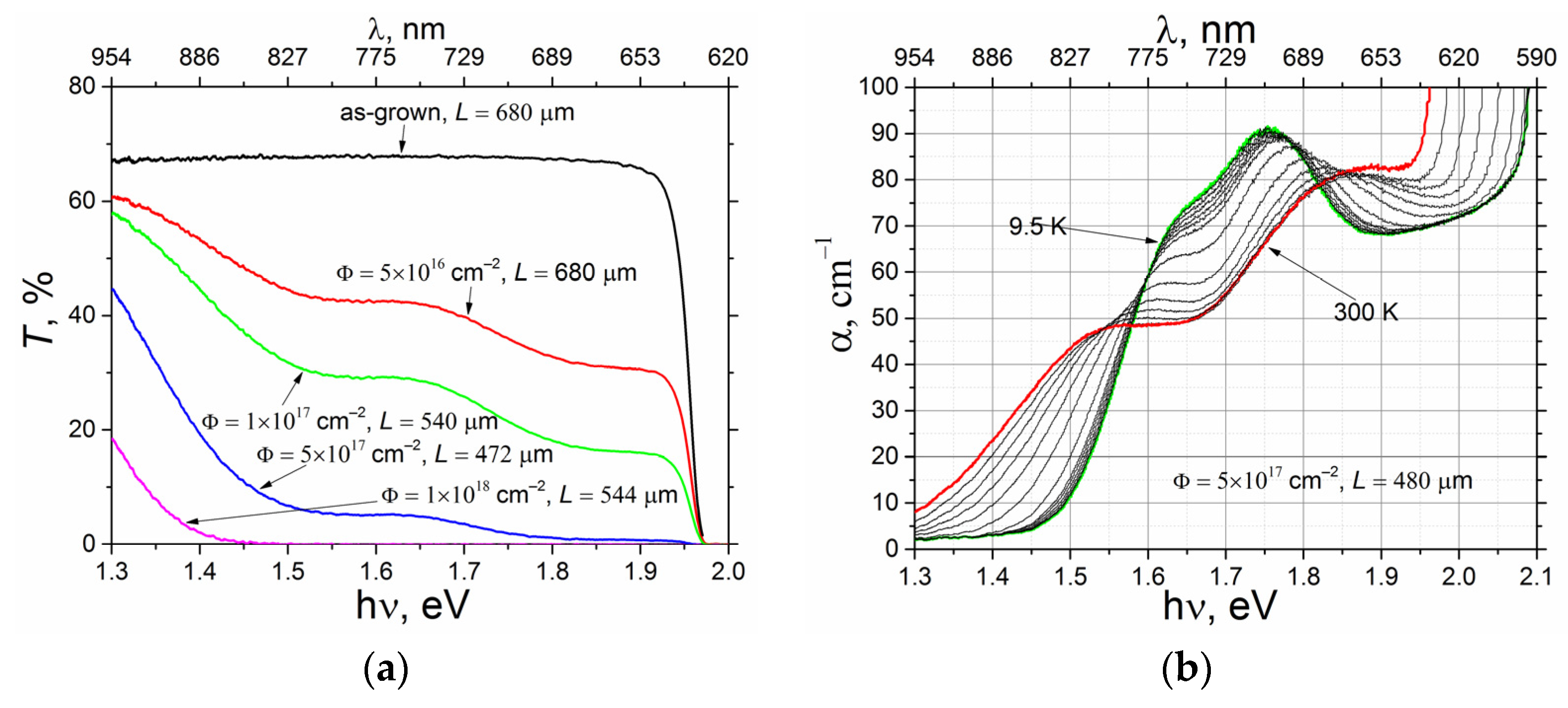
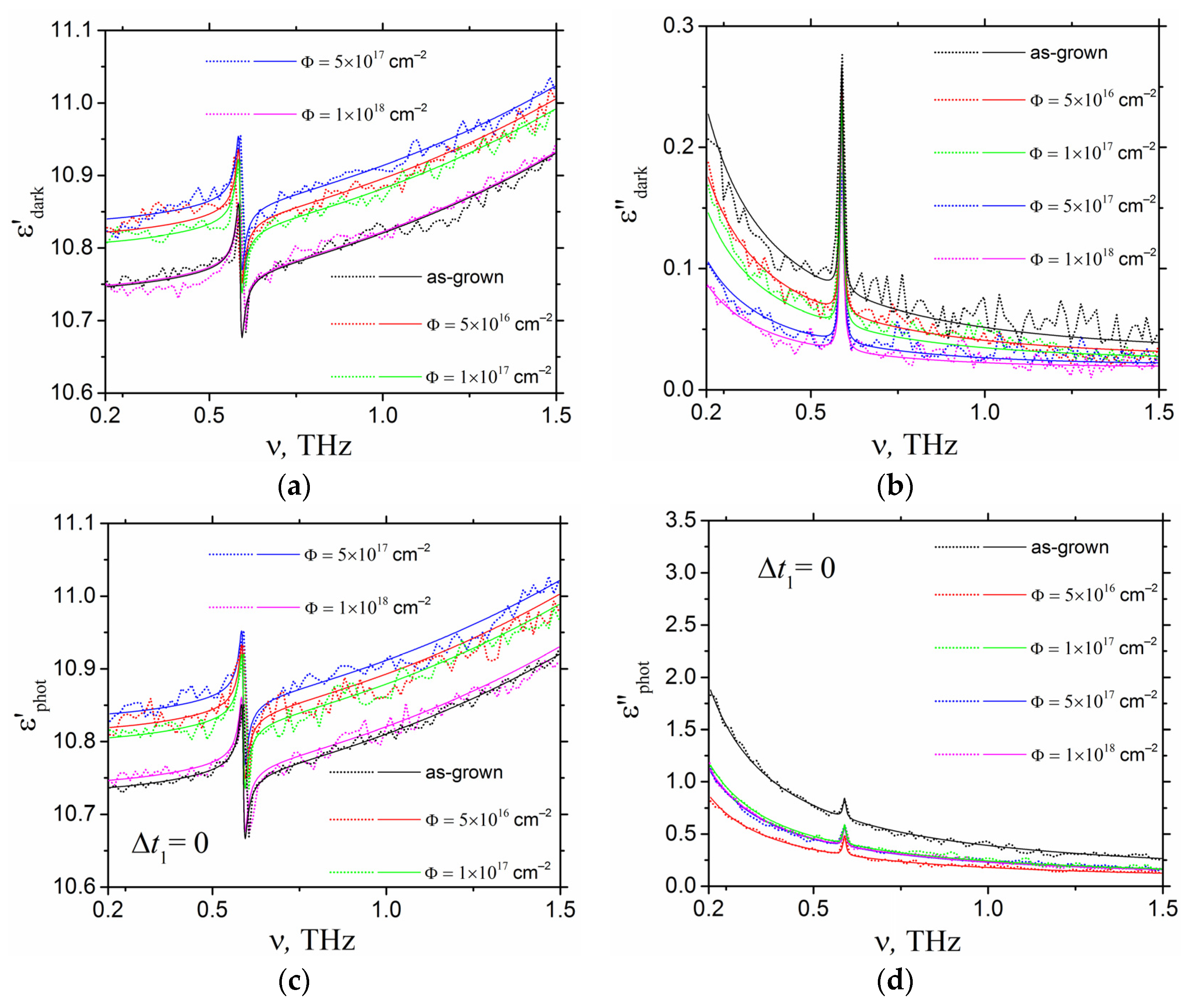
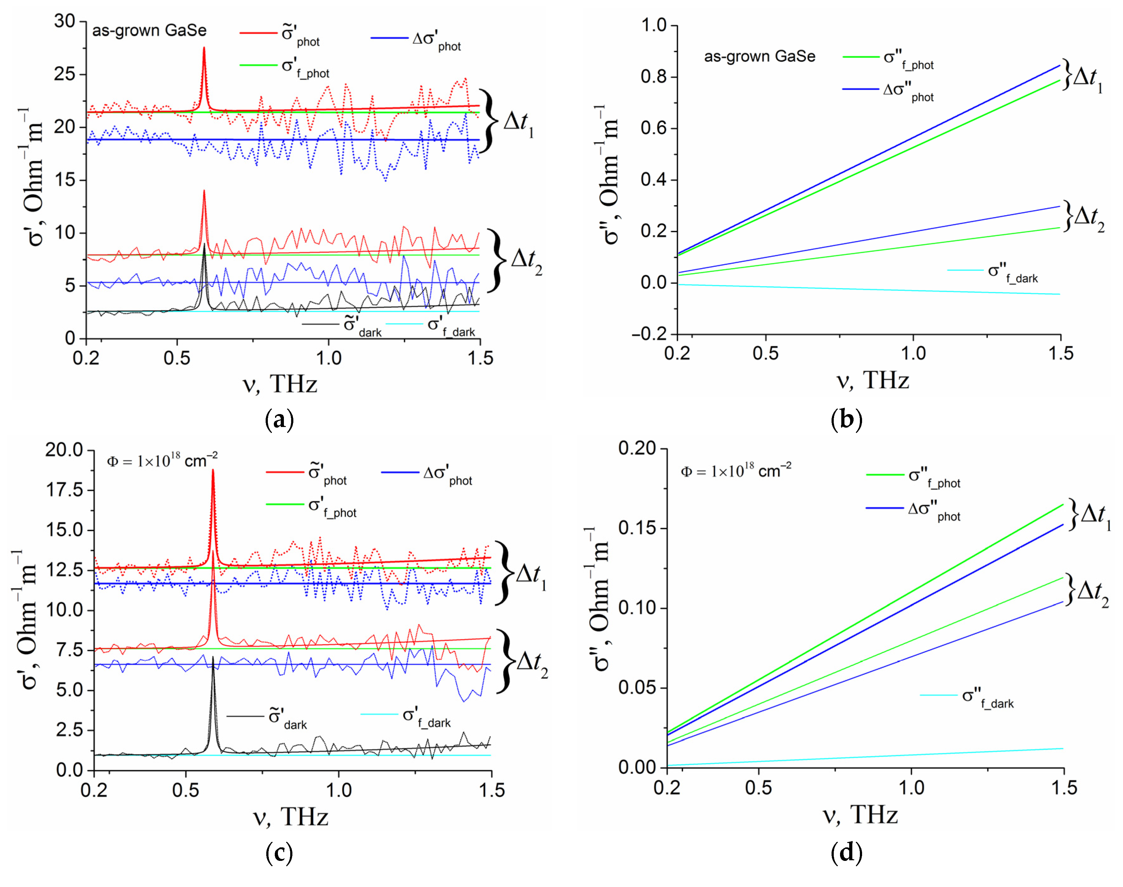
3. Results and Discussion

The obtained optical transmission spectra for the as-grown and electron-irradiated GaSe samples are shown in Figure 2a. Two absorption bands (looking like “steps”) are clearly seen on the transmission (Figure 2a) and absorption spectra (Figure 2b). The similar spectral features (“steps”) were previously observed in another representative of the III–VI class after neutron irradiation [24]. The absorption intensities for these two absorption bands definitely increase with increasing fluence (Figure 2a), while their spectral positions do not change. This testifies to the increase in the defect center concentration at increasing irradiation fluence, but not their type or charge state. On the absorption spectrum, calculated according to Equations (1) and (2), of the GaSe sample irradiated with Φ = 5 × 1017 cm−2 for various temperatures in the interval of 9.5–300 K, it can be seen that the lower-energy absorption band shifts toward lower photon energies at increasing temperature while its intensity decreases. The second (higher-energy) absorption band almost does not change its spectral position. Its absorption intensity looks higher at lower temperatures, but this can be an effect of the first absorption band, which overlaps with the second one at low temperatures. The fundamental absorption edge shift to higher photon energies at decreasing temperature is also clearly seen in Figure 2b. We performed fitting with Equation (4) of the absorption spectra of the electron-irradiated GaSe sample (Φ = 5 × 1017 cm−2), measured at temperatures of 9.5 and 300 K (Figure 2c). The obtained fitting parameters are given in Table 2. Contrary to the hydrogen model (employed also in [24] to describe the absorption “steps” in neutron irradiated GaS), in the employed model relation, the spectral position of the maximum absorption intensity does not match the photon energy of the supposed transition (EA) from the energy level in the forbidden band to the energy band but is located at ħω = 6·EA/5. It is seen that the model provides a satisfactory description of the observed spectral features (Figure 2c). The main discrepancy is between the experimental and the model curves in the spectral range of 1.8–2.09 eV for T = 9.5 K. The use of the dispersion relation no(λ) [37] in Equations (1) and (2) when calculating the absorption coefficients α(λ) from the measured transmission spectra T(λ) can be among the possible reasons. This dispersion relation is determined for room temperature and may deviate from a real dispersion of the refractive index at low temperatures, especially in the range above 1.8 eV, close to the room temperature band gap of GaSe. As can be seen from Table 2, the defect ionization energy for the lower-energy absorption band shifts to a lower photon energy at increasing temperature, while the absorption intensity of this band decreases. The defect ionization energy for the absorption band, observed at higher photon energies, almost does not change, while the absorption intensity increases on the contrary. Thus, the observable higher absorption intensity of the second “step” at the low temperature in Figure 2b is explained by the first absorption band contribution. Since there is absorption intensity “transfer” from the first (second) absorption band to the second (first) at increasing (decreasing) temperature (see Table 2), the involvement of a multiple charge defect could be supposed. We suppose that these could be the defect states induced by Ga vacancies in two charge states, having the energy positions at 0.23 and 0.61 eV above the valence band maximum (VBM) at T = 300 K (Figure 2d). This hypothesis is supported by the results of Refs. [30,45], where the acceptor state at 0.2 eV above the VBM was found in GaSe and attributed to the presence of Ga vacancies. Having the results of the fitting of the absorption spectra of the electron-irradiated GaSe sample (Φ = 5 × 1017 cm−2) (Figure 2c) and keeping in mind that the absorption coefficient provided by each of the two defect states equals ξ·N, where N is the concentration of the defect, we calculated the supposed concentrations of defects in each of the V Ga 1 and V Ga 2 charge states at T = 9.5 and 300 K (Table 2). The Gibbs distribution function was used (see the Supplementary Materials for details) [46]. According to the calculations, the concentrations of the defects in the two charge states (as specified in Table 2) at T = 300 K are provided at the Fermi-level position at (~0.2 kT below) the defect state at 0.61 eV above the VMB at a total defect concentration of about 7.3 × 1017 cm−3. The obtained value of the total VGa concentration is reasonable for Φ = 5 × 1017 cm−2. Analogously, the concentrations, specified in Table 2, of the defects at T = 9.5 K are provided at a Fermi-level position at (~1.8 kT above) the defect state at 0.57 eV above the VMB at a total defect concentration of about 7.5 × 1017 cm−3. Let us recall that the CNL position in GaSe, according to the calculations, is about 0.8 eV above the VBM [31]. The estimated position of the Fermi level for our experimental data is close to this energy position but not exactly the same.
The energy position of the V Ga 1 defect state rises together with the conduction band, while the energy position of the V Ga 2 state with respect to the VBM almost does not change (see Figure 2b–d and Table 2). Since the V Ga 2 induced states stay about 0.57 eV above the VBM, the photon energy required for the electron transition to the conduction band from these states increases when the temperature decreases.
It should be pointed out that the spectral shape of the observed spectra (Figure 2b,c) can be more accurately reproduced by fitting with Equation (5). The results of these fittings are provided in Figure S2a and Table S1 in the Supplementary Materials.
The proposed analysis (energy diagram) qualitatively explains the main observed spectral features and temperature dependencies of the absorption spectra of electron-irradiated GaSe crystals. Nevertheless, additional studies are required to more strictly determine the possible defects and processes responsible for the observed absorption bands. Intercenter transitions (to excited states of the defect in each charge state) as well as intercenter transitions between closely located defects (like divacancies) can also be involved.
As seen in Figure 3a, the observed radiation defects in GaSe are efficiently annealed. We performed the fitting of the integral absorption intensity for both observed bands (calculated according to Equation (6), the fitting parameters being obtained for the measured absorption curves after each annealing; see Figure S2b in the Supplementary Materials) using Equation (7) (Figure 2b). We considered the second-order recombination kinetics. We still point out that the same experimental data can be approximated with the equation for the first-order reaction. In real experimental conditions, both types of processes probably occur. Thus, the obtained values of the activation energies of defects are approximate. It is clearly seen that the activation energy is lower for the defect, responsible for the absorption band with EA1 = 1.35 eV, which starts to anneal at a temperature as low as 100 °C (Figure 3a). The absorption band with EA2 = 1.73 eV starts to anneal efficiently at about 300 °C. The shape of the spectra does not change during annealing, which, in turn, can be evidence of the absence of changes in related defect types (like changing distance between vacancies and interstitial atoms, which could give various energies for intercenter transitions). On the other hand, an existing influence of the defect charge state on its annealing efficiency has been reported [47]. Thus, there is a possibility that the VGa defects, having different charges, can be annealed at different temperatures (have different activation energies for annealing, as seen in Figure 3b).
The obtained experimental and model temporal profiles of the nonequilibrium charge carrier concentration for the as-grown and electron-irradiated GaSe samples are shown in Figure 4a. The fitting parameters (of Equation (14)) are provided in Table 3. It can be directly seen that the as-grown GaSe sample possesses a longer charge carrier lifetime compared to the irradiated samples. Thus, the irradiated samples probably contain more defects acting as efficient recombination centers. It is seen that the obtained b coefficient values increase with increasing fluence, which testifies to the increasing role of Auger recombination through defect states. It could be supposed that at electron irradiation, point defects are formed: first of all, Ga and Se vacancies, Se in the interlayer space and interstitial Ga atoms. According to the first-principles calculations, the Se and Ga vacancies can induce energy states close to the mid-gap (which usually act as efficient recombination centers) [48]. It is believed that electron irradiation produces, first of all, vacancies, while the interstitial atoms are easily annealed and clustered [28]. On the other hand, the DFT calculations [48] were performed for higher concentrations of defects (~5.7 × 1020 cm−3) than in our experiments (see Table 2), which is predicted by the limited size of the supercell. Thus, a defect-induced band is formed in the considered structure [48].
It can be mentioned that the method of decreasing the charge carrier lifetime would be needed to produce materials for dipole terahertz emitters. It is also possible that the irradiation with heavier particles or ion implantation [49] would produce more efficient recombination centers with shorter trapping times than observed for the electron irradiation. On the other hand, GaSe possesses a low charge carrier mobility (both static and at terahertz frequencies, as discussed below), and, thus, the dipole emitter would not be efficient compared to the GaAs-based structures [49].
The measured values of ΔT(t = 0)/T0 and the corresponding calculated values of μ (from Equation (12)) are also given in Table 3. In Figure 4b–d, the black curves represent the dependence τeffn) according to Equation (13) for the as-grown and GaSe samples irradiated with fluences of 5 × 10¹⁶ and 1 × 1018 cm−2, respectively. The red curves in Figure 4b–d represent the effective charge carrier lifetime if radiative and Auger recombination are absent (b = c = 0 in Equation (13)). The green and blue curves, in turn, describe the cases of dominant Auger recombination via traps (a = c = 0) and dominant interband Auger recombination (a = b = 0). The analogous plots for the rest of the samples are presented in the Supplementary Materials (Figure S3a,b).
The increase in coefficient b after the irradiation (while coefficient a decreases) may demonstrate that the Auger and SRH recombination pass through different defect states. Coefficient c also increases after the irradiation (Table 3).
The terahertz dielectric constant spectra measured in the dark and at Δt1 are presented in Figure 5. The fitting curves obtained using Equation (21) are also shown. The plots for Δt2 are provided in the Supplementary Materials (Figure S4a,b). The fitting parameters are given in Table 4. During fitting, the following fitting parameters, m* = 0.17 me, ωT1 = 3.7 THz, ωp1 = 212.2 GHz, γ1 = 65.7 GHz, ωT2 = 40.2 THz, ωp2 = 73 THz and γ2 = 367.5 GHz. were fixed for doped and photoexcited samples; only Drude–Smith parameters and the high-frequency dielectric constant were varied (the latter was kept the same for each sample irradiated with the same fluence). In Figure 5, the rigid-layer mode at 0.58 THz [37] is clearly seen. Its amplitude and shape are not affected by the photoexcitation or irradiation. The real part of the dielectric constant is almost the same for the samples irradiated with different fluences while the imaginary part gradually decreases at increasing irradiation fluence (Figure 5a,b). For the photoexcited samples, the comparison is not straightforward, as different photoexcitation conditions were applied (see Table 1). In general, the Lorentz–Drude–Smith model (Equation (21)) reproduces the experimental data well. The measured and calculated dark terahertz spectra of the absorption coefficient and the refractive index calculated using Equations (15) and (16) are given in the Supplementary Materials (Figure S5a,b).
In Figure 6, the experimental and calculated real and imaginary parts of the dark and photoexcited photoconductivity and free-carrier conductivity for the as-grown samples and those irradiated with fluence Φ = 1 × 1018 cm−2 are plotted. The corresponding real parts of total conductivity are also plotted in Figure 6a,c. The analogous plots for the rest of the samples are presented in the Supplementary Materials (Figures S6–S8). The imaginary parts of total conductivity are almost the same for the different samples and photoexcitation conditions (the example is provided in Figure S9 in the Supplementary Materials). It is seen that the contribution of the free-carrier conductivity (calculated with Equation (22) using parameters from Table 4) to the total conductivity of GaSe is dominant, except for the region about the phonon resonance. The difference between the total conductivity and the free-carrier conductivity still increases with increasing frequency. The dark conductivity decreases with increasing irradiation fluence. Both real and imaginary parts of the conductivity increase with increasing photoexcitation level. For the imaginary parts of the conductivities, only model curves are plotted in Figure 6b,d for a clear presentation (the difference between the curves is comparable to noise). The highest terahertz conductivity is observed in the as-grown GaSe. The terahertz conductivity decreases after electron irradiation. This follows the behavior of the static conductivity, as usually at high-energy particle irradiation (at not extremely high fluences), the Fermi level in semiconductors moves to the CNL and the conductivity reduces [28,50].
It was found that the terahertz charge carrier mobility in GaSe decreases after the electron irradiation. The low-frequency charge carrier mobility in GaSe also decreases at doping [6]. This is expectable, as both doping and electron irradiation induce defects. It should be noted that the charge carrier mobility values (Table 3) obtained from the measurements of the differential terahertz transmission after the photoexcitation are more reliable. This is because it is difficult to measure the low terahertz absorption with a high enough precision to determine the conductivity in high-resistivity samples.

4. Conclusions

In conclusion, optical absorption spectra of 9 MeV electron-irradiated GaSe crystals were studied. It was found that two absorption bands with the low-photon-energy threshold at 1.52 and 1.69 eV at T = 9.5 K and at 1.35 and 1.73 eV at T = 300 K appear in the transparency region of GaSe after the high-energy-electron irradiation. It was revealed that at changing temperatures the absorption intensities of these absorption bands possess inverse variation. To explain the observed experimental features, the observed absorption bands were attributed to the defect states induced by Ga vacancies in two charge states, having the energy positions at 0.23 and 0.61 eV above the valence band maximum at room temperature.
The OPTP technique was employed to study the dark and photoexcited terahertz conductivity and charge carrier recombination dynamics at two-photon excitation of as-grown and 9 MeV electron-irradiated GaSe crystals. The terahertz charge carrier mobilities were extracted from both the OPTP data and the Lorentz–Drude–Smith fitting of the dielectric constant spectra. The determined terahertz charge carrier mobility values were ~46 cm2/V·s and ~14 cm2/V·s for as-grown and heavily electron-irradiated GaSe crystals, respectively. The dependencies of the effective charge carrier lifetime on injection level were determined with decomposition into contributions from various recombination mechanisms. It was found that GaSe possesses a long charge carrier lifetime (a~1.9 × 10⁻⁶ ps−1, b~2.7 × 10⁻²¹ cm3ps−1 and c~1.3 × 10−37 cm6ps−1), i.e., τ~0.53 μs in the limit of a relatively low injection, when the contribution from SRH recombination is dominant. The electron irradiation of as-grown GaSe crystals reduced the charge carrier lifetime at a high injection level due to Auger recombination through radiation-induced defects. The terahertz spectra of dielectric constants of as-grown and electron-irradiated GaSe crystals were fitted using the Lorentz model, with the Drude–Smith term accounting for the free-carrier conductivity. It was found that the free-carrier conductivity makes the dominant contribution to the total terahertz conductivity in GaSe crystals.
The obtained results indicate the possibility of reducing the high-frequency conductivity and terahertz absorption of GaSe crystals through electron irradiation. This could be advantageous for the terahertz generation via difference frequency generation (DFG) or optical rectification with lasers having a wavelength > 1 μm, where the near-IR absorption produced by the irradiation-induced defects in GaSe is absent.

Supplementary Materials

The following supporting information can be downloaded at: https://www.mdpi.com/article/10.3390/cryst13111562/s1, Figure S1. Scheme of the experimental OPTP setup; Figure S2. Experimental and fitting (the fitting parameters for Equation (5) in the main text are given in Table S1) optical absorption spectra for the sample Φ = 5 × 1017 cm−2 measured at temperatures of 9.5 and 300 K (a); (b)—experimental and fitting (using Equation (4) in the main text) optical absorption spectra for the sample Φ = 5 × 1017 cm−2 measured at 300 K after isochronal (10 min) annealing at different temperatures; Figure S3. Calculated injection level dependences of efficient charge carrier lifetime with the resolution into contributions from different recombination mechanisms for (a) the GaSe sample irradiated with fluence of 1 × 1017 cm−2 and (b) the GaSe sample irradiated with fluence of 5 × 1017 cm−2. Figure S4. The terahertz spectra of real (a) and imaginary (b) parts of complex dielectric constant measured in as-grown and electron-irradiated GaSe crystals at time delay Δt2 after photoexcitation. Dotted lines—experimental data, solid lines–Lorentz–Drude–Smith fitting (the fitting parameters are given in Table 4 in the main text). Figure S5. The terahertz spectra of the absorption coefficient (a) and ordinary refractive index (b) measured in as-grown and electron-irradiated GaSe crystals (without photoexcitation). Figure S6. The terahertz spectra of real parts of the total conductivity, photoconductivity and free-carrier conductivity (a) and imaginary parts of photoconductivity and free-carrier conductivity (b) measured in the dark and at delays Δt1 and Δt2 after photoexcitation for the GaSe sample irradiated with fluence Φ = 5 × 1016 cm−2. Dotted lines—experimental data, solid lines—Lorentz–Drude–Smith fitting (the parameters are given in Table 4 in the main text). Figure S7. The terahertz spectra of real parts of the total conductivity, photoconductivity and free-carrier conductivity (a) and imaginary parts of photoconductivity and free-carrier conductivity (b) measured in the dark and at delays Δt1 and Δt2 after photoexcitation for the GaSe sample irradiated with fluence Φ = 1 × 1017 cm−2. Dotted lines —experimental data, solid lines—Lorentz–Drude–Smith fitting (the parameters are given in Table 4 in the main text). Figure S8. The terahertz spectra of real parts of the total conductivity, photoconductivity and free-carrier conductivity (a) and imaginary parts of photoconductivity and free-carrier conductivity (b) measured in the dark and at delays Δt1 and Δt2 after photoexcitation for the GaSe sample irradiated with fluence Φ = 5 × 1017 cm−2. Dotted lines —experimental data, solid lines—Lorentz–Drude–Smith fitting (the parameters are given in Table 4 in the main text). Figure S9. The model terahertz spectra of imaginary parts of dark total conductivity for the as-grown GaSe sample and total conductivity for the GaSe sample irradiated with fluence Φ = 5 × 1017 cm−2 for delay Δt2 after photoexcitation (the fitting parameters are given in Table 4 in the main text). The curves of the imaginary part of the total conductivity of the other samples and those measured at other photoexcitation conditions are not plotted because they are very close to the ones shown. Table S1. The fitting parameters of the optical absorption spectra, obtained by fitting with Equation (5) (in the main text), for the sample Φ = 5 × 1017 cm−2 measured at temperatures of 9.5 and 300 K.

Author Contributions

Conceptualization, V.N.B., Y.S.S. and S.Y.S.; methodology, R.A.R., S.A.B. and S.Y.S.; software, S.Y.S.; validation, V.N.B., X.S. and S.Y.S.; formal analysis, S.Y.S.; investigation, R.A.R., X.S. and S.Y.S.; resources, S.A.B. and V.N.B.; data curation, X.S. and S.Y.S.; writing—original draft preparation, S.Y.S.; writing—review and editing, X.S. and S.Y.S.; visualization, R.A.R.; supervision, S.Y.S.; project administration, S.Y.S.; funding acquisition, S.Y.S. All authors have read and agreed to the published version of the manuscript.

Funding

The part of the research focused on the study of the optical absorption spectra of electron-irradiated GaSe crystals was funded by the Ministry of Science and Higher Education of the Russian Federation (project No. FSWM-2020-0038). The part of the research focused on the study of GaSe terahertz properties was funded by a grant under the Decree of the Government of the Russian Federation No. 220 of 9 April 2010 (Agreement No. 075-15-2022-1132 of 1 July 2022). The authors also acknowledge the support from High-end Foreign Expert Introduction Program (G2023104003L).

Institutional Review Board Statement

Not applicable.

Informed Consent Statement

Not applicable.

Data Availability Statement

The data presented in this study are available in the article and Supplementary Materials.

Acknowledgments

The authors acknowledge the support from the Ministry of Science and Higher Education of the Russian Federation under project No. FSWM-2020-0038 and by a grant under the Decree of the Government of the Russian Federation No. 220 of 9 April 2010 (Agreement No. 075-15-2022-1132 of 1 July 2022). The authors acknowledge the assistance of Ilya A. Prudaev in the low-temperature absorption spectra measurements.

Conflicts of Interest

The authors declare no conflict of interest.

References

  1. Gouskov, A.; Gamassel, J.; Gouskov, L. Growth and characterization of III–V layered crystals like GaSe, GaTe, InSe, GaSe1-xTex and GaxIn1-xSe. Prog. Cryst. Growth Charact. Mater. 1982, 5, 323–413. [Google Scholar] [CrossRef]
  2. Sarkisov, S.Y.; Kosobutsky, A.V.; Shandakov, S.D. Effect of van der Waals interactions on the structural and binding properties of GaSe. J. Solid State Chem. 2015, 232, 67–72. [Google Scholar] [CrossRef]
  3. Arora, H.; Erbe, A. Recent progress in contact, mobility, and encapsulation engineering of InSe and GaSe. InfoMat 2021, 3, 662–693. [Google Scholar] [CrossRef]
  4. Redkin, R.A.; Kobtsev, D.A.; Kolesnikova, I.A.; Bereznaya, S.A.; Sarkisov, Y.S.; Voevodin, V.I.; Mihaylov, T.A.; Novikov, V.A.; Sarkisov, S.Y. The visibility and stability of GaSe nanoflakes of about 50 layers on SiO2/Si wafers. Int. J. Mod. Phys. B 2021, 35, 2150273. [Google Scholar] [CrossRef]
  5. Palmer, J.E.; Saitoh, T.; Yodo, T.; Tamura, M. Growth and characterization of GaAs/GaSe/Si heterostructures. Jpn. J. Appl. Phys. 1993, 32, L1126. [Google Scholar] [CrossRef]
  6. Atuchin, V.V.; Bereznaya, S.A.; Beisel, N.F.; Korotchenko, Z.V.; Kruchinin, V.N.; Pokrovsky, L.D.; Saprykin, A.I.; Sarkisov, S.Y. Growth, chromium distribution and electrical properties of GaSe:Cr single crystals. Mat. Chem. Phys. 2014, 146, 12–17. [Google Scholar] [CrossRef]
  7. Voevodin, V.G.; Voevodina, O.V.; Bereznaya, S.A.; Korotchenko, Z.V.; Morozov, A.N.; Sarkisov, S.Y.; Fernelius, N.C.; Goldstein, J.T. Large single crystals of gallium selenide: Growing, doping by in and characterization. Opt. Mater. 2004, 26, 495–499. [Google Scholar] [CrossRef]
  8. Zhou, Y.; Nie, Y.; Liu, Y.; Yan, K.; Hong, J.; Jin, C.; Zhou, Y.; Yin, J.; Liu, Z.; Peng, H. Epitaxy and photoresponse of two-dimensional GaSe crystals on flexible transparent mica sheets. ACS Nano 2014, 8, 1485–1490. [Google Scholar] [CrossRef] [PubMed]
  9. Zhao, Y.-F.; Fuh, H.-R.; Coileáin, C.Ó.; Cullen, C.P.; Stimpel-Lindner, T.; Duesberg, G.S.; Leonardo Camargo, Ó.; Zhang, D.; Cho, J.; Choi, M.; et al. Highly sensitive, selective, stable, and flexible NO2 sensor based on GaSe. Adv. Mater. Technol. 2020, 5, 1901085. [Google Scholar] [CrossRef]
  10. Schubert, O.; Hohenleutner, M.; Langer, F.; Urbanek, B.; Lange, C.; Huttner, U.; Golde, D.; Meier, T.; Kira, M.; Koch, S.W.; et al. Sub-cycle control of terahertz high-harmonic generation by dynamical Bloch oscillations. Nat. Photonics 2014, 8, 119–123. [Google Scholar] [CrossRef]
  11. Huber, R.; Brodschelm, A.; Tauser, F.; Leitenstorfer, A. Generation and field-resolved detection of femtosecond electromagnetic pulses tunable up to 41 THz. Appl. Phys. Lett. 2000, 76, 3191–3193. [Google Scholar] [CrossRef]
  12. Junginger, F.; Sell, A.; Schubert, O.; Mayer, B.; Brida, D.; Marangoni, M.; Cerullo, G.; Leitenstorfer, A.; Huber, R. Single-cycle multiterahertz transients with peak fields above 10 MV/cm. Opt. Lett. 2010, 35, 2645–2647. [Google Scholar] [CrossRef] [PubMed]
  13. Knorr, M.; Raab, J.; Tauer, M.; Merkl, P.; Peller, D.; Wittmann, E.; Riedle, E.; Lange, C.; Huber, R. Phase-locked multi-terahertz electric fields exceeding 13 MV/cm at a 190 kHz repetition rate. Opt. Lett. 2017, 42, 4367–4370. [Google Scholar] [CrossRef] [PubMed]
  14. Sell, A.; Leitenstorfer, A.; Huber, R. Phase-locked generation and field-resolved detection of widely tunable terahertz pulses with amplitudes exceeding 100 MV/cm. Opt. Lett. 2008, 33, 2767–2769. [Google Scholar] [CrossRef] [PubMed]
  15. Liu, K.; Xu, J.; Zhang, X.-C. GaSe crystals for broadband terahertz wave detection. Appl. Phys. Lett. 2004, 85, 863–865. [Google Scholar] [CrossRef]
  16. Keilmann, F.; Amarie, S. Mid-infrared frequency comb spanning an octave based on an Er fiber laser and difference-frequency generation. J. Infrared Millim. Terahertz Waves 2012, 33, 479–484. [Google Scholar] [CrossRef]
  17. Su, X.; Lyu, M.; Hoang, T.; Xu, Z.; Zheng, Y.; Strickland, D. Investigation of long wavelength mid-infrared generation in the tight focusing limit. Opt. Express 2019, 27, 24945–24952. [Google Scholar] [CrossRef] [PubMed]
  18. Su, X.; Zhu, R.; Wang, B.; Bai, Y.; Ding, T.; Sun, T.; Lü, X.; Peng, J.; Zheng, Y. Generation of 8–20 μm mid-infrared ultrashort femtosecond laser pulses via difference frequency generation. Photonics 2022, 9, 372. [Google Scholar] [CrossRef]
  19. Cao, Q.; Kärtner, F.X.; Chang, G. Towards high power longwave mid-IR frequency combs: Power scalability of high repetition-rate difference-frequency generation. Opt. Express 2020, 28, 1369–1384. [Google Scholar] [CrossRef]
  20. Liu, Y.; Zhao, J.; Wei, Z.; Kärtner, F.X.; Chang, G. High-power, high-repetition-rate tunable longwave mid-IR sources based on DFG in the OPA regime. Opt. Lett. 2023, 48, 1052–1055. [Google Scholar] [CrossRef]
  21. Beechem, T.E.; Kowalski, B.M.; Brumbach, M.T.; McDonald, A.E.; Spataru, C.D.; Howell, S.W.; Ohta, T.; Pask, J.A.; Kalugin, N.G. Oxidation of ultrathin GaSe. Appl. Phys. Lett. 2015, 107, 173103. [Google Scholar] [CrossRef]
  22. Redkin, R.A.; Kobtsev, D.A.; Bereznaya, S.A.; Korotchenko, Z.V.; Sarkisov, Y.S.; Mihaylov, T.A.; Sarkisov, S.Y. GaSe crystals with antireflection coatings for terahertz generation. Mater. Res. Express 2019, 6, 126201. [Google Scholar] [CrossRef]
  23. Hagner, M.; Sulzer, P.; Liehl, A.; Cimander, M.; Kempf, H.; Bitzer, A.; Herter, A.; Leitenstorfer, A. Ultrabroadband suppression of mid-infrared reflection losses of a layered semiconductor by nanopatterning with a focused ion beam. Opt. Express 2021, 29, 33632–33641. [Google Scholar] [CrossRef] [PubMed]
  24. Manjon, F.J.; Segura, A.; Munoz, V. Neutron irradiation defects in gallium sulfide: Optical absorption measurements. J. Appl. Phys. 1997, 81, 6651–6656. [Google Scholar] [CrossRef]
  25. Pareja, R.; De la Cruz, R.M.; Mari, B.; Segura, A.; Muñoz, V. Thermal recovery of the lattice damage in neutron-transmutation-doped InSe. Phys. Rev. B 1993, 47, 2870–2873. [Google Scholar] [CrossRef] [PubMed]
  26. Mari, B.; Segura, A.; Chevy, A. Electrical properties of neutron-transmutation-doped InSe. Appl. Surf. Sci. 1991, 50, 415–419. [Google Scholar] [CrossRef]
  27. Nakatani, H.; Sakai, E.; Tatsuyama, C.; Takeda, F. GaSe nuclear particle detectors. Nucl. Instrum. Methods Phys. Res. A 1989, 283, 1361–1365. [Google Scholar] [CrossRef]
  28. Brudnyi, V.N.; Budnitskii, D.L.; Krivov, M.A.; Masagutova, R.V.; Prochukhan, V.D.; Rud, Y.V. The electrical and optical properties of 2.0 MeV electron-irradiated ZnGeP2. Phys. Status Solidi 1978, 50, 379–384. [Google Scholar] [CrossRef]
  29. Voevodin, V.I.; Bereznaya, S.A.; Sarkisov, Y.S.; Yudin, N.N.; Sarkisov, S.Y. Terahertz generation by optical rectification of 780 nm laser pulses in pure and Sc-doped ZnGeP2 crystals. Photonics 2022, 9, 863. [Google Scholar] [CrossRef]
  30. Micocci, G.; Siciliano, P.; Tepore, A. Deep level spectroscopy in pGaSe single crystals. J. Appl. Phys. 1990, 10, 6582. [Google Scholar]
  31. Brudnyi, V.N.; Sarkisov, S.Y.; Kosobutsky, A.V. Electronic properties of GaSe, InSe, GaS and GaTe layered semiconductors: Charge neutrality level and interface barrier heights. Semicond. Sci. Technol. 2015, 30, 115019. [Google Scholar] [CrossRef]
  32. Micocci, G.; Serra, A.; Tepore, A. Impurity levels in Sn-doped GaSe semiconductor. Phys. Stat. Sol. 1997, 162, 649–659. [Google Scholar] [CrossRef]
  33. Minder, R.; Ottaviani, G.; Canali, C. Charge transport in layer semiconductors. J. Phys. Chem. Solids 1976, 37, 417–424. [Google Scholar] [CrossRef]
  34. Wahlstrand, J.K.; Heilweil, E.J. Contactless THz-based bulk semiconductor mobility measurements using two-photon excitation. Opt. Express 2018, 26, 29848–29853. [Google Scholar] [CrossRef] [PubMed]
  35. Jepsen, P.U.; Cooke, D.G.; Koch, M. Terahertz spectroscopy and imaging—Modern techniques and applications. Las. Phot. Rev. 2011, 5, 124–166. [Google Scholar] [CrossRef]
  36. Voevodin, V.I.; Brudnyi, V.N.; Sarkisov, Y.S.; Su, X.; Sarkisov, S.Y. Electrical relaxation and transport properties of ZnGeP2 and 4H-SiC crystals measured with terahertz spectroscopy. Photonics 2023, 10, 827. [Google Scholar] [CrossRef]
  37. Chen, C.-W.; Tang, T.-T.; Lin, S.-H.; Huang, J.Y.; Chang, C.-S.; Chung, P.-K.; Yen, S.-T.; Pan, C.-L. Optical properties and potential applications of ε-GaSe at terahertz frequencies. J. Opt. Soc. Am. B 2009, 26, A58–A65. [Google Scholar] [CrossRef]
  38. Lucovsky, G. On the photoionization of deep impurity centers in semiconductors. Solid State Commun. 1965, 3, 299–302. [Google Scholar] [CrossRef]
  39. Fleurov, V.N.; Kikoin, K.A. k.p perturbation theory for light absorption in semiconductors doped by 3D metals. J. Phys. C Solid State Phys. 1982, 15, 3523–3537. [Google Scholar] [CrossRef]
  40. Lucovsky, G. Optical absorption associated with deep impurity centers in semiconductors. Bull. Am. Phys. Soc. 1966, 11, 206. [Google Scholar]
  41. Zotova, I.B.; Ding, Y.J. Spectral measurements of two-photon absorption coefficients for CdSe and GaSe crystals. Appl. Opt. 2001, 40, 6654–6658. [Google Scholar] [CrossRef] [PubMed]
  42. Kolesnikova, I.A.; Kobtsev, D.A.; Redkin, R.A.; Voevodin, V.I.; Tyazhev, A.V.; Tolbanov, O.P.; Sarkisov, Y.S.; Sarkisov, S.Y.; Atuchin, V.V. Optical pump—THz probe study of HR GaAs:Cr and SI GaAs:EL2 structures with long charge carrier lifetimes. Photonics 2021, 8, 575. [Google Scholar] [CrossRef]
  43. Shi, Y.; Zhou, Q.; Zhang, C.; Jin, B. Ultrafast high-field carrier transport in GaAs measured by femtosecond pump-probe terahertz spectroscopy. Appl. Phys. Lett. 2008, 93, 121115. [Google Scholar] [CrossRef]
  44. Ottaviani, G.; Canali, C.; Nava, F.; Schmid, P.; Mooser, E.; Minder, R.; Zschokke, I. GaSe: A layer compound with anomalous valence band anisotropy. Solid State Commun. 1974, 14, 933–936. [Google Scholar] [CrossRef]
  45. Shigetomi, S.; Ikari, T. Optical and electrical characteristics of p-GaSe doped with Te. J. Appl. Phys. 2004, 95, 6480–6482. [Google Scholar] [CrossRef]
  46. Bonch-Bruevich, V.L.; Kalashnikov, S.G. Physics of Semiconductors; VEB Deutscher Verlag der Wissenschaften: Berlin, Germany, 1982. (In German) [Google Scholar]
  47. Mamontov, A.P.; Peshev, V.V.; Chernov, I.P. Role of charged state in build-up and annealing of deep centers in GaAs irradiated by protons. USSR Rept. Electron. Elec. Eng. JPRS UEE 1984, 17, 23. [Google Scholar]
  48. Rak, Z.; Mahanti, S.D.; Mandal, K.C.; Fernelius, N.C. Electronic structure of substitutional defects and vacancies in GaSe. J. Phys. Chem. Solids 2009, 70, 344–355. [Google Scholar] [CrossRef]
  49. Brudnyi, V.N.; Potapov, A.I. Electrical properties of the proton-irradiated semi-insulating GaAs: Cr. Semiconductors 2001, 35, 1361–1365. [Google Scholar] [CrossRef]
  50. Singh, A.; Pal, S.; Surdi, H.; Prabhu, S.S.; Mathimalar, S.; Nanal, V.; Pillay, R.G.; Dohler, G.H. Carbon irradiated semi insulating GaAs for photoconductive terahertz pulse detection. Opt. Express 2015, 23, 6656–6661. [Google Scholar] [CrossRef]
Figure 1. Calculated dependences of the e-h pair concentration averaged over the length of a crystal and of the concentration of photogenerated e-h pairs on distance x from the illuminated surface of a crystal for the measurements of the terahertz photoconductivity and the charge carrier relaxation dynamics in as-grown and electron-irradiated GaSe crystals.
Crystals 13 01562 g001
Figure 2. (a)—Room temperature transparency spectra of the as-grown and electron-irradiated GaSe crystals; (b)—optical absorption spectra for the sample irradiated with Φ = 5 × 1017 cm−2 measured at temperatures of 9.5 K, 15–40 K with a step of 5 K and 60–300 K with a step of 40 K; (c)—experimental and fitting (the parameters are given in Table 2) optical absorption spectra for the sample Φ = 5 × 1017 cm−2 measured at temperatures of 9.5 and 300 K; (d) supposed energy diagram with the related optical transitions and energy positions of the defect states and the Fermi level for electron-irradiated GaSe sample at temperatures of 9.5 and 300 K. The thicknesses of the samples and the irradiation fluences are shown on the plots.
Crystals 13 01562 g002aCrystals 13 01562 g002b
Figure 3. (a)—Room temperature transparency spectra of GaSe sample after 9 MeV electron irradiation with fluence Φ = 5 × 1017 cm−2 and after its subsequent annealing for 10 min at a temperature of 100, 200, 300 and 400 °C; (b)—experimental and fitting absorption intensity dependence (for each of the two bands, see Table 2) on annealing temperature for the GaSe sample irradiated with fluence Φ = 5 × 1017 cm−2 (fitting parameters of Equation (7) are shown on the plot).
Crystals 13 01562 g003
Figure 4. (a)—Experimental and fitting (the parameters are given in Table 3) time dependences of the nonequilibrium charge carrier concentration in the as-grown and electron-irradiated GaSe crystals; (bd)—related calculated injection level dependences of the efficient charge carrier lifetime with the resolution into contributions from the different recombination mechanisms for the as-grown and GaSe samples irradiated with fluences of 5 × 10¹⁶ and 1 × 1018 cm−2.
Crystals 13 01562 g004
Figure 5. The terahertz spectra of real (a,c) and imaginary (b,d) parts of complex dielectric constant measured in as-grown and electron-irradiated GaSe crystals in the dark (a,b) and at time delay Δt1 after photoexcitation (c,d). Dotted lines—experimental data, solid lines—Lorentz–Drude–Smith fitting (the fitting parameters are given in Table 4).
Crystals 13 01562 g005
Figure 6. The terahertz spectra of real parts of the total conductivity, photoconductivity and free-carrier conductivity (a,c) and imaginary parts of photoconductivity and free-carrier conductivity (b,d) measured in the dark and at delays Δt1 and Δt2 after photoexcitation for the as-grown GaSe and that irradiated with fluence Φ = 1 × 1018 cm−2. Dotted lines—experimental data, solid lines—Lorentz–Drude–Smith fitting (the parameters are given in Table 4).
Crystals 13 01562 g006
Table 1. Experimental sample and photoexcitation parameters.
Sampleα (λ = 800 nm),
cm−1
L, μmPav, mWd, mmΔn,
cm−3
Δne-h_pairs, cm−3
Front
Surface
Outflow
Surface
as-grown0.0110018043.31 × 10163.89 × 10162.81 × 1016
Φ = 5 × 1016 cm−25.1140023052.1 × 10163.52 × 10161.25 × 1016
Φ = 1 × 1017 cm−213.0913023053.9 × 10165 × 10163.05 × 1016
Φ = 5 × 1017 cm−250.8813023065.11 × 10167.65 × 10163.3 × 1016
Φ = 1 × 1018 cm−2155.8113015065.51 × 10161.33 × 10171.64 × 1016
Table 2. The fitting parameters obtained by fitting with Equation (4) of the optical absorption spectra for the sample Φ = 5 × 1017 cm−2 measured at temperatures of 9.5 and 300 K and the estimated concentrations of defects in each of the V Ga 1 and V Ga 2 charge states.
Parameter9.5 K300 K
A1, cm−1eV5/2930 (N = 6.4 × 1017 cm−3)400 (N = 3.3 × 1017 cm−3)
EA1, eV1.521.35464
A2, cm−1eV5/2180 (N = 1.1 × 1017 cm−3)690 (N = 4 × 1017 cm−3)
EA2, eV1.691.72833
A3, cm−1eV−1/219471947
Eg, eV2.091.96
Table 3. The data of OPTP measurements and related values of charge carrier motility and a, b and c fitting parameters.
SampleL,
μm
−ΔT (t = 0)/T0Δn (t = 0),
cm−3
μ,
cm2/V × s
a,
ps−1
b,
ps−1 cm3
c,
ps−1 cm6
as-grown1000.143.31 × 1016461.9 × 10−62.7 × 10−211.3 × 10−37
Φ = 5 × 1016 cm−24000.162.1 × 1016207 × 10−73.2 × 10−212.6 × 10−36
Φ = 1 × 1017 cm−21300.083.9 × 1016163.6 × 10−73.4 × 10−218 × 10−36
Φ = 5 × 1017 cm−21300.095.11 × 1016153.7 × 10−73.6 × 10−211.8 × 10−36
Φ = 1 × 1018 cm−21300.095.51 × 1016143.6 × 10−74.4 × 10−214.1 × 10−36
Table 4. The Lorentz–Drude–Smith model fitting parameters (m* = 0.17 me, ωT1 = 3.7 THz, ωp1 = 212.2 GHz, γ1 = 65.7 GHz, ωT2 = 40.2 THz, ωp2 = 73 THz, γ2 = 367.5 GHz).
SampleL,
μm
Photoexcitation Delayμ,
cm2/V·s
εn, cm−3τ,
fs
cb
as-grown100dark477.448.32 × 10154.5−0.58
Δt2307.441.66 × 10162.9−1.2 × 10⁻⁴
Δt1407.443.31 × 10163.90
Φ = 5 × 1016 cm−2400dark217.527 × 10152−0.12
Δt2327.521.05 × 10163.10
Δt1297.522.1 × 10162.80
Φ = 1 × 1017 cm−2130dark177.56.2 × 10151.60
Δt2227.51.95 × 10162.10
Δt1217.53.9 × 101620
Φ = 5 × 1017 cm−2130dark167.535.32 × 10151.5−0.07
Δt2157.532.55 × 10161.40
Δt1167.535.11 × 10161.50
Φ = 1 × 1018 cm−2130dark157.444.32 × 10151.40
Δt2187.442.76 × 10161.70
Δt1157.445.51 × 10161.40
Disclaimer/Publisher’s Note: The statements, opinions and data contained in all publications are solely those of the individual author(s) and contributor(s) and not of MDPI and/or the editor(s). MDPI and/or the editor(s) disclaim responsibility for any injury to people or property resulting from any ideas, methods, instructions or products referred to in the content.

