Abstract
Luminophores featuring thermally activated delayed fluorescence (TADF) are the workhorses of the third- and fourth-generation OLEDs. While these compounds have usually been used as dopants embedded in the host, non-doped TADF OLEDs have recently shown significant progress as well and have attained performances comparable to those of the host-dopant systems. For efficient operation of non-doped OLEDs, the charge transport in neat films and single crystals of TADF luminophores is important; however, this issue was nearly unexplored theoretically. In the current study, we calculated the charge-carrier mobilities in four single crystals of TADF luminophores that have different molecular packing motifs. Specifically, in one of them both the donor and acceptor moieties form uniform π-stacks, while in the others the donors (acceptors) show alternating lateral shifts along the stacks; the difference in the molecular packing resulted in the difference in the transfer integrals between the molecules. The reorganization energies differed as well by up to four times for the studied crystals. As a result, the charge mobilities varied from 0.001 to ~0.3 cm2/(V∙s), with the largest being predicted for the crystal of the luminophore that consisted of a rigid donor and acceptor. We anticipate that the results obtained will be useful in the design of TADF luminophores for non-doped OLEDs, OLETs, and other organic light-emitting devices.
1. Introduction
Organic light-emitting diodes (OLEDs) are leaders in commercialization among organic electronic devices. Their wide application in displays and lighting panels is based on their high luminance and contrast, flexibility, true black color, relatively inexpensive production, small weight (no metal and no quartz substrate), and size [1,2,3,4]. The first generation of OLEDs utilized fluorophores and had a small external quantum efficiency (EQE) because 75% of the electrically generated excitons were lost in non-emissive triplet states. On the contrary, second-generation OLEDs exploited phosphorescent luminophores in which triplet excitons were harvested, but these devices suffered from poor color purity and smaller luminance. Finally, third- and fourth-generation OLEDs are based on luminophores that exhibit thermally activated delayed fluorescence (TADF). In these compounds, the lowest triplet states are close in energy to the lowest singlet excited states. This allows thermal fluctuations to perform reverse intersystem crossing to repopulate the singlet state from the triplet one and enable delayed fluorescence [5].
TADF luminophores typically consist of donor and acceptor moieties [5]. Accordingly, the frontier molecular orbitals of these luminophores are separated: the highest occupied molecular orbital (HOMO) is located mainly on the donor moiety (or moieties), while the lowest unoccupied molecular orbital (LUMO) is located mainly on the acceptor moiety (or moieties). Moreover, the donor and acceptor moieties are usually orthogonal due to steric hindrance that prevents their coplanar orientation. All this weakens the overlapping between the HOMO and LUMO and hence decreases the energy difference between the lowest excited singlet and lowest triplet states, which is necessary for efficient TADF. Although TADF luminophores have highly non-planar and asymmetrical structures, they frequently form single crystals; molecular packing for several of them was recently reported (see, e.g., Refs. [6,7,8,9,10]). However, a detailed analysis of the crystal structures and the intermolecular interaction in them is lacking.
Usually, TADF luminophores are used as dopants that are embedded in the amorphous organic semiconducting host. However, non-doped TADF OLEDs in which pristine films of TADF luminophores serve as light-emitting layers recently gained attention due to their ease of manufacturing and better operational stability and reproducibility [5,11]. Remarkably, the reported EQE values for the non-doped TADF OLEDs were lower but already comparable to those of the conventional (host-dopant) ones [5,11,12,13]. In non-doped OLEDs, the luminophore film needs to maintain the transport of holes and electrons, which is in contrast to the conventional OLEDs where this function is delivered to the host. The experimental charge-carrier (electron and/or hole) mobilities in thin films of TADF luminophores were reported in several studies. Generally, these values were in the range of 10−8–10−4 cm2/(V∙s) [14,15,16,17], which is a characteristic order for polycrystalline or amorphous films of organic semiconductors [18]. However, the intrinsic (i.e., in the case of the absence of defects and contact issues) charge mobility for single crystals of these luminophores could be much larger and reach that observed for standard single-crystalline organic semiconductors (far above 1 cm2/(V∙s)) [18,19], including those used as active layers in organic light-emitting transistors (OLETs or LEFETs) [20,21]. This anticipation was corroborated by the fact that OFET measurements for some host-dopant blends of TADF luminophores showed charge mobilities of up to ~0.2 cm2/(V∙s) [22] and 0.8 cm2/(V∙s) [23]. Hence, the search for TADF luminophores with efficient charge transport is important for the improvement of non-doped TADF OLEDs.
Since the reliable estimation of the intrinsic charge mobility is a very delicate and time-consuming task [24], the theoretical prediction of electron and hole mobilities is important for the design of luminophores for non-doped OLEDs. It is natural to start such investigation from the crystal structures obtained from X-ray data because the latter can shed light on the molecular packing that is typical for the compounds studied. However, theoretical studies of the charge transport in crystals or amorphous films of TADF luminophores are extremely rare: we are aware of only one such investigation [14]. Thus, a comparative theoretical study of the charge transport in various TADF crystals is important to reveal the structure–property relationships and formulate guidelines for the design of TADF luminophores for non-doped OLEDs.
In this work, we compared the crystal structures of four TADF luminophores: oTE-DRZ, CPPD, PXZ-XO, and TRZ-c-BPXZ, the X-ray data for which were reported earlier. The Hirshfeld analysis and energy-framework approaches were applied to unveil the differences in the crystal packing. In the first crystal, columnar packing of the molecules was observed in which the donor and acceptor moieties formed segregated π-stacks, which provided overlap of the HOMOs (LUMOs). In the three remaining crystals, the donor and acceptor moieties were also segregated, but their packing in the stacks was non-homogeneous: they formed tightly interacting dimers that interacted weakly with their neighbors. We calculated the transfer integrals and reorganization energies for the compounds studied and then estimated the hole and electron mobilities therein within the hopping model, which is frequently used to estimate the charge mobility in organic semiconductors [25,26,27]. The relationship between the charge mobilities and molecular/crystal structure was discussed, which could facilitate the rational design of TADF luminophores for non-doped OLEDs and other light-emitting organic devices.
2. Methods
2.1. Crystal Structure Analysis
The Hirshfeld surface analysis and energy-framework calculations were performed in CrystalExplorer software (version 21.5) [28] at the B3LYP-D2/6-31g(d,p) level. Note that according to Ref. [29], using the D2 dispersion correction scheme in CrystalExplorer is preferable to using D3. For the energy-framework calculations, a molecular shell with a 3.8 Å radius was generated around a central molecule, and the interaction energies (electrostatic, dispersion, and total) between the molecular pairs were calculated. The scale factors for the benchmarked energies used for the construction of the energy models were taken from Ref. [30]. The crystal structures were obtained from the CCDC database: 1905959 [6], 1922220 [7], and 2043193 [9] for oTE-DRZ, CPPD, and TRZ-c-BPXZ, respectively. The crystal data for PXZ-XO were obtained from Ref. [8]. No further geometry optimization was performed.
2.2. Charge Mobility
To estimate the charge mobility within the hopping model, the charge transfer rates from a given molecule A to each of its nearest neighbors (e.g., molecule B) were calculated using the Marcus formula [31]:
where J is the transfer integral describing the electronic interaction between the two molecules, λ is the reorganization energy describing the strength of the electron–phonon coupling, ħ is the reduced Planck constant, k is the Boltzmann constant, T is the absolute temperature, and ΔE is the electron energy difference between the initial and final sites (ΔE = 0 if the molecules are similar). The protocol for the J and λ calculation is described below. In the case of molecular “dimerization” along some direction, when the molecule A formed a tightly interacting dimer with a molecule B that possessed a large JAB but the latter molecule interacted weakly with the next molecule C in this direction via a small JBC, we described the effective transfer rate along this direction as . This expression stemmed from the fact that the transition time from A to C (tAC = 1/kAC) was composed of tAB = 1/kAB and tBC = 1/kBC. Finally, the charge mobility was calculated using the Einstein–Smoluchowski relation:
where D is the charge carrier (polaron) diffusion coefficient, ri is the distance between the adjacent molecules along the i-th transport direction (dimers in the case of dimerization), and is the probability of the charge carrier to move in this direction.
As follows from Equation (1), the main parameters of the hopping model are transfer integrals (J) and reorganization energies (λ). The former were calculated using home-written code based on the dimer projection method (DIPRO) [32,33,34]. To estimate this quantity for a pair (dimer) of molecules (monomers) A and B, the wavefunctions of these molecules were approximated by their HOMOs (for hole transport) or LUMOs (for electron transport) of φA and φB, respectively. The latter were written on the basis of the dimer molecular orbitals φi:
where Ei are the energy levels of φi. Specifically, following Ref. [32], the matrices of the molecular orbital coefficients for the two monomers in the atomic basis set (CA and CB) were joined in the matrix that described two non-interacting monomers: . To project the molecular orbitals of the dimer (described by the matrix of the coefficients in the atomic basis set (Cdym) onto those of the two non-interacting monomers and obtain the orbitals of the dimer in the monomer (localized) basis set, the following matrix was calculated: , where the superscript t denotes the transposition. Then, the Fock matrix was rewritten in the localized basis set using the energies of the dimer molecular orbitals εi (written in diagonal matrix form): . The transfer integrals were finally obtained from the off-diagonal elements of this matrix: for instance, that between the HOMO on molecule A and the HOMO on molecule B equaled , where i is the number of the occupied molecular orbitals in the monomer, and N is the total number of monomer molecular orbitals.
The reorganization energies (λ) were approximated by their inner part, which is typically considered much larger than the outer part for organic semiconductors [35]. The λ values were calculated according to the 4-point scheme [35]. In this approach, the energies of the molecule in 4 states are required: the neutral state in its optimized geometry (N state), the neutral state in the optimized geometry of the charged state (N*), the charged state in its optimized geometry (C), and the charged state in the geometry of the neutral state (C*). The energy difference between the former two states——describes the energy relaxation of the molecule that have lost the charge carrier, while the energy difference between the latter two states——describes the energy relaxation of the molecule that have accepted the charge. The total reorganization energy is:
The DFT calculations were performed using the B3LYP functional and 6-31g(d) basis set for obtaining the HOMO/LUMO patterns, electrostatic potential distribution, and J estimation; and by using either the BHandHLYP (for oTE-DRZ) or CAM-B3LYP functional (for other compounds) and the same 6-31g(d) basis set for the λ computation. The GAMESS package [36,37] was used to calculate J and λ for the isolated molecules, including the ONIOM [38] calculations for λ in crystals. For the ONIOM calculations, a full optimization was performed, and molecules of the molecular shell were calculated using a two-level QM/QM2 approach. The high-level (DFT) method was used for the researched molecule (in our case, the central molecule) and the low-level (HF-3C [39]) method for its environment. The data were visualized using the Chemcraft [40] and JMol [41] packages.
3. Results and Discussion
3.1. Molecular Properties
The molecular structures, HOMO and LUMO patterns, and electrostatic potential (ESP) distribution for the molecules that constituted the crystals studied are shown in Figure 1. All of the molecules were asymmetric and non-planar. As expected, the HOMOs were located on the donor moieties: 2-(dibenzo-[b,d]thiophen-4-yl) (oTE) in oTE-DRZ; phenothiazine-5,5-dioxide (PTZDO) in CPPD; phenoxazine (PXZ) in PXZ-XO; and benzo[a]phenoxazine (BPXZ) in TRZ-BPXZ. The LUMOs were located on acceptor moieties: 4,6-diphenyl-1,3,5-triazine (DRZ) in oTE-DRZ (with partial penetration on oTE); benzophenone (BP) in CPPD; 9H-xanthen-9-one (XO) in PXZ-XO; and 12-(4-(4,6-diphenyl-1,3,5-triazin-2-yl)phenyl) (TRZ) in TRZ-BPXZ. The overlapping of the HOMO and LUMO was small, which is a prerequisite for TADF. The ESP distribution was non-uniform due to the presence of electronegative atoms (nitrogen and oxygen) in the molecular structure and asymmetric within both the donor and acceptor moieties.
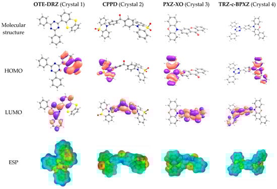
Figure 1.
Molecular structures, HOMO and LUMO patterns, and ESP distributions for the compounds studied.
3.2. Crystal Properties
Figure 2 shows the Hirshfeld surfaces mapped with curvedness for the crystals of studied compounds; the Hirshfeld surfaces mapped with ESP are shown in Figure S1 of the Supplementary Materials. We used the curvedness maps to analyze the crystal packing and identify the planar π-stacking arrangements via the relatively large green (i.e., flat) regions [42]. Two of the four studied compounds (oTE-DRZ and PXZ-CMO) crystallized in the triclinic system with the space group while the other two (CPPD and TRZ-c-BPXZ) crystallized in the monoclinic system with the space group; however, they did not demonstrate similar packing. The oTE-DRZ compound tended to form one-dimensional stacks (this can be clearly seen in the energy framework given in Figure S3a); the curvedness map in Figure 2a shows one extended green region per each side of the Hirshfeld surface, which indicated that it was a π-stack. It is important to mention that the π∙∙∙π contact area between the adjacent molecules extended to both the donor and acceptor moieties. The second compound (CPPD) also tended to form one-dimensional stacks (Figure S3b), but since the π∙∙∙π contact was centered around the twisted benzophenone acceptor part, it was very limited (small flat green region in the center of the molecule in Figure 2b). The relatively large green region on the donor part showed how the molecules from adjacent stacks formed a dimer with a π∙∙∙π contact. Figure 2c shows how the compound PXZ-XO formed dimers with π∙∙∙π contacts independently through the donor part and through the acceptor part: only one side of each Hirshfeld surface of the donor/acceptor moiety has a large green region in the figure. A similar dimerization with π∙∙∙π contacts was observed for the fourth compound (TRZ-BPXZ; Figure 2d): separately for the BPXZ part and for the TRZ part. Yet for both the PXZ-XO and TRZ-BPXZ compounds, some minor green regions were identified, which indicated modest π∙∙∙π contacts with other adjacent molecules. A full list of the intermolecular contacts is shown in Figure S2 of Supplementary Materials.
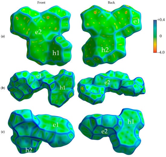
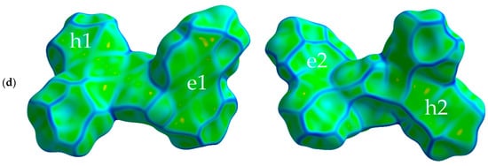
Figure 2.
Hirshfeld surfaces (front and back of the molecules) mapped with curvedness [28] for crystalline oTE-DRZ (a), CPPD (b), PXZ-XO (c), and TRZ-c-BPXZ (d). The blue color depicts edges (large curvature), the green color depicts relatively flat areas (curvature near unity), and the yellow and red colors depict super flat areas (curvature tended to zero). The labels depict the areas at the surface associated with important contacts for hole (“h”) and electron (“e”) transport.
3.3. Charge Transport
3.3.1. Transfer Integrals
oTE-DRZ (Crystal 1). The transfer integrals along various directions for all of the crystals studied are listed in Table 1. For oTE-DRZ, they are illustrated in Figure 3a,b. As mentioned above, this crystal differs from the others because it has a direction in which both donor and acceptor moieties form π-stacks. As follows from Figure 3a, large hole transfer integrals exceeding 80 meV were observed in this crystal; they formed a continuous charge transport path. Figure 3c illustrates that the abovementioned integrals corresponded to the π-stacking contacts of the molecules because the Hirshfeld surface for them is flat; these contacts also reveal themselves in Figure 2a (areas h1 and h2). The electron transfer integrals were much lower; the largest was 15 meV. As follows from Figure 3d, these integrals were observed for edge-to-edge molecular contacts (area e1 in Figure 2a). Surprisingly, the electron transfer integrals were negligible along the π-stack (i.e., for contacts associated with the green flat area (e2) in Figure 2a) despite the considerable overlap of the LUMO wavefunctions from the parallel and closely located triazine moieties (Figure S5b). This could be tentatively assigned to the phase mismatch between the two LUMOs in such π-stacking dimers (see Figure S6). Noteworthily, the LUMO+1 orbitals of the monomers showed JLUMO+1~110 meV for this dimer; the orbital of the dimer composed by the LUMO+1 orbitals of monomers (i.e., LUMO+2) was ~60 meV above its LUMO, and its population was just ~11 times lower than that of the latter. Thus, this orbital could participate in electron transport and increase the charge mobility by about two times.

Table 1.
Hole (Jh) and electron (Je) transfer integrals for the crystals studied.
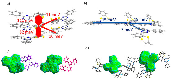
Figure 3.
Charge transfer integrals for hole (a) and electron (b) transport in oTE-DRZ crystal. (c,d) Intermolecular contacts that enable these transfer integrals; the left and right pictures correspond to the different sides of the central molecule. The Hirshfeld surface for the central molecule was mapped with curvedness. The coloring scale is depicted in Figure 2.
CPPD (Crystal 2). Transfer integrals for the CPPD crystal are shown in Figure 4a,b. Here, the donor moieties formed pairs with large hole transfer integrals (Jh ~ 150 meV), but these dimers were weakly electronically coupled to the donor moieties of the neighboring molecules (all other Jh < 5 meV) so that the continuous path of considerable Jh was not formed within the crystal. A large Jh was observed for the π-stacking contacts, which reveal themselves as flat green areas in Figure 4c (contact with the molecule colored in blue) and Figure 2b (area h1), in which the donor moieties lie one above another in an antiparallel manner with small lateral shifts. The acceptor moieties also formed tightly bound pairs with Je = 94 meV, and these dimers were coupled to the neighboring ones by a moderate Je = 26 meV, so a reasonable electron mobility could be expected for this crystal. Due to the twisted character of the BP acceptor moieties, their stacking was less pronounced (see areas e1 and e2 in Figure 2b and Figure 4d).
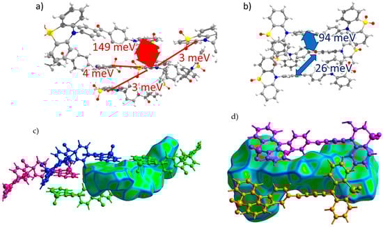
Figure 4.
Charge transfer integrals for hole (a) and electron (b) transport in CPPD crystal. (c,d) Intermolecular contacts that enable these transfer integrals. The Hirshfeld surface for the central molecule was mapped with curvedness. The coloring corresponds to Figure 2.
PXZ-XO (Crystal 3). Figure 5a,b show the transfer integrals for PXZ-XO. There were alternating transfer integrals of 47 and 23 meV for holes and 54 and 35 meV for electrons along the directions with the largest charge mobility. In both cases, a larger J corresponded to the face-to-face π-stacking contact with a smaller lateral shift (Figure 5c,d; areas h1 and e1 in Figure 2c). Noteworthily, the J value for the face-to-face dimer was in line with that calculated in Ref. [15] for a structurally close acridine–xanthone compound. A lower J corresponded to the face-to-face packing with a large lateral shift and hence a weaker orbital overlap; accordingly, the green flat areas at the Hirshfeld surface associated with these contacts as shown in Figure 2c and Figure 5c,d (areas h2 and e2) were smaller. The alternation in J was lesser than in Crystal 2, and the continuous paths of both the hole and electron transfer integrals enabled reasonable charge mobilities as shown below.
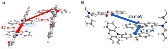
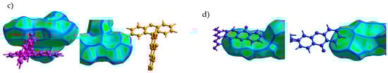
Figure 5.
Charge transfer integrals for hole (a) and electron (b) transport in PXZ-XO crystal. (c,d) Intermolecular contacts that enable these transfer integrals; the left picture corresponds to the contact that provided a larger J, while the right picture corresponds to the contact that provided a smaller J. The Hirshfeld surface for the central molecule was mapped with curvedness. The coloring corresponds to Figure 2.
TRZ-c-BPXZ (Crystal 4). The transfer integrals for TRZ-BPXZ are shown in Figure 6a,b. As shown in the figure, the hole transfer integrals were very small and did not exceed 10 meV. Curiously, they were small despite the face-to-face packing of the donor moieties (revealed by the large flat green areas in Figure 6c, left; and Figure 2d, area h2) with a large orbital overlap in one of the dimers; we attribute this to the phase mismatch of the overlapping HOMOs. As for the electrons, a considerable Je was observed for the two π-stacking contacts of the acceptor (TRZ) moieties (see areas e1 and e2 in Figure 2d and Figure 6d). There was a strong alternation in the Je along the stack of the TRZ moieties: one Je was extremely large and amounted to 172 meV, while the other was just 12 meV. This difference was associated with much smaller lateral shifts and hence a larger orbital overlap in the former case (the more extended contact in Figure 6d, left; and the larger flat area e1 in Figure 2d).
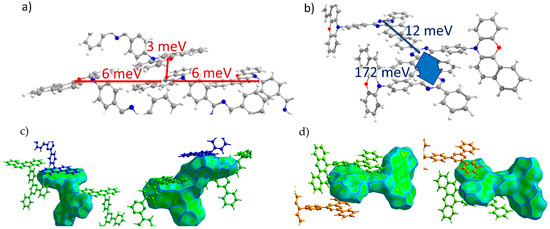
Figure 6.
Charge transfer integrals for hole (a) and electron (b) transport in TRZ-c-BPXZ crystal. (c,d) Intermolecular contacts that enable these transfer integrals; the left picture corresponds to the contact that provided a larger J, while the right picture corresponds to the contact that provided a smaller J. The Hirshfeld surface for the central molecule was mapped with curvedness. The coloring corresponds to Figure 2.
3.3.2. Reorganization Energies
The reorganization energies for the compounds studied are presented in Table 2. For oTE-DRZ, they amounted to 990 and 440 meV for the hole and electron transport, respectively. A huge reorganization energy for the hole transfer (cf. ~100 meV for high-mobility organic semiconductors such as pentacene and rubrene [43]) could be ascribed to the softness of a donor moiety that bears two sulfur atoms in the central six-member ring, which was in line with a large λ for TTF derivatives [44,45]. A smaller (but also large) electron reorganization energy could be explained by the higher rigidity and larger size (i.e., a better charge delocalization) of the acceptor moiety. For CPPD, the hole reorganization energy was much lower and amounted 220 meV, which could be ascribed to the relatively rigid annulated structure of its donor. In contrast, the electron reorganization energy was very large, presumably due to the small size and softness of the acceptor (BP) moiety. For PXZ-XO, both the hole and electron reorganization energies were moderate due to the annulated nature of the donor and acceptor and were comparable to anthracene (~250 meV), which has similar size. For TRZ-c-BPXZ, the hole reorganization energy was moderate, which could be also ascribed to the annulated structure of the BPXZ moiety. However, the electron reorganization energy was very large and was tentatively assigned to the considerable geometry changes at the bridge between the acceptor and donor moieties and the triazine ring.
Table 2.
Reorganization energies for hole and electron transfer in the crystals studied (in meV).
It is worth noting that the calculated values were upper-bound estimates for reorganization energies because they were obtained for isolated molecules; while in the crystal, neighboring molecules could restrict the geometric relaxation upon the charge transfer, especially the large-scale relative rotation of the donor and acceptor [14,44]. To show this, we calculated the reorganization energy for oTE-DRZ considering the impact of the crystal environment using the ONIOM approach [38]. Specifically, the molecule under investigation was surrounded by the neighboring molecules, and then the calculations necessary for λ estimation (see Section 2) were performed. DFT was applied for the central molecule, while its molecular shell was calculated using the composite HF-3C method. In this case, the reorganization energy decreased by about two times (see Table 2), which significantly increased the charge mobility (Table 3).
Table 3.
Charge carrier mobilities in the crystals studied.
3.3.3. Charge Mobilities
Table 3 shows the obtained charge carrier mobilities that were calculated using the J and λ values presented above. The calculated charge mobilities were much higher than those experimentally observed in many of the studies on pristine films of TADF luminophores (10−8–10−4 cm2/(V∙s) [14,15,16,17,46]) and comparable to those reported in a few other studies (~10−3–0.85 cm2/(V∙s) [22,23,46,47,48]). The discrepancy between the theoretical and most of the experimental charge mobilities could be easily explained by the presence of grain boundaries, defects, and contact issues that lowered the charge mobility in the experiment. As follows from Table 3, a relatively efficient ambipolar transport was predicted for PXZ-XO with µh = 0.39 cm2/(V∙s) and µe = 0.34 cm2/(V∙s). The considerable and comparable mobilities for the holes and electrons in this material could be ascribed to the comparable and relatively large (~1.5 kT; see Table 1) transfer integrals and moderate reorganization energies (less than 260 meV; see Table 2). The relatively large μh and μe for this compound were in line with the larger mobilities reported for some XO-based luminophores (μh,e ~10−2 cm2/(V∙s) in Ref. [48]) as compared to other TADF luminophores (μh,e ~10−4–10−8 cm2/(V∙s) in Refs. [16,17]). Moreover, for a compound that is structurally close to PXZ-XO, namely [3-(9,9-dimethylacridin-10(9H)-yl)-9H-xanthen-9-one], an electron mobility of 0.2 cm2/(V∙s), which was very close to our data (see Table 3), was obtained in field-effect transistors (although in a blend with an mCBP host that may play major role in charge transport) [22].
CPPD showed a considerable hole mobility that was mainly due to a small hole reorganization energy λh (220 meV; see Table 2), although the Jh showed a strong alternation along any direction. On the contrary, the electron mobility was an order lower than that of the hole due to the large electron reorganization energy λe (660 meV; see Table 2) despite the large Je. Note that kr and hence μ show an exponential dependence on λ, which follows from Equation (1); this explains the dominating impact of this parameter on charge mobility in the materials studied. The large difference between the μe and μh for CDDP was in line with Ref. [49], in which it was experimentally observed that the electron transport in a TADF luminophore film with BP as the acceptor unit was inferior to that of the hole. oTE-DRZ and TRZ-c-BPXZ showed low charge mobilities due to the absence of a continuous path of transfer integrals and/or a large reorganization energy. A larger electron mobility than that of the hole for the former compound stemmed from a lower electron reorganization energy as compared to that of the hole (see Table 2). Noteworthily, the abovementioned charge mobilities could be lower-bound estimates because they were obtained by using the reorganization energies that were calculated for single molecules without accounting for the restriction of the geometry relaxation by the environment. Indeed, considering the environment effect on λ using the ONIOM approach (see above) could result in a considerable increase in the charge mobility (as shown in Table 3) for oTE-DRZ: for holes, it increased by nearly two orders of magnitude and reached 0.08 cm2/(V∙s); while for electrons, it increased by about 20 times and reached 0.156 cm2/(V∙s). Moreover, for oTE-DRZ, the electron mobility would increase even more (by about two times) if the contribution of LUMO+1 was considered.
3.4. Outlook
Our analysis highlighted several structure-property relationships. First, both the donor and acceptor moieties of TADF luminophores should be rather rigid in order to have a small reorganization energy, which is very important for a high charge-carrier mobility. Second, as expected, if the donor (acceptor) moieties formed continuous π-stacks, a considerable hole (electron) mobility could be observed. Noteworthily, in oTE-DRZ, the donor and acceptor moieties form segregated stacks that are favorable for charge transport, probably due to the different shapes of the donor and acceptor (planar DRZ and kinked oTE, respectively). The tendency for face-to-face packing instead of herringbone packing could be ascribed to a non-uniform ESP (Figure 1) that introduced attractive electrostatic interactions between the parallel conjugated cores, which was in line with Refs. [50,51,52,53]. Third, in most of the crystals studied, the donor (acceptor) moieties tend to dimerize and form tightly bound pairs that weakly couple to each other. Accordingly, the transfer integrals are alternated along the charge transport path, thereby decreasing the mobility. This pairing could have stemmed from the asymmetrical ESP distribution at the donor (acceptor) moieties (see Figure 1), which implies a static dipole moment for them and facilitates their antiparallel packing. As a result, we hypothesized that for an efficient charge transport, TADF luminophores should have a planar annulated aromatic structure with an ESP distribution as symmetrical as possible.
It is worth noting that the reported charge mobilities above 10−3 cm2/(Vs) are low as compared to those for high-mobility organic semiconductors (for many of which the mobility exceeds 10 cm2/(V∙s) [43]) and amorphous silicon (μ~1 cm2/(V∙s))—the workhorses of state-of-the-art thin-film electronics. Nevertheless, the reported mobilities are appropriate for the operation of OLEDs, in which charges need to penetrate through a thin emission layer (several µm); this is corroborated by the reasonable performance of the devices reported in Refs. [6,7,8,9]. However, TADF luminophores are also promising for other types of light-emitting devices; e.g., OLETs [54]. In these devices, higher charge mobilities are required because the geometry of these devices differs significantly from OLEDs and requires the charge carriers to travel much longer distances prior to recombination. For instance, charge mobilities in the range 0.1–3 cm2/(V∙s) were reported for single crystals of organic semiconductors used in efficient OLETs [20]. Importantly, ambipolar charge transport is highly desirable for these devices because it enables efficient charge recombination inside the channel, and OLETs based on ambipolar organic semiconductors generally outperform those showing a single type of charge-carrier mobility. Thus, the relatively high and balanced electron and hole mobilities of ~0.3 cm2/(V∙s) predicted in this study for PXZ-XO highlight the feasibility of using non-doped films and single crystals of TADF luminophores as active layers in OLETs. Since this study addressed the charge transport in arbitrarily chosen crystals of TADF luminophores, we expect that an aimed search and a rational design will uncover such materials with higher charge mobilities.
4. Conclusions
We performed a comparative theoretical study of the molecular packing and charge transport in four crystals of TADF luminophores. We found that among the crystals studied, there was one with considerable mobilities of electrons and holes (~0.3 cm2/(V∙s)); in one crystal the hole mobility equaled ~0.03 cm2/(V∙s) and was much larger than that of the electrons, and in two crystals the hole and electron mobilities were comparable and low (less than 0.01 cm2/(V∙s)). Expectedly, the largest charge transfer integrals were observed for face-to-face molecular dimers with small lateral shifts; however, the bottleneck was the small transfer integral between pairs of these tightly interacting dimers in most of the crystals studied. The highest mobility was predicted for the compound in which the donor and acceptor were relatively small and annulated heteroaromatic moieties, which enabled a moderate reorganization energy and a moderate alternation in the transfer integrals in the highest-mobility direction. We anticipate that the results obtained will be useful for the design of non-doped OLEDs, OLETs, and other light-emitting devices.
Supplementary Materials
The following supporting information can be downloaded at: https://www.mdpi.com/article/10.3390/cryst13010055/s1, Figure S1: Hirshfeld surfaces (front and back of the molecules) mapped with electrostatic potential for crystals. Figure S2: Distribution of reciprocal intermolecular contacts for the crystals. Figure S3: Graphical representation of total sum of interactions in the crystals. Figure S4: Distribution of sum of interaction energies (absolute values) in crystals for 3.8Å cluster. Table S1: Different interaction energies of the molecular pairs for oTE-DRZ in kJ mol-1. Table S2: Different interaction energies of the molecular pairs for CPPD in kJ mol-1. Table S3: Different interaction energies of the molecular pairs for PXZ-XO in kJ mol-1. Table S4: Different interaction energies of the molecular pairs for TRZ-c-BPXZ in kJ mol-1. Figure S5: HOMO and LUMO of the oTE-DRZ π-stacking dimer. Figure S6. LUMO of the oTE-DRZ π-stack.
Author Contributions
Conceptualization, A.Y.S.; methodology, A.Y.S.; software, A.Y.S., D.I.D. and N.O.D.; validation, A.Y.S.; formal analysis, A.Y.S. and N.O.D.; investigation, A.Y.S., D.I.D. and N.O.D.; resources, A.Y.S.; data curation, A.Y.S.; writing—original draft preparation, A.Y.S. and D.I.D.; writing—review and editing, A.Y.S. and D.I.D.; visualization, A.Y.S. and D.I.D.; supervision, A.Y.S.; project administration, A.Y.S.; funding acquisition, A.Y.S. All authors have read and agreed to the published version of the manuscript.
Funding
The DFT calculations for single molecules, ONIOM calculations, crystal structure analysis and charge mobility calculations were financially supported by the Ministry of Science and Higher Education of the Russian Federation (project FFSM-2022-0004).
Data Availability Statement
Data available on request from the authors.
Conflicts of Interest
The authors declare no conflict of interest.
References
- Huang, Y.; Hsiang, E.-L.; Deng, M.-Y.; Wu, S.-T. Mini-LED, Micro-LED and OLED displays: Present status and future perspectives. Light Sci. Appl. 2020, 9, 105. [Google Scholar] [CrossRef] [PubMed]
- Salehi, A.; Fu, X.; Shin, D.-H.; So, F. Recent Advances in OLED Optical Design. Adv. Funct. Mater. 2019, 29, 1808803. [Google Scholar] [CrossRef]
- Lee, S.M.; Kwon, J.H.; Kwon, S.; Choi, K.C. A Review of Flexible OLEDs Toward Highly Durable Unusual Displays. IEEE Trans. Electron. Devices 2017, 64, 1922–1931. [Google Scholar] [CrossRef]
- Hsiang, E.-L.; Yang, Z.; Yang, Q.; Lan, Y.-F.; Wu, S.-T. Prospects and challenges of mini-LED, OLED, and micro-LED displays. J. Soc. Inf. Disp. 2021, 29, 446–465. [Google Scholar] [CrossRef]
- Cai, X.; Su, S.-J. Marching Toward Highly Efficient, Pure-Blue, and Stable Thermally Activated Delayed Fluorescent Organic Light-Emitting Diodes. Adv. Funct. Mater. 2018, 28, 1802558. [Google Scholar] [CrossRef]
- Cai, X.; Qiao, Z.; Li, M.; Wu, X.; He, Y.; Jiang, X.; Cao, Y.; Su, S.-J. Purely Organic Crystals Exhibit Bright Thermally Activated Delayed Fluorescence. Angew. Chem. Int. Ed. 2019, 58, 13522–13531. [Google Scholar] [CrossRef]
- Gužauskas, M.; Narbutaitis, E.; Volyniuk, D.; Baryshnikov, G.V.; Minaev, B.F.; Ågren, H.; Chao, Y.-C.; Chang, C.-C.; Rutkis, M.; Grazulevicius, J.V. Polymorph acceptor-based triads with photoinduced TADF for UV sensing. Chem. Eng. J. 2021, 425, 131549. [Google Scholar] [CrossRef]
- Zhang, Y.; Ma, H.; Wang, S.; Li, Z.; Ye, K.; Zhang, J.; Liu, Y.; Peng, Q.; Wang, Y. Supramolecular Structure-Dependent Thermally-Activated Delayed Fluorescence (TADF) Properties of Organic Polymorphs. J. Phys. Chem. C 2016, 120, 19759–19767. [Google Scholar] [CrossRef]
- Yang, W.; Yang, Y.; Cao, X.; Liu, Y.; Chen, Z.; Huang, Z.; Gong, S.; Yang, C. On-off switchable thermally activated delayed fluorescence controlled by multiple channels: Understanding the mechanism behind distinctive polymorph-dependent optical properties. Chem. Eng. J. 2021, 415, 128909. [Google Scholar] [CrossRef]
- Zhang, Y.; Li, Z.; Li, C.; Wang, Y. Suppressing Efficiency Roll-Off of TADF Based OLEDs by Constructing Emitting Layer with Dual Delayed Fluorescence. Front. Chem. 2019, 7, 302. [Google Scholar] [CrossRef]
- Han, J.; Huang, Z.; Miao, J.; Qiu, Y.; Xie, Z.; Yang, C. Narrowband blue emission with insensitivity to the doping concentration from an oxygen-bridged triarylboron-based TADF emitter: Nondoped OLEDs with a high external quantum efficiency up to 21.4%. Chem. Sci. 2022, 13, 3402–3408. [Google Scholar] [CrossRef]
- Zhao, G.; Liu, D.; Wang, P.; Huang, X.; Chen, H.; Zhang, Y.; Zhang, D.; Jiang, W.; Sun, Y.; Duan, L. Exceeding 30 % External Quantum Efficiency in Non-doped OLEDs Utilizing Solution Processable TADF Emitters with High Horizontal Dipole Orientation via Anchoring Strategy. Angew. Chem. Int. Ed. 2022, 61, e202212861. [Google Scholar] [CrossRef] [PubMed]
- Shi, Y.-Z.; Wu, H.; Wang, K.; Yu, J.; Ou, X.-M.; Zhang, X.-H. Recent progress in thermally activated delayed fluorescence emitters for nondoped organic light-emitting diodes. Chem. Sci. 2022, 13, 3625–3651. [Google Scholar] [CrossRef] [PubMed]
- Danyliv, Y.; Ivaniuk, K.; Danyliv, I.; Bezvikonnyi, O.; Volyniuk, D.; Galyna, S.; Lazauskas, A.; Skhirtladze, L.; Ågren, H.; Stakhira, P.; et al. Carbazole-σ-sulfobenzimide derivative exhibiting mechanochromic thermally activated delayed fluorescence as emitter for flexible OLEDs: Theoretical and experimental insights. Dyes Pigm. 2022, 208, 110841. [Google Scholar] [CrossRef]
- Ran, Y.; Yang, G.; Liu, Y.; Han, W.; Gao, G.; Su, R.; Bin, Z.; You, J. A methyl-shield strategy enables efficient blue thermally activated delayed fluorescence hosts for high-performance fluorescent OLEDs. Mater. Horiz. 2021, 8, 2025–2031. [Google Scholar] [CrossRef]
- Bucinskas, A.; Bezvikonnyi, O.; Gudeika, D.; Volyniuk, D.; Grazulevicius, J.V. Methoxycarbazolyl-disubstituted dibenzofuranes as holes- and electrons-transporting hosts for phosphorescent and TADF-based OLEDs. Dyes Pigm. 2020, 172, 107781. [Google Scholar] [CrossRef]
- Bezvikonnyi, O.; Gudeika, D.; Volyniuk, D.; Rutkis, M.; Grazulevicius, J.V. Diphenylsulfone-based hosts for electroluminescent devices: Effect of donor substituents. Dyes Pigm. 2020, 175, 108104. [Google Scholar] [CrossRef]
- Liu, C.; Huang, K.; Park, W.-T.; Li, M.; Yang, T.; Liu, X.; Liang, L.; Minari, T.; Noh, Y.-Y. A unified understanding of charge transport in organic semiconductors: The importance of attenuated delocalization for the carriers. Mater. Horiz. 2017, 4, 608–618. [Google Scholar] [CrossRef]
- Menard, E.; Podzorov, V.; Hur, S.-H.; Gaur, A.; Gershenson, M.E.; Rogers, J.A. High-Performance n- and p-Type Single-Crystal Organic Transistors with Free-Space Gate Dielectrics. Adv. Mater. 2004, 16, 2097–2101. [Google Scholar] [CrossRef]
- Qin, Z.; Gao, C.; Dong, H.; Hu, W. Organic Semiconductor Single-Crystal Light-Emitting Transistors. Adv. Opt. Mater. 2022, in press. [CrossRef]
- Fedorenko, R.S.; Kuevda, A.V.; Trukhanov, V.A.; Konstantinov, V.G.; Sosorev, A.Y.; Sonina, A.A.; Kazantsev, M.S.; Surin, N.M.; Grigorian, S.; Borshchev, O.V.; et al. Luminescent High-Mobility 2D Organic Semiconductor Single Crystals. Adv. Electron. Mater. 2022, 8, 2101281. [Google Scholar] [CrossRef]
- Ahmad, V.; Sobus, J.; Bencheikh, F.; Mamada, M.; Adachi, C.; Lo, S.-C.; Namdas, E.B. High EQE and High Brightness Solution-Processed TADF Light-Emitting Transistors and OLEDs. Adv. Opt. Mater. 2020, 8, 2000554. [Google Scholar] [CrossRef]
- Sobus, J.; Bencheikh, F.; Mamada, M.; Wawrzinek, R.; Ribierre, J.-C.; Adachi, C.; Lo, S.-C.; Namdas, E.B. High Performance p- and n-Type Light-Emitting Field-Effect Transistors Employing Thermally Activated Delayed Fluorescence. Adv. Funct. Mater. 2018, 28, 1800340. [Google Scholar] [CrossRef]
- Choi, H.H.; Cho, K.; Frisbie, C.D.; Sirringhaus, H.; Podzorov, V. Critical assessment of charge mobility extraction in FETs. Nat. Mater. 2018, 17, 2–7. [Google Scholar] [CrossRef]
- Yavuz, I.; Lopez, S.A.; Lin, J.B.; Houk, K.N. Quantitative prediction of morphology and electron transport in crystal and disordered organic semiconductors. J. Mater. Chem. C 2016, 4, 11238–11243. [Google Scholar] [CrossRef]
- Sokolov, A.N.; Atahan-Evrenk, S.; Mondal, R.; Akkerman, H.B.; Sánchez-Carrera, R.S.; Granados-Focil, S.; Schrier, J.; Mannsfeld, S.C.B.; Zoombelt, A.P.; Bao, Z.; et al. From computational discovery to experimental characterization of a high hole mobility organic crystal. Nat. Commun. 2011, 2, 437. [Google Scholar] [CrossRef]
- Schober, C.; Reuter, K.; Oberhofer, H. Virtual Screening for High Carrier Mobility in Organic Semiconductors. J. Phys. Chem. Lett. 2016, 7, 3973–3977. [Google Scholar] [CrossRef]
- Spackman, P.R.; Turner, M.J.; McKinnon, J.J.; Wolff, S.K.; Grimwood, D.J.; Jayatilaka, D.; Spackman, M.A. CrystalExplorer: A program for Hirshfeld surface analysis, visualization and quantitative analysis of molecular crystals. J. Appl. Crystallogr. 2021, 54, 1006–1011. [Google Scholar] [CrossRef]
- Turner, M.J.; Grabowsky, S.; Jayatilaka, D.; Spackman, M.A. Accurate and Efficient Model Energies for Exploring Intermolecular Interactions in Molecular Crystals. J. Phys. Chem. Lett. 2014, 5, 4249–4255. [Google Scholar] [CrossRef]
- Mackenzie, C.F.; Spackman, P.R.; Jayatilaka, D.; Spackman, M.A. CrystalExplorer model energies and energy frameworks: Extension to metal coordination compounds, organic salts, solvates and open-shell systems. IUCrJ 2017, 4, 575–587. [Google Scholar] [CrossRef]
- Marcus, R.A.; Sutin, N. Electron transfers in chemistry and biology. Biochim. Biophys. Acta—Bioenerg. 1985, 811, 265–322. [Google Scholar] [CrossRef]
- Baumeier, B.; Kirkpatrick, J.; Andrienko, D. Density-functional based determination of intermolecular charge transfer properties for large-scale morphologies. Phys. Chem. Chem. Phys. 2010, 12, 11103–11113. [Google Scholar] [CrossRef] [PubMed]
- Kirkpatrick, J. An approximate method for calculating transfer integrals based on the ZINDO Hamiltonian. Int. J. Quantum Chem. 2008, 108, 51–56. [Google Scholar] [CrossRef]
- Kobayashi, H.; Kobayashi, N.; Hosoi, S.; Koshitani, N.; Murakami, D.; Shirasawa, R.; Kudo, Y.; Hobara, D.; Tokita, Y.; Itabashi, M. Hopping and band mobilities of pentacene, rubrene, and 2,7-dioctyl[1]benzothieno[3,2-b][1]benzothiophene (C8-BTBT) from first principle calculations. J. Chem. Phys. 2013, 139, 014707. [Google Scholar] [CrossRef]
- Coropceanu, V.; Cornil, J.; da Silva Filho, D.A.; Olivier, Y.; Silbey, R.; Brédas, J.-L. Charge Transport in Organic Semiconductors. Chem. Rev. 2007, 107, 926–952. [Google Scholar] [CrossRef]
- Schmidt, M.W.; Baldridge, K.K.; Boatz, J.A.; Elbert, S.T.; Gordon, M.S.; Jensen, J.H.; Koseki, S.; Matsunaga, N.; Nguyen, K.A.; Su, S.; et al. General atomic and molecular electronic structure system. J. Comput. Chem. 1993, 14, 1347–1363. [Google Scholar] [CrossRef]
- Gordon, M.S.; Schmidt, M.W. Chapter 41—Advances in electronic structure theory: GAMESS a decade later. In Theory and Applications of Computational Chemistry; Dykstra, C.E., Frenking, G., Kim, K.S., Scuseria, G.E., Eds.; Elsevier: Amsterdam, The Netherlands, 2005; pp. 1167–1189. [Google Scholar]
- Chung, L.W.; Sameera, W.M.C.; Ramozzi, R.; Page, A.J.; Hatanaka, M.; Petrova, G.P.; Harris, T.V.; Li, X.; Ke, Z.; Liu, F.; et al. The ONIOM Method and Its Applications. Chem. Rev. 2015, 115, 5678–5796. [Google Scholar] [CrossRef]
- Sure, R.; Grimme, S. Corrected small basis set Hartree-Fock method for large systems. J. Comput. Chem. 2013, 34, 1672–1685. [Google Scholar] [CrossRef]
- Chemcraft. Graphical Software for Quantum Chemical Computations. Available online: https://www.chemcraftprog.com/ (accessed on 15 November 2022).
- Jmol: An Open-Source Java Viewer for Chemical Structures in 3D. Available online: http://www.jmol.org/ (accessed on 15 November 2022).
- McKinnon, J.J.; Spackman, M.A.; Mitchell, A.S. Novel tools for visualizing and exploring intermolecular interactions in molecular crystals. Acta Crystallogr. B 2004, 60, 627–668. [Google Scholar] [CrossRef]
- Ostroverkhova, O. Organic Optoelectronic Materials: Mechanisms and Applications. Chem. Rev. 2016, 116, 13279–13412. [Google Scholar] [CrossRef]
- Mas-Torrent, M.; Hadley, P.; Bromley, S.T.; Ribas, X.; Tarrés, J.; Mas, M.; Molins, E.; Veciana, J.; Rovira, C. Correlation between Crystal Structure and Mobility in Organic Field-Effect Transistors Based on Single Crystals of Tetrathiafulvalene Derivatives. J. Am. Chem. Soc. 2004, 126, 8546–8553. [Google Scholar] [CrossRef] [PubMed]
- Sosorev, A.Y. Simple charge transport model for efficient search of high-mobility organic semiconductor crystals. Mater. Des. 2020, 192, 108730. [Google Scholar] [CrossRef]
- Andruleviciene, V.; Leitonas, K.; Volyniuk, D.; Sini, G.; Grazulevicius, J.V.; Getautis, V. TADF versus TTA emission mechanisms in acridan and carbazole-substituted dibenzo[a,c]phenazines: Towards triplet harvesting emitters and hosts. Chem. Eng. J. 2021, 417, 127902. [Google Scholar] [CrossRef]
- Masimukku, N.; Gudeika, D.; Volyniuk, D.; Bezvikonnyi, O.; Simokaitiene, J.; Matulis, V.; Lyakhov, D.; Azovskyi, V.; Gražulevičius, J.V. Bipolar 1,8-naphthalimides showing high electron mobility and red AIE-active TADF for OLED applications. Phys. Chem. Chem. Phys. 2022, 24, 5070–5082. [Google Scholar] [CrossRef] [PubMed]
- Chen, J.; Zeng, J.; Zhu, X.; Guo, J.; Zhao, Z.; Tang, B.Z. Versatile Aggregation-Enhanced Delayed Fluorescence Luminogens Functioning as Emitters and Hosts for High-Performance Organic Light-Emitting Diodes. CCS Chem. 2021, 3, 230–240. [Google Scholar] [CrossRef]
- Liu, H.; Liu, H.; Fan, J.; Guo, J.; Zeng, J.; Qiu, F.; Zhao, Z.; Tang, B.Z. An Effective Design Strategy for Robust Aggregation-Induced Delayed Fluorescence Luminogens to Improve Efficiency Stability of Nondoped and Doped OLEDs. Adv. Opt. Mater. 2020, 8, 2001027. [Google Scholar] [CrossRef]
- Watt, M.; Hardebeck, L.K.E.; Kirkpatrick, C.C.; Lewis, M. Face-to-Face Arene−Arene Binding Energies: Dominated by Dispersion but Predicted by Electrostatic and Dispersion/Polarizability Substituent Constants. J. Am. Chem. Soc. 2011, 133, 3854–3862. [Google Scholar] [CrossRef]
- Trukhanov, V.A.; Dominskiy, D.I.; Parashchuk, O.D.; Feldman, E.V.; Surin, N.M.; Svidchenko, E.A.; Skorotetcky, M.S.; Borshchev, O.V.; Paraschuk, D.Y.; Sosorev, A.Y. Impact of N-substitution on structural, electronic, optical, and vibrational properties of a thiophene–phenylene co-oligomer. RSC Adv. 2020, 10, 28128–28138. [Google Scholar] [CrossRef]
- Sosorev, A.; Dominskiy, D.; Chernyshov, I.; Efremov, R. Tuning of Molecular Electrostatic Potential Enables Efficient Charge Transport in Crystalline Azaacenes: A Computational Study. Int. J. Mol. Sci. 2020, 21, 5654. [Google Scholar] [CrossRef]
- Sosorev, A.Y.; Trukhanov, V.A.; Maslennikov, D.R.; Borshchev, O.V.; Polyakov, R.A.; Skorotetcky, M.S.; Surin, N.M.; Kazantsev, M.S.; Dominskiy, D.I.; Tafeenko, V.A.; et al. Fluorinated Thiophene-Phenylene Co-Oligomers for Optoelectronic Devices. ACS Appl. Mater. Interfaces 2020, 12, 9507–9519. [Google Scholar] [CrossRef]
- Qin, Z.; Gao, H.; Dong, H.; Hu, W. Organic Light-Emitting Transistors Entering a New Development Stage. Adv. Mater. 2021, 33, 2007149. [Google Scholar] [CrossRef] [PubMed]


Disclaimer/Publisher’s Note: The statements, opinions and data contained in all publications are solely those of the individual author(s) and contributor(s) and not of MDPI and/or the editor(s). MDPI and/or the editor(s) disclaim responsibility for any injury to people or property resulting from any ideas, methods, instructions or products referred to in the content. |
© 2022 by the authors. Licensee MDPI, Basel, Switzerland. This article is an open access article distributed under the terms and conditions of the Creative Commons Attribution (CC BY) license (https://creativecommons.org/licenses/by/4.0/).