1. Introduction
Transparent conductive oxides (TCO) are actively being adopted as the conductive films in modern optoelectronic devices, such as panels, solar cell, organic light emitting diodes, and gas sensors. Indium tin oxide (ITO) is an auspicious TCO material with high transparency and low resistivity, which is widely adopted in optoelectronic applications [
1,
2]. Parallelly, pure and impurity-doped zinc oxide (ZnO) materials are considered as advantageous alternatives for replacing ITO. ZnO is a compound metal-oxide semiconductor with a wurtzite hexagonal structure, which has high thermal conductivity, good electrical features, high transparency, large exciton binding energy (E = 60 meV), and a high bandgap (
Eg = 3.37 eV). These characteristics render ZnO a promising substitution material for ITO [
3,
4,
5,
6].
Due to its high adsorption of atmospheric oxygen, the resistivity of pure ZnO cannot be decreased easily. The addition of impurity elements to ZnO can effectively stabilise its interstitial zinc and oxygen vacancies and reduce its resistivity, thereby enhancing its electrical properties [
7]. Different dopants have been investigated, such as boron [
8,
9], aluminium [
10,
11], indium [
12], gallium [
13,
14], and fluorine [
15,
16]. Despite the above, the studies on doping other metal elements on ZnO films remain limited. Firooz et al. employed multiple dopant elements, e.g., Cr, Mn, Fe, Co, Cu, and Ni, to synthesise doped ZnO films using a hydrothermal method [
17]. Ngom et al. utilised pulse laser deposition (PLD) to fabricate 1.0 wt.% tungsten-doped ZnO (WZO) films with transparencies exceeding 80%, while their bandgaps were kept between 3.31 and 3.36 eV [
18]. Zhang et al. utilised a sputtering technique to fabricate 7.0 wt.% WZO films with a resistivity of 10
−4 Ω-cm [
19]. Accordingly, Chen et al. manufactured 1.5 wt.% WZO films with enhanced carrier mobility by using a 2-stage sputtering process with 2 sputtering powers [
20].
In this study, 1.0 wt.% WZO films were fabricated under various growth temperatures (200–400 °C) by utilising a pulse laser deposition technique. The optical, electrical, morphological, and structural properties of the WZO films were studied and discussed. Further, to elucidate the variation trend between the W-doping percentage and the carrier mobility of the films, their electrical properties were investigated under different W-doping percentages (0–9.0 wt.%) and a constant growth temperature (300 °C). Finally, pristine ZnO and WZO films were comparatively examined by X-ray photoelectron spectroscopy (XPS) analysis to determine the compositional distribution of Zn, O, and W elements; also, the results highlighted the film’s properties both before and after W-doping under different growth temperatures (250–350 °C).
2. Materials and Methods
In this work, a PLD technique was employed to fabricate a pristine ZnO film under a fixed growth temperature (300 °C), as well as WZO films with various W-doping percentages (1.0–9.0 wt.%) and under different growth temperatures. PLD is a promising technology that offers several advantages, such as good crystallisation efficiency, precise thickness control, high molecular energy, and ensures relatively identical doping percentages on both the target and film [
21]. Here, we employed a high-frequency KrF excimer laser with a 248 nm wavelength. The pulse energy and pulse frequency were set at 1.5 Jcm
−2 and 2 Hz, respectively. The distance between the target and the glass substrate was adjusted at 50 mm. The working chamber pressure was set above 10
−5 Pa, and the growth temperatures varied between 200 and 400 °C. The deposition time was 30 min to ensure that the thicknesses of the ZnO and WZO films were controlled at approximately 75–90 nm.
The ZnO and WZO targets (with different W-doping percentages) were fabricated using a solid-state sintering process. For example, to prepare the 1.0 wt.% WZO target, ZnO powder (99.0 wt.% ratio, 99.99% purity) and tungsten power (1.0 wt.% ratio, 99.99% WO3 purity) were put into a clean bottle and well-mixed by utilising a rolling machine for a period. After the powders were mixed, they were put into a cylinder mould (6 mm thickness, 22 mm diameter) and pressed at 5 tons for 15 min. The sintering of the WZO target was performed in two stages: first, the targets were heated from room temperature to 800 °C in a furnace tube, with a heating rate of 180 °C/h. Then, the temperature was kept at 800 °C for 6 h, and then gradually decreased to room temperature with a cooling rate of 3–5 °C/min. After the first stage was completed, the targets were pulverised, and the sintering process was performed once again. In the second stage, the same process was repeated, except that highest sintering temperature was raised to 1000 °C.
Glass substrates with dimensions of 1.5 × 0.5 cm, provided from Coning Eagle 2000, were used to deposit the thin films. Before starting the deposition process, the glass substrates were cleaned in 3 steps: first, the substrates were put into acetone and clean by using ultrasonic cleaner for ~10 min. Second, the glass substrates were put into de-ionised water and clean by using ultrasonic cleaner again for 10 min. The third step was to put the glass substrates into methanol and clean by using ultrasonic cleaner for 10 min. After all steps were completed, the glass substrates were dried using nitrogen gas.
Before deposition, the crystalline features of the pure ZnO and 1.0 wt.% WZO targets were examined by X-ray diffraction (XRD, Empyrean, Panalytical, Malvern, UK) analysis. Various analyses were used to study the ZnO film (growth temperature = 300 °C) and 1.0 wt.% WZO films (growth temperatures = 200–400 °C): their electrical characteristics were examined using the Hall Effect, and their surface morphologies were analysed using scanning electron microscopy (SEM). Their optical properties were determined by studying their transparencies (Jasco V550) and photoluminescence spectra (PL), and their structural properties were confirmed by XRD analysis. The elemental compositions and chemical states of the films’ surfaces were investigated by X-ray photoelectron spectroscopy (XPS, JPS-9030, JEOL), with an Mg anode as an X-ray source. The working pressure was 7 × 10⁻⁸ Pa, and Zn, O, and W elements were scanned and analysed. More importantly, the XPS results of the pure ZnO film (growth temperature = 300 °C) and WZO films were comparatively reviewed in terms of Zn and O contents, to determine the influence of these elements on the corresponding films’ properties.
3. Results and Discussion
3.1. Structural Properties
The structural properties of the ZnO and 1.0 wt.% WZO targets were examined by XRD analysis.
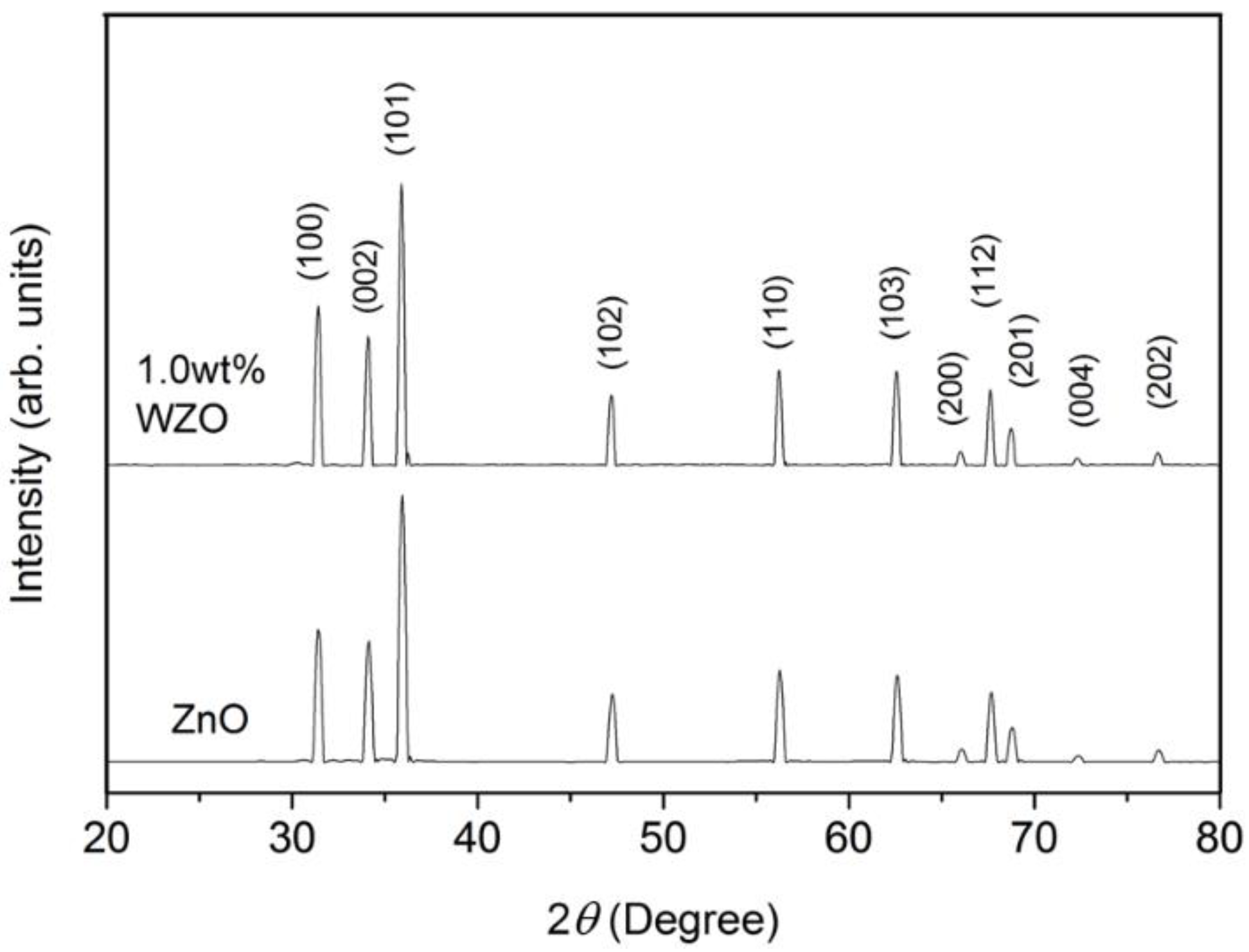
Figure 1 illustrates the correspondence between the diffraction peaks and the diffraction 2
θ angles. The peaks were located at 31.38°, 34.14°, 35.95°, 47.22°, 56.28°, 62.58°, 66.13°, 67.7°, 68.81°, 72.35°, and 76.68°, which were, respectively, ascribed to the (100), (002), (101), (102), (110), (013), (200), (112), (201), (004), and (202) crystalline planes. These planes correspond to the JCPDS Card 361451.
Figure 2 shows the XRD patterns of the 1.0 wt.% WZO thin films deposited at different growth temperatures (200–400 °C). The results indicated that the (002) diffraction peak appeared in all films approximately at 33.6°–34.2°. Furthermore, the (004) diffraction peak was obviously observed at ~72°–73° when the growth temperature varied between 350 and 400 °C. These results verified that all WZO thin films preserved the hexagonal wurtzite structure of ZnO. No other diffraction peaks appeared in the XRD patterns, suggesting that W atoms had been successfully incorporated into the films’ structure and acted as substitutional sites to ZnO [
22,
23,
24].
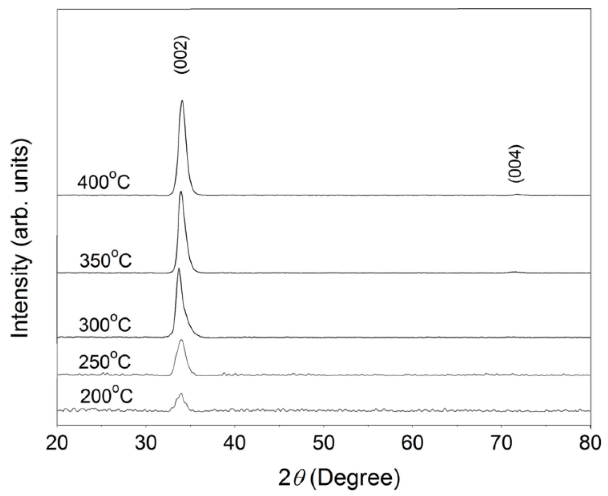
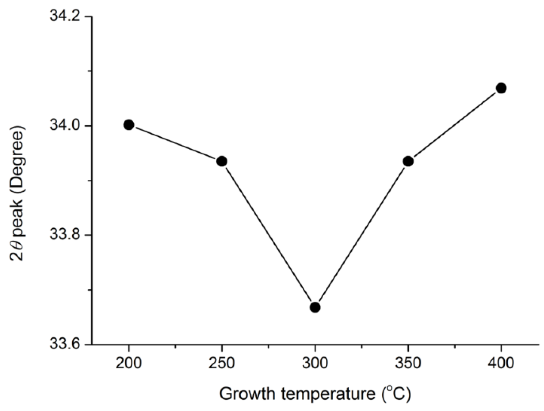
Figure 3 illustrates the (002) diffraction peak profile of the 1.0 wt.% WZO films grown under 200–400 °C. Notably, both the degree and intensity of the (002) diffraction peak shifted towards higher values as the growth temperatures rose from 300 to 400 °C. The ionic radius of W
6+ was approximately 64 pm, which was smaller than that of Zn
2+ (74 pm); this allowed the W
6+ atoms to effectively penetrate the ZnO crystalline lattice, and substitute the Zn
2+ atoms [
18,
22,
24].
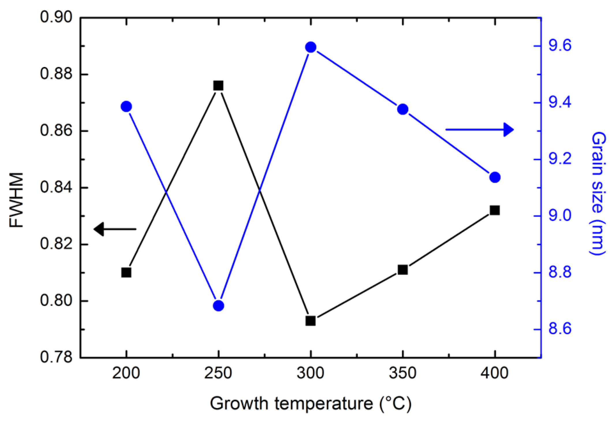
Figure 4 shows the grain size distribution of the 1.0 wt.% WZO films grown between 200 and 400 °C. The grain size was calculated by the full width at half maximum (FWHM) of the (002) diffraction peak according to the Debye-Scherrer formula [
25]. The grain sizes ranged between 8.6 and 9.6 nm, and became bigger when the growth temperature was 300 °C. However, the trend of the FWHM was opposite to that of the grain sizes ranging between 0.79 and 0.89. Particularly, the smallest FWHM value was calculated when the growth temperature was 300 °C.
3.2. Surface Morphology
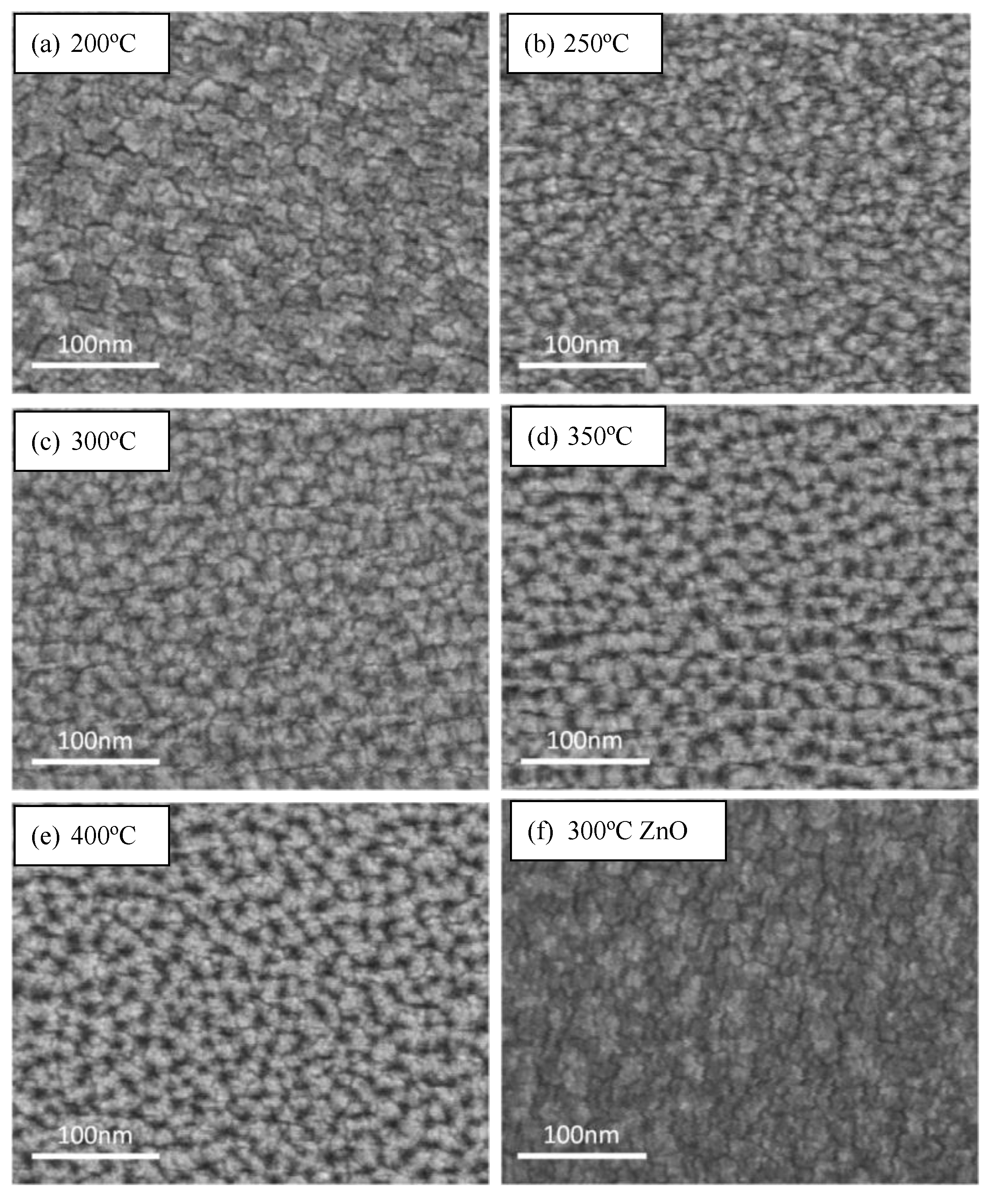
The SEM images of the 1.0 wt.% WZO films deposited at 200–400 °C are displayed in
Figure 5a–e. According to the images, all these films exhibited smooth surfaces. In addition,
Figure 5f shows the SEM image of the undoped ZnO film deposited at 300 °C, which demonstrated a similar surface morphology to that of the WZO film deposited at 200 °C.
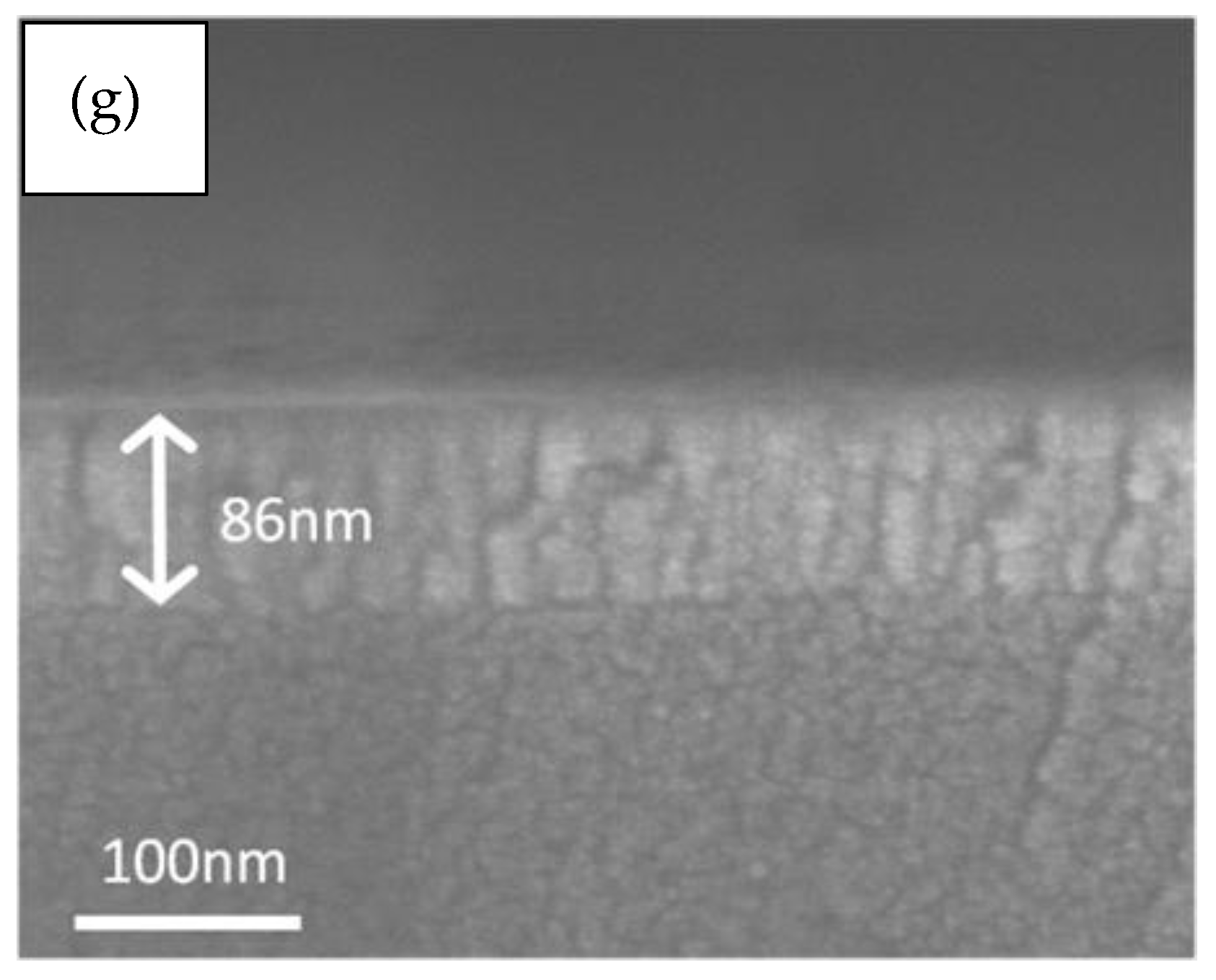
Figure 5g presents the cross-sectional view of the 1.0 wt.% WZO film deposited at 300 °C, whose thickness was measured at approximately 86 nm.
3.3. Electrical Properties
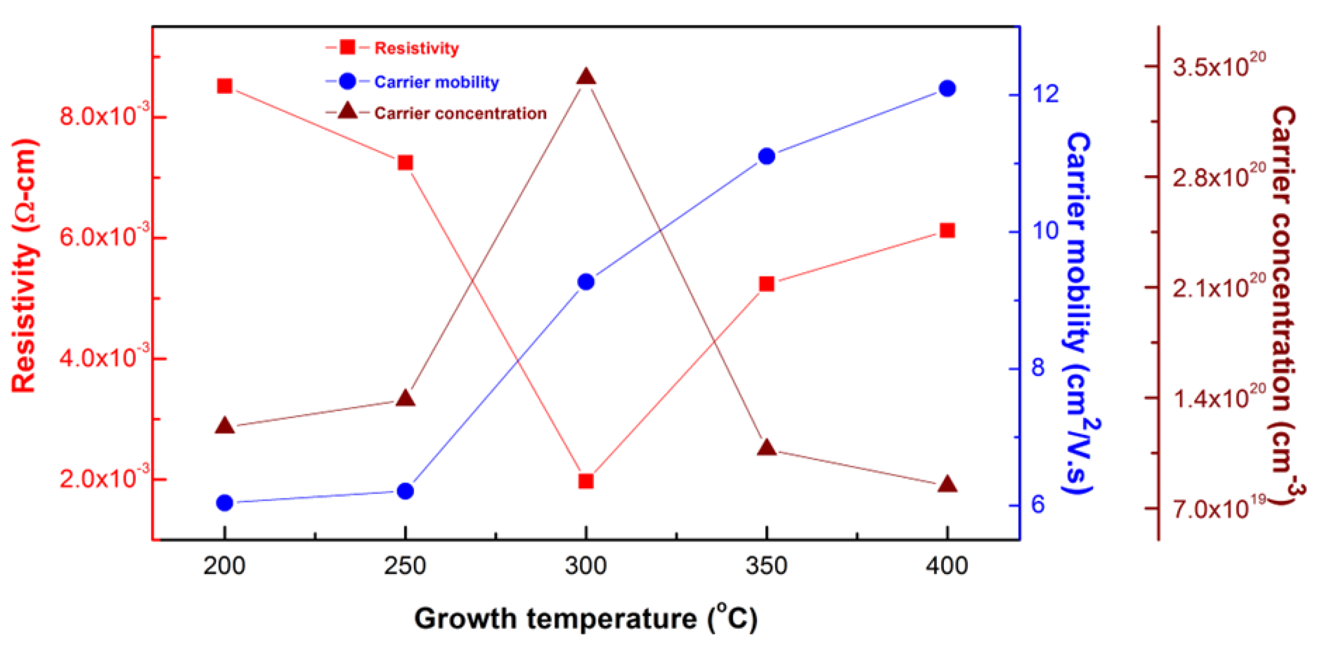
The electrical characteristics, namely carrier mobility, carrier concentration, and resistivity of the 1.0 wt.% WZO films deposited at 200–400 °C are illustrated in
Figure 6. At a growth temperature of 300 °C, the resistivity reached its lowest value (1.97 × 10
−3 Ω-cm), while the carrier mobility and carrier concentration were 9.27 cm
2/V·s and 3.42 × 10
20 cm
−3, respectively. Evidently, the carrier mobility increased along with the growth temperature. This shifting trend was theoretically attributed to the occurrence of scattering (stemming from the intra-grain clusters), combined with the presence of ionised impurity elements, and other factors. The carrier concentration showed an upward shifting trend as the growth temperature increased from 200 to 300 °C, where it reached its highest value. This behaviour was ascribed to the substitution of Zn with W atoms as follows: owing to their similar ionic radii, the W
6+ ions infiltrated the Zn
2+ sites and donated free carriers to the ZnO lattice, thus realising a conduction mechanism. Other factors, such as impurity scattering and crystalline defects, were also believed to have contributed to this trend [
25].
Table 1 comparatively summarises the electrical characteristics of the pure ZnO and 1.0 wt.% WZO films fabricated at 300 °C. As can be seen, the resistivity of the 1.0 wt.% WZO film was almost 2 times lower than that of the pure ZnO film. Parallelly, the carrier mobility and concentration of the former surpassed those of the latter. In view of the above, it was theorised that the electrical properties of the WZO film during fabrication were dominated by its oxygen vacancies and interstitial atoms, with the W atoms acting as donors to substitute the oxygen vacancies and zinc atoms [
26].
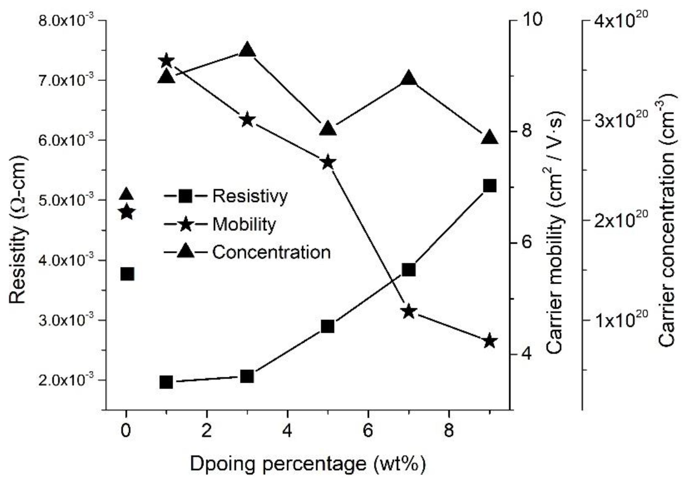
WZO films with different W-doping percentages, ranging from 3.0 to 9.0 wt.%, were fabricated under a growth temperature of 300 °C, and their electrical properties were compared with those of the 1.0 wt.% WZO film (
Figure 7). The results indicated that the carrier concentration remained stably between 2.81 and 3.68 × 10
20 cm
−3. This was theoretically ascribed to the stable growth temperature that constantly provided energy for the incorporation of W
6+ ions by substituting Zn
2+ ions. The carrier mobility showed a downward trend as the W-doping percentage increased, which was ascribed to the scattering mechanism comprising neutral impurity scattering, intragrain cluster scattering, ionised impurity scattering, grain-boundary scattering, lattice vibration scattering, etc. The ionised impurity scattering mobility was inversely proportional to the carrier concentration. When the carrier concentration was close to or above 1 × 10
20 cm
−3, the scattering mechanism was dominated by ionised impurity scattering. Accordingly, intragrain cluster scattering also greatly contributed to the decrease of the carrier mobility. A heavy W-doping percentage can enhance W-ion incorporation and facilitate the formation of intragrain clusters, such as W-O and W-W. These intragrain clusters were suspected to affect both the inclusion of active dopants and the carrier mobility, thus contributing to the increase of the scattering centre. This behaviour, that resulted in the decrease of the carrier mobility, was suspected to stem from the higher incorporation of ZnO and W species [
25,
27].
3.4. Optical Properties
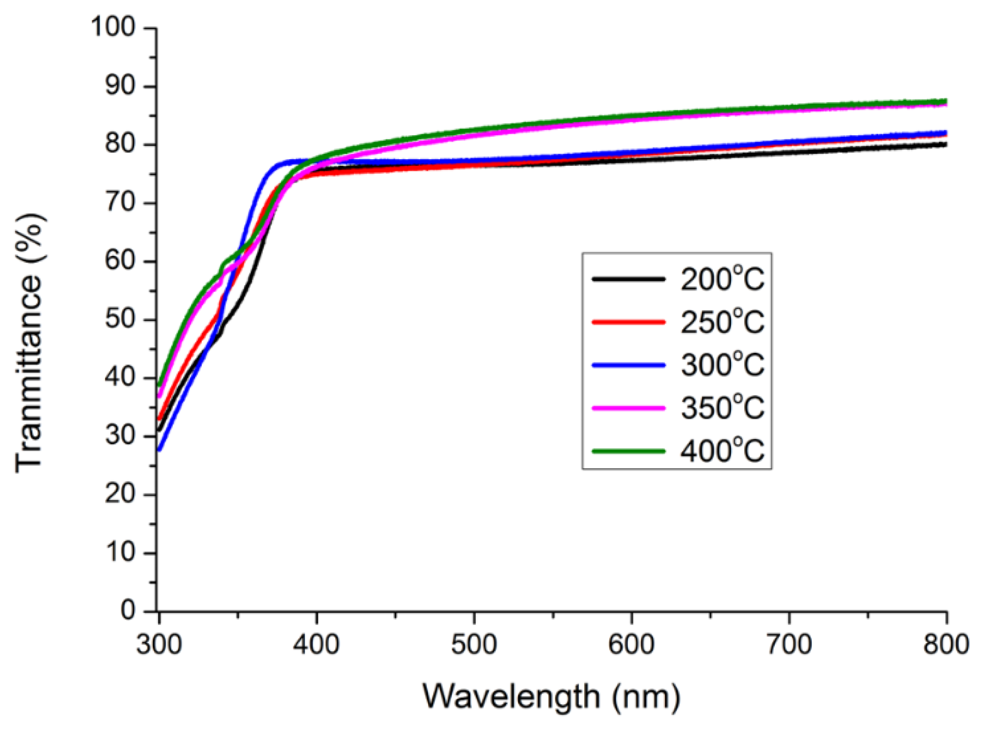
The transmittance results in the 300–800 nm wavelength range of the 1.0 wt.% WZO films deposited at 200–400 °C (
Figure 8) indicated that the transparencies of all films exceeded 75%. Their transparencies at the specific wavelengths of blue (460 nm), green (550 nm), and red (700 nm) are summarised in
Table 2. When the growth temperature varied between 200 and 300 °C, the differences in terms of transmittance between blue and red light were approximately 2.2–3.4%. These stable transmittance rates facilitate the stabilisation of incident light penetrating the WZO films. In addition, all WZO films exhibited a transmittance rate above 70% in the 375–400 nm range, that belongs to the ultraviolet (UV) region. Specifically, the transmittance of the 1.0 wt.% WZO film deposited at 300 °C remained above 70% when the incident wavelength was 360 nm.
ZnO is a material with semiconductor characteristics and a direct bandgap.
Figure 9a illustrates the bandgaps of the 1.0 wt.% WZO films (grown at 200–400 °C), with a dependence of (
αhν)
2, versus the photo energy (
Eg =
hν);
h is the Planck constant,
α is the absorption coefficient, and
v is the incident light frequency. The absorption coefficient
α can be calculated by the following equation:
where
R is the reflectance,
T is the transmittance,
λ is the wavelength,
t is the film thickness, and
α(
λ) is the absorption coefficient of different
λ. Here, the thicknesses of the 1.0 wt.% WZO films varied between 70 and 90 nm. The absorption coefficient
α and photo energy
Eg can be derived from the Tauc relation:
where
A is constant and
Eg is the bandgap energy [
2,
6]. The energy bandgaps of the 1.0 wt.% WZO films deposited at 200–400 °C were estimated by extrapolating the linear region of the graph to the photon energy axis; in this manner, the bandgap results ranged between 3.21 and 3.35 eV. This bandgap energy variation was theoretically attributed to the Burstein-Moss (BM) effect. The BM effect occurs when the carrier concentration surpasses the bottom density of the conduction band. This bandgap-shifting behaviour, that comprising a broadening and narrowing effect and typically manifests under a high-concentration doping state, is theorised to be caused by carrier-impurities and carrier-carrier scattering [
25]. As a result, the highest carrier concentration was achieved for the 1.0 wt.% WZO film deposited at 300 °C, which had the lowest resistivity among all WZO films. Furthermore, the bandgaps and transparencies of the films increased in the 351–396 nm wavelength range.
Figure 9b compares the bandgaps of the ZnO and 0.1 wt.% WZO films grown at 300 °C. As can be seen, the bandgap 1.0 wt.% WZO films surpassed that of the pristine ZnO film. The 1.0 wt.% WZO film grown at 300 °C possessed a very high bandgap energy and the lowest resistivity, that conjointly stemmed from its high carrier concentration; in turn, the high carrier concentration was associated with certain interference factors, such as the presence of excess metal ions and oxygen vacancies [
28].
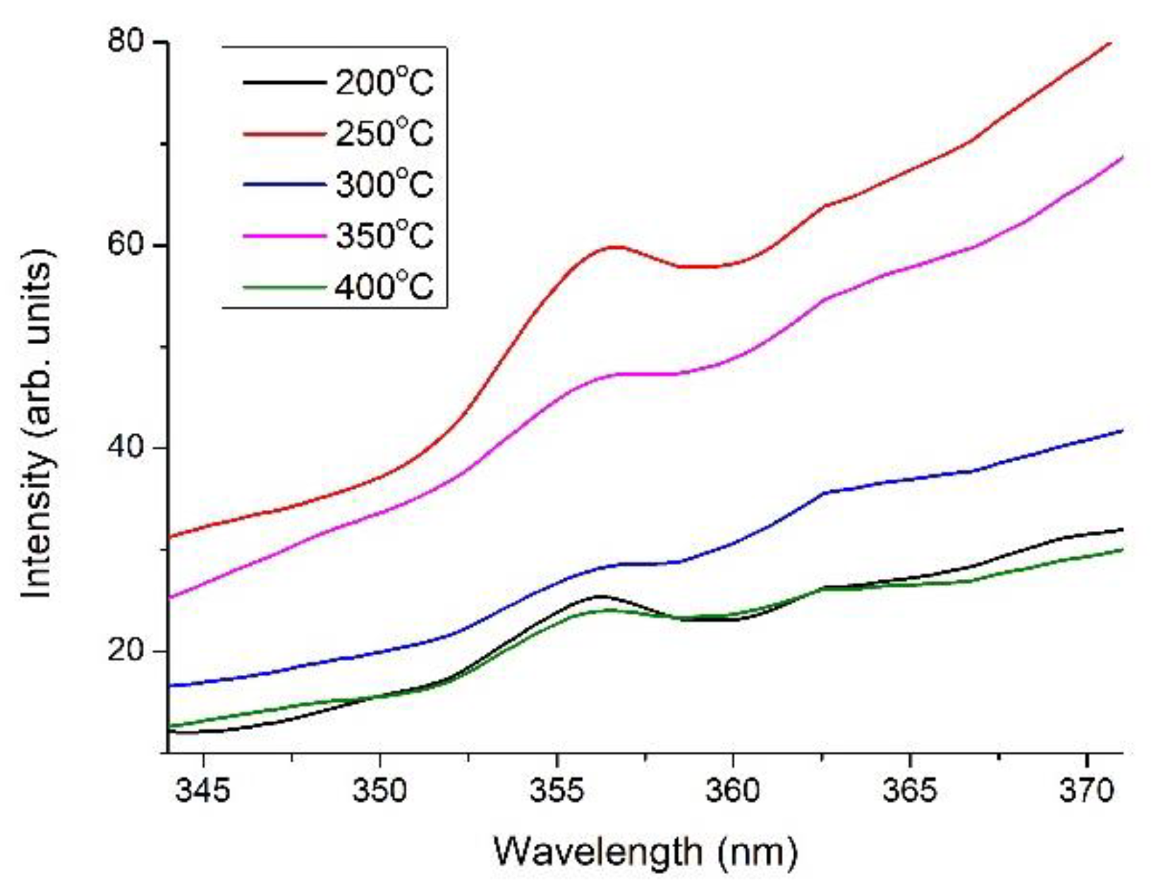
The PL spectra in the 343–371 nm wavelength range of the pure-glass substrates and 1.0 wt.% WZO films grown at 200–400 °C are illustrated in
Figure 10. The PL spectra were obtained using an excitation source of 266 nm with a resolution of 0.025 nm. All PL peaks appeared between 356.1 and 356.9 nm, a phenomenon that was ascribed to the UV near-band-edge transition of the WZO films; this was also reflected in the quality of the WZO films’ crystallinity. We hypothesised that the UV near-band-edge emission hindered the recombination of free excitons, resulting in several intrinsic defects in the potential well, such as interstitial sites, free holes, and oxygen vacancies [
29]. Further, the peak intensities became stronger as the growth temperature rose from 200 to 300 °C, stemming from the higher substrate temperatures that provided additional energy for free exciton recombination [
30].
3.5. XPS Analysis
The binding energy values were corrected by charging effects and are utilised by adventitious carbon value of C 1s result as reference, which is 284.8 eV [
31]. The XPS spectra of the O, Zn, and W elements were determined using Gaussian fitting, to identify the centred peaks.
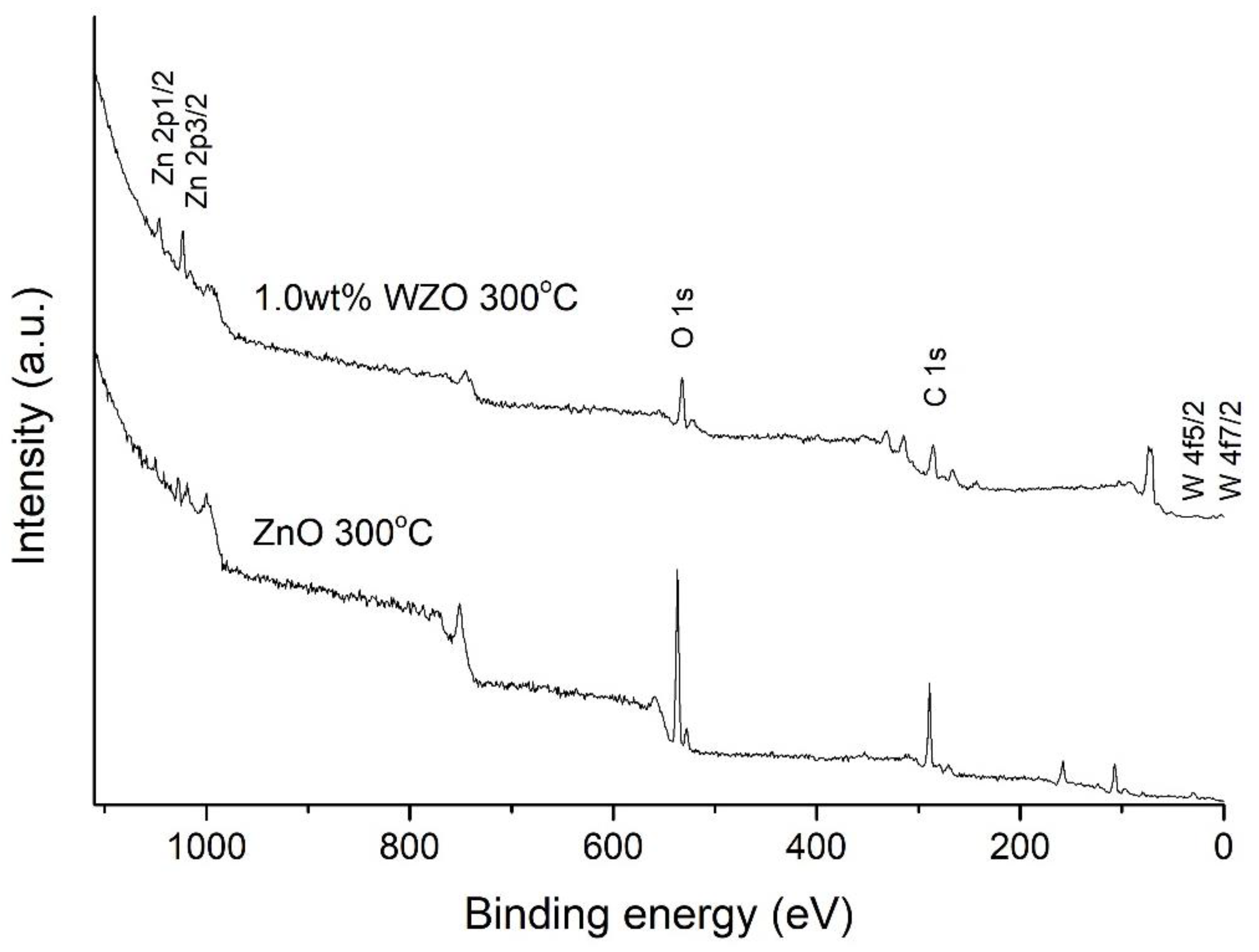
Figure 11 shows the XPS spectra of the ZnO and 1.0 wt.% WZO films grown at 300 °C, with full-length-scanning from 0 to 1100 eV. The results indicated that the intensities of the O 1s, C 1s, Zn 2p1/2, and Zn 2p3/2 peaks were strong, whereas the intensities of the W 4f5/2 and 7/2 peaks were weak; as such, the latter were difficult to identify from the full-scan spectra.
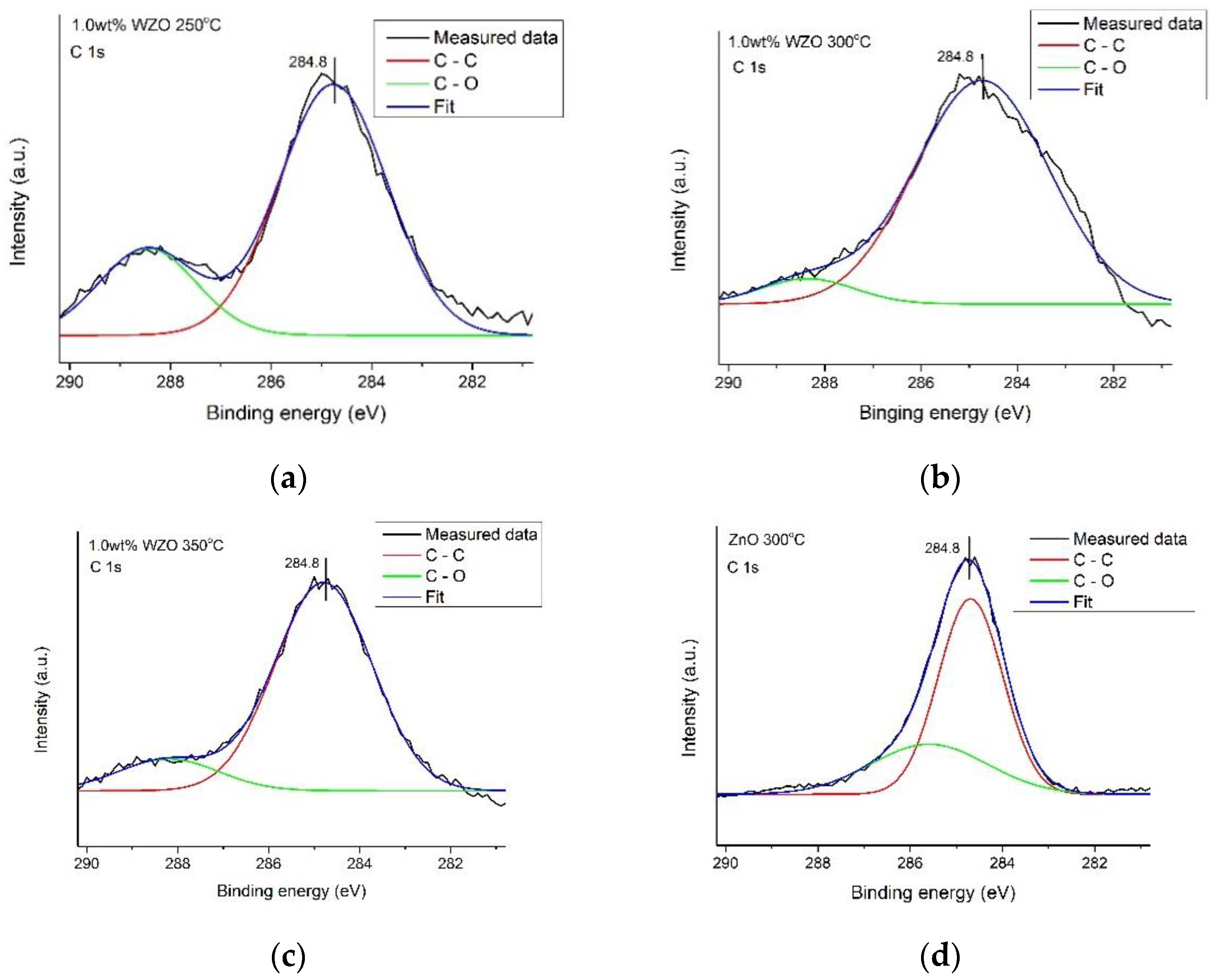
The C 1s XPS peaks of the 1.0 wt.% WZO films grown at 250 °C, 300 °C, and 350 °C, and ZnO film grown at 300 °C, are illustrated in
Figure 12. The peaks corresponding to the C-C and C-O bonds can also be identified [
32].
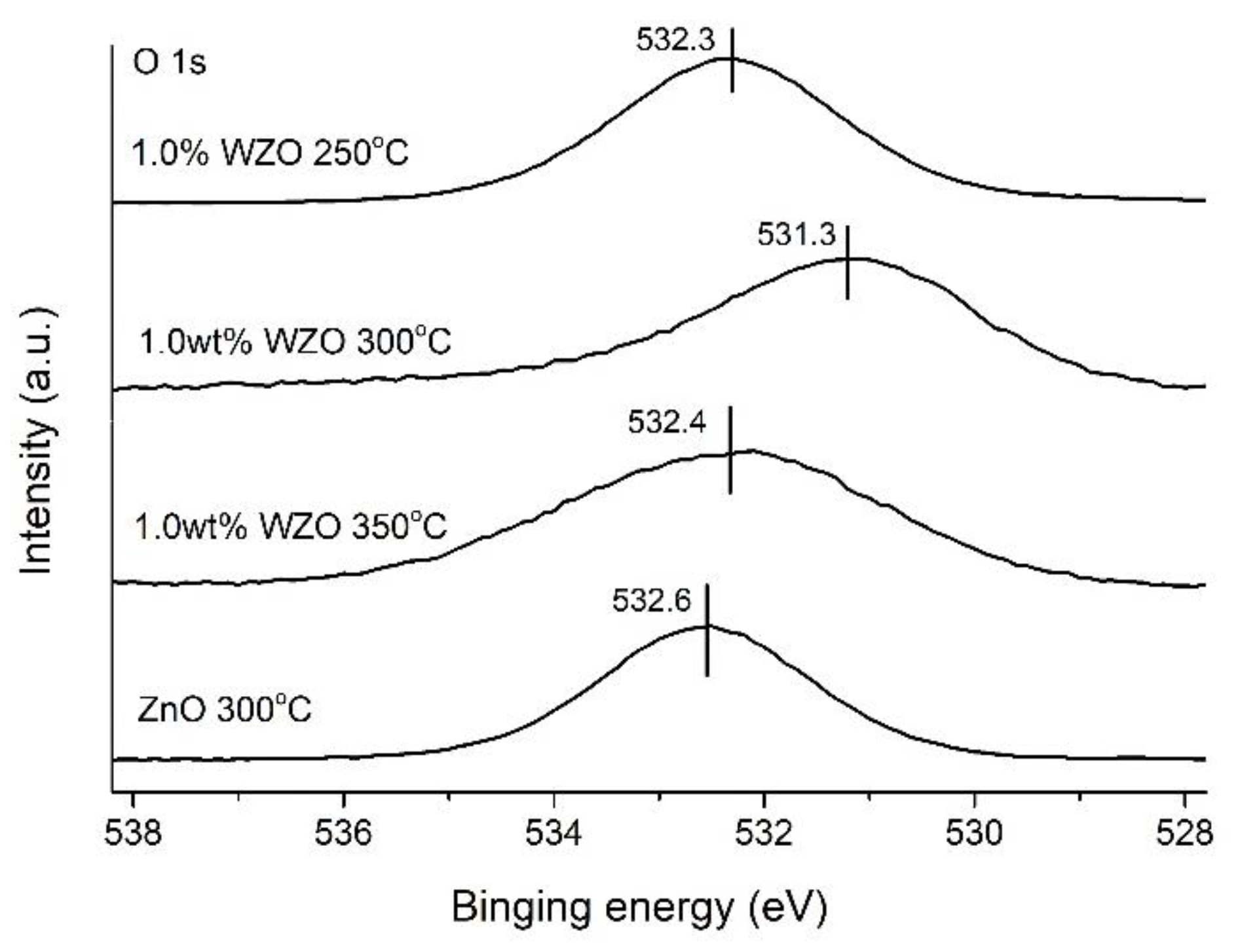
The O 1s XPS peaks of the ZnO film grown at 300 °C and 1.0 wt.% WZO films grown from 250 to 350 °C are presented in
Figure 13. The O 1s peak of the ZnO film was located at 532.6 eV, which was higher than those of the 3 WZO films (532.3, 531.3, and 532.4 eV). The appearance of the peak at a higher binding energy was ascribed to the presence of O
2- ions in the deficient regions within the ZnO matrix [
33]. Compared to the O 1s peak of the ZnO film, the core peaks of the other 3 WZO films were located in lower binding energies, which was theoretically attributed to the substitution of Zn with W atoms [
23].
Figure 14 shows the narrow-scanning XPS data for the peak intensities of Zn 2p1/2 and Zn 2p3/2 for the ZnO film grown at 300 °C and 1.0 wt.% WZO films grown at 250–350 °C. The core peaks of Zn 2p1/2 and Zn 2p3/2 for the ZnO film were located at 1045.4 and 1022.1 eV, respectively, surpassing those of the 3 WZO films. Notably, the Zn 2p1/2 core peaks tended to shift to higher binding energies as the growth temperature increased. This phenomenon was attributed to the loss of electrons from Zn
2+ ions while in their oxidised states, due to the increase in the growth temperature [
23,
33].
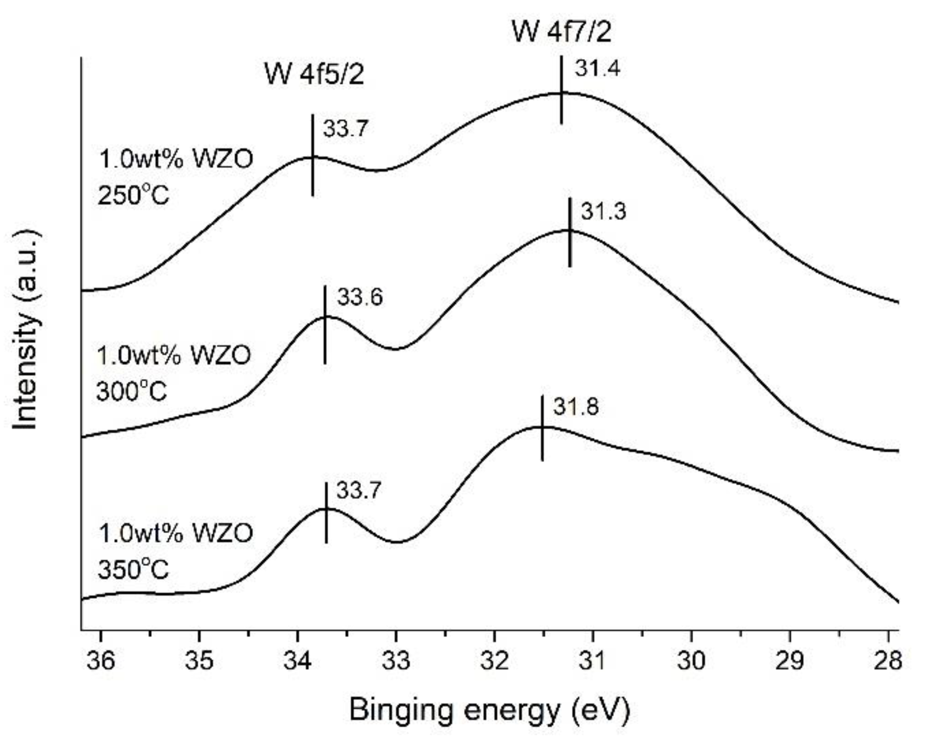
Figure 15 displays the narrow-scanning XPS data of the W 4f5/2 and W 4f7/2 peaks for the 1.0 wt.% WZO films grown at 250–350 °C. The W 4f5/2 peak appeared at 33.7, 33.6, and 33.7 eV, and was associated with the metallic and oxidation characteristics of the WZO films. Accordingly, the O 1s peak was located at approximately 531.3–532.6 eV, corresponding to the W=O bonds. The W 4f7/2 core peak, which is the feature peak of W metal, appeared at 31.4, 31.3, and 31.8 eV. This indicated that the fabricated WZO films preserved their W-metallic characteristics, as well as the formation of an oxide layer [
34,
35].
4. Conclusions
In this paper, 1.0 wt.% WZO films were successfully fabricated on glass substrates under different growth temperatures (200–400 °C) via a pulse laser deposition technique. Investigations on their electrical properties suggested that the 1.0 wt.% WZO film grown at 300 °C exhibited the lowest resistivity among all films (1.97 × 10⁻³ Ω-cm), as well as an excellent carrier mobility (9.27 cm2/V·s) and carrier concentration (3.42 × 1020 cm−3). The XRD results showed that all WZO films maintained the characteristics of the pristine ZnO film, while exhibiting a preferred orientation of crystallinity along the c-axis. The SEM images revealed the morphology of the WZO films, confirming their fine crystalline characteristics and smooth surface. The measured transparencies of the WZO films exceeded 75% in the 400–700 nm visible-light range. WZO films with different W-doping percentages (1.0–9.0 wt.%) were reviewed under a constant growth temperature (300 °C), and the results indicated that the carrier mobility tendency was inversely proportional to the W-doping percentage. Moreover, the surface elemental composition of the WZO and ZnO films for O, Zn, and W elements were verified by XPS analysis. In conclusion, our findings suggest that 1.0 wt.% WZO films grown at 300 °C could offer a promising platform for enhancing the transparency and conductivity of oxide materials used in optical and electrical devices.
Author Contributions
Formal analysis, P.-C.P.; investigation, P.-C.P.; methodology, P.-C.P. and H.-S.K.; project administration, C.-M.C.; visualization, D.-X.C.; writing—original draft, P.-C.P.; writing—review and editing, C.-M.C. and H.-S.K. All authors have read and agreed to the published version of the manuscript.
Funding
This research was funded by the Ministry of Science and Technology of Taiwan, grant number 110-2637-E-027-002.
Institutional Review Board Statement
Not applicable.
Informed Consent Statement
Not applicable.
Data Availability Statement
Not applicable.
Acknowledgments
The authors gratefully appreciate the technical support provided from Maw-Kuen Wu, the Distinguished Research Fellow of Academia Sinica.
Conflicts of Interest
The authors declare no conflict of interest.
References
- Wang, B.; Yu, F.; Li, H.; Song, T.; Nan, D.; He, L.; Duan, H.; Wang, S.; Tang, X. The preparation and photocatalytic properties of Na doped ZnO porous film composited with Ag nano-sheets. Phys. E Low-Dimens. Syst. Nanostruct. 2020, 117, 113712. [Google Scholar] [CrossRef]
- Sharmin, A.; Tabassum, S.; Bashar, M.S.; Mahmood, Z.H. Depositions and characterization of sol–gel processed Al-doped ZnO (AZO) as transparent conducting oxide (TCO) for solar cell application. J. Theor. Appl. Phys. 2019, 13, 123–132. [Google Scholar] [CrossRef] [Green Version]
- Shinagawa, T.; Shibata, K.; Shimomura, O.; Chigane, M.; Numura, R.; Izaki, M. Solution-processed high-haze ZnO pyramidal textures directly grown on a TCO substrate and the light-trapping effect in Cu2O solar cells. J. Mater. Chem. C 2014, 2, 2908–2917. [Google Scholar] [CrossRef]
- Ellmer, K. Resistivity of polycrystalline zinc oxide films: Current status and physical limit. J. Phys. D Appl. Phys. 2001, 34, 3097–3108. [Google Scholar] [CrossRef]
- Stojadinovic, S.; Vasilic, R.; Radic, N.; Tadic, N.; Stefanov, P.; Grbic, B. The formation of tungsten doped Al2O3/ZnO coatings on aluminum by plasma electrolytic oxidation and their application in photocatalysis. Appl. Surf. Sci. 2016, 377, 37–43. [Google Scholar] [CrossRef]
- Vijayalakshmi, K.; Renitta, A. Enhanced hydrogen sensing performance of tungsten activated ZnO nanorod arrays prepared on conductive ITO substrate. Ceram. Int. 2015, 41, 14315–14325. [Google Scholar] [CrossRef]
- Pawar, B.N.; Jadkar, S.R.; Takwale, M.G. Deposition and characterization of transparent and conductive sprayed ZnO:B thin films. J. Phys. Chem. Solids 2005, 66, 1779–1782. [Google Scholar] [CrossRef]
- Eskalen, H.; Kavun, Y.; Kerli, S.; Eken, S. An investigation of radiation shielding properties of boron doped ZnO thin films. Opt. Mater. 2020, 105, 109871. [Google Scholar] [CrossRef]
- Tsay, C.-Y.; Hsu, W.-T. Sol-gel derived undoped and boron-doped ZnO semiconductor thin films: Preparation and characterization. Ceram. Int. 2013, 39, 7425–7432. [Google Scholar] [CrossRef]
- Duygulu, N.E.; Kodolbas, A.O.; Ekerim, A. Effects of argon pressure and r.f. power on magnetron sputtered aluminum doped ZnO thin films. J. Cryst. Growth 2014, 394, 116–125. [Google Scholar] [CrossRef]
- Mamat, M.H.; Sahdan, M.Z.; Khusami, Z.; Ahmed, A.Z.; Abdulah, S.; Rusop, M. Influence of doping concentrations on the aluminum doped znic oxide thin films properties for ultraviolet photoconductive sensor applications. Opt. Mater. 2010, 32, 696–699. [Google Scholar] [CrossRef]
- Ito, N.; Sato, Y.; Song, P.K.; Kaijio, A.; Inoue, K.; Shigesato, Y. Electrical and optical properties of amorphous indium zinc oxide films. Thin Solid Film. 2006, 496, 99–103. [Google Scholar] [CrossRef]
- Gomez, H.; Maldonado, A.; de la L. Olvera, M.; Acosta, D.R. Gallium-doped ZnO thin films deposited by chemical spray. Sol. Energy Mater. Sol. Cells 2005, 87, 107–116. [Google Scholar] [CrossRef]
- Yu, C.-F.; Chen, S.-H.; Sun, S.-J.; Chou, H. Influence of the grain boundary barrier height on the electrical properties of Gallium doped ZnO thin films. Appl. Surf. Sci. 2011, 257, 6498–6502. [Google Scholar] [CrossRef]
- Yoon, H.S.; Lee, K.S.; Lee, T.S.; Cheong, B.; Choi, D.K.; Kim, D.H.; Kim, W.M. Properties of fluorine doped ZnO thin films deposited by magnetron sputtering. Sol. Energy Mater. Sol. Cells 2008, 92, 1366–1372. [Google Scholar] [CrossRef]
- Tsai, Y.-Z.; Wang, N.-F.; Tsai, C.-L. Fluorine-doped ZnO transparent conducting thin films prepared by radio frequency magnetron sputtering. Thin Solid Film. 2010, 518, 4955–4959. [Google Scholar] [CrossRef]
- Firooz, A.A.; Keyhani, M. The effect of different dopants (Cr, Mn, Fe, Co, Cu and Ni) on photocatalytic properties of ZnO nanostructures. Int. J. Nanosci. Nanotechnol. 2020, 16, 59–65. [Google Scholar]
- Ngom, B.D.; Mpahane, T.; Manyala, N.; Nemraoui, O.; Buttner, U.; Kana, J.B.; Fasasi, A.Y.; Maaza, M.; Bey, A.C. Structural and optical properties of nano-structured tungsten-doped ZnO thin films grown by pulsed laser deposition. Appl. Surf. Sci. 2009, 255, 4153–4158. [Google Scholar] [CrossRef]
- Zhang, H.F.; Liu, H.F.; Lei, C.X.; Yuan, C.K.; Zhou, A.P. Tungsten-doped ZnO transparent conducting films deposited by direct current magnetron sputtering. Vacuum 2010, 85, 184–186. [Google Scholar] [CrossRef]
- Chen, Y.C.; Hu, Y.H.; Zhang, X.H.; Hu, K.Y.; Tong, F.; Lao, Z.X.; Shuai, W.Q. Investigation of the propertie of W-doped ZnO thin films with modulation power deposition by RF magnetron sputtering. J. Mater. Sci. Mater. Electron. 2017, 28, 5498–5503. [Google Scholar] [CrossRef]
- Yang, H.L.; Xu, X.G.; Zhou, X.Y.; Ma, Y.N.; Dong, J.; Wang, T.Q.; Miao, J.; Jiang, Y. Dependence of ferromagnetric properties on growth oxygen partical pressure in boron-doped ZnO thin films. J. Mater. Sci. 2012, 47, 6513–6516. [Google Scholar] [CrossRef]
- Moafi, H.F.; Zanjanchi, M.A.; Shojaie, A.F. Tungsten-doped ZnO nanocomposite: Synthesis, characterization, and highly active photocatalyst toward dye photodegradation. Mater. Chem. Phys. 2013, 139, 856–864. [Google Scholar] [CrossRef]
- Sun, Y.-T.A.; Pan, P.-C.; Koo, H.-S.; Lin, N.-Y. Growth of low resistivity and high transparency boron-doped zinc oxide film by pulse laser deposition. Precis. Eng. 2020, 66, 605–610. [Google Scholar] [CrossRef]
- Zhang, C.; Chen, X.-L.; Chen, X.-H.; Tian, C.-S.; Huang, Q.; Zhao, Y.; Zhang, X.-D. Temperature-dependent growth and properties of W-doped ZnO thin films deposited by reactive magnetron sputtering. Appl. Surf. Sci. 2013, 274, 371–377. [Google Scholar] [CrossRef]
- Kumar, V.; Singh, R.G.; Purohit, L.P.; Mehra, R.M. Structural, Transport and optical properties of boron-doped zinc oxide nanocrystalline. J. Mater. Sci. Technol. 2011, 27, 481–488. [Google Scholar] [CrossRef]
- Mass, J.; Bhattacharya, P.; Katiyar, R.S. Effect of high substrate temperature on Al-doped ZnO thin films grown by pulsed laser deposition. Mater. Sci. Eng. 2003, B103, 9–15. [Google Scholar] [CrossRef]
- Lu, J.G.; Ye, Z.Z.; Zeng, Y.J.; Zhu, L.P.; Wang, L.; Yuan, J.B.; Zhao, H.; Liang, Q.L. Structural, optical, and electrical properties of (Zn,Al)O films over a wide range of compositions. J. Appl. Phys. 2006, 100, 073714. [Google Scholar] [CrossRef]
- Suo, X.X.; Zhao, S.J.; Ran, Y.J.; Liu, H.N.; Jiang, Z.T.; Li, Y.L.; Wang, Z. Effects of oxygen/argon pressure ratio on the structural and optical properties of Mn-doped ZnO thin films prepared by magnetron pulsed co-sputtering. Surf. Coat. Technol. 2019, 357, 978–983. [Google Scholar] [CrossRef]
- Mao, C.Y.; Fang, L.; Zhang, H.; Li, W.J.; Wu, F.; Qin, G.P.; Ruan, H.B.; Kong, C.Y. Effect of B doping on optical, electrical properties and defects of ZnO films. J. Alloys Compd. 2016, 676, 135–141. [Google Scholar] [CrossRef]
- Jun, M.-C.; Park, S.-U.; Koh, J.-H. Comparative studies of Al-doped ZnO and Ga-doped ZnO transparent conducting oxide thin films. Nanoscale Res. Lett. 2012, 7, 639–644. Available online: http://www.nanoscalereslett.com/content/7/1/639 (accessed on 22 November 2012). [CrossRef] [Green Version]
- Al-Gaashani, R.; Radiman, S.; Daud, A.R.; Tabet, N.; Al-Douri, Y. XPS and optical studies of different morphologies of ZnO nanostructures prepared by microwave methods. Cermics Int. 2013, 39, 2283–2292. [Google Scholar] [CrossRef]
- Greczynski, G.; Hultman, L. C 1s Peak of Adventitious Carbon Aligns to the Vacuum Level: Dire Consequences for Material’s Bonding Assignment by Photoelectron Spectroscopy. ChemPhysChem 2017, 18, 1507–1512. [Google Scholar] [CrossRef] [PubMed]
- Morozov, I.G.; Belousova, O.V.; Ortega, D.; Mafina, M.-K.; Kuznetcov, M.V. Structural, optical, XPS and magnetic properties of Zn particles capped by ZnO nanoparticles. J. Alloys Compd. 2015, 633, 237–245. [Google Scholar] [CrossRef]
- Spanu, D.; Recchia, S.; Schmuki, P.; Altomare, M. Thermal-oxidative growth of substoichiometric WO3–x nanowires at mild conditions. Phys. Status Soildi RRL 2020, 14, 2000235. [Google Scholar] [CrossRef]
- Charton, P.; Gengembre, L.; Armand, P. TeO2-WO3 glasses: Infrared, XPS and XANES structural characterizations. J. Solid-State Chem. 2002, 168, 175–183. [Google Scholar] [CrossRef]
Figure 1.
XRD patterns of pure ZnO and 1.0 wt.% WZO targets.
Figure 1.
XRD patterns of pure ZnO and 1.0 wt.% WZO targets.
Figure 2.
XRD patterns of WZO films deposited under different growth temperatures (200–400 °C).
Figure 2.
XRD patterns of WZO films deposited under different growth temperatures (200–400 °C).
Figure 3.
2θ angle of (002) diffraction peak of WZO films as a function of different growth temperatures (from 200 to 400 °C).
Figure 3.
2θ angle of (002) diffraction peak of WZO films as a function of different growth temperatures (from 200 to 400 °C).
Figure 4.
Grain size distribution and FWHM variation of the 1.0 wt.% WZO films grown at 200–400 °C.
Figure 4.
Grain size distribution and FWHM variation of the 1.0 wt.% WZO films grown at 200–400 °C.
Figure 5.
SEM images of 1.0 wt.% WZO films deposited at: (a) 200 °C, (b) 250 °C, (c) 300 °C, (d) 350 °C, and (e) 400 °C. (f) Pure ZnO film deposited at 300 °C. (g) Cross-sectional view of 1.0 wt.% WZO film deposited at 300 °C.
Figure 5.
SEM images of 1.0 wt.% WZO films deposited at: (a) 200 °C, (b) 250 °C, (c) 300 °C, (d) 350 °C, and (e) 400 °C. (f) Pure ZnO film deposited at 300 °C. (g) Cross-sectional view of 1.0 wt.% WZO film deposited at 300 °C.
Figure 6.
Electrical properties of 1.0 wt.% WZO films deposited at 200–400 °C.
Figure 6.
Electrical properties of 1.0 wt.% WZO films deposited at 200–400 °C.
Figure 7.
Electrical properties of 1.0, 3.0, 5.0, 7.0, and 9.0 wt.% WZO films deposited at 300 °C.
Figure 7.
Electrical properties of 1.0, 3.0, 5.0, 7.0, and 9.0 wt.% WZO films deposited at 300 °C.
Figure 8.
Optical properties of 1.0 wt.% WZO films deposited under 200–400 °C.
Figure 8.
Optical properties of 1.0 wt.% WZO films deposited under 200–400 °C.
Figure 9.
(a) Bandgaps of 1.0 wt.% WZO films deposited under different growth temperatures (200–400 °C). (b) Bandgap comparison between ZnO and 1.0 wt.% WZO films grown at 300 °C.
Figure 9.
(a) Bandgaps of 1.0 wt.% WZO films deposited under different growth temperatures (200–400 °C). (b) Bandgap comparison between ZnO and 1.0 wt.% WZO films grown at 300 °C.
Figure 10.
PL spectra in the 343–371 nm wavelength range of the 1.0 wt.% WZO films grown at 200–400 °C.
Figure 10.
PL spectra in the 343–371 nm wavelength range of the 1.0 wt.% WZO films grown at 200–400 °C.
Figure 11.
Full-length XPS spectra of ZnO and 1.0 wt.% WZO films grown at 300 °C.
Figure 11.
Full-length XPS spectra of ZnO and 1.0 wt.% WZO films grown at 300 °C.
Figure 12.
C 1s peak intensity of 1.0 wt.% WZO films grown at (a) 250 °C, (b) 300 °C, (c) 350 °C, and (d) ZnO film grown at 300 °C.
Figure 12.
C 1s peak intensity of 1.0 wt.% WZO films grown at (a) 250 °C, (b) 300 °C, (c) 350 °C, and (d) ZnO film grown at 300 °C.
Figure 13.
O 1s peak intensities of 1.0 wt.% WZO films grown at 250–350 °C and ZnO film grown at 300 °C.
Figure 13.
O 1s peak intensities of 1.0 wt.% WZO films grown at 250–350 °C and ZnO film grown at 300 °C.
Figure 14.
Zn 2p1/2 and Zn 2p3/2 peak intensities of 1.0 wt.% WZO films grown at 250 °C, 300 °C, and 350 °C, and ZnO film grown at 300 °C.
Figure 14.
Zn 2p1/2 and Zn 2p3/2 peak intensities of 1.0 wt.% WZO films grown at 250 °C, 300 °C, and 350 °C, and ZnO film grown at 300 °C.
Figure 15.
W 4f5/2 and W 4f/2 peak intensities of 1.0 wt.% WZO films grown at 250 °C, 300 °C, and 350 °C.
Figure 15.
W 4f5/2 and W 4f/2 peak intensities of 1.0 wt.% WZO films grown at 250 °C, 300 °C, and 350 °C.
Table 1.
Comparison of electrical properties between pure ZnO and 1.0 wt.% WZO films deposited at 300 °C.
Table 1.
Comparison of electrical properties between pure ZnO and 1.0 wt.% WZO films deposited at 300 °C.
| Film Type | Resistivity
(Ω-cm) | Carrier Mobility
(cm2/V·s) | Carrier Concentration
(1020/cm3) |
|---|
| ZnO | 3.87 × 10⁻³ | 6.65 | 2.43 |
| 1.0 wt.% WZO | 1.97 × 10⁻³ | 9.27 | 3.42 |
Table 2.
Transparencies of 1.0 wt.% WZO films deposited under different growth temperatures (200–400 °C) at the wavelengths of 460, 550, and 700 nm.
Table 2.
Transparencies of 1.0 wt.% WZO films deposited under different growth temperatures (200–400 °C) at the wavelengths of 460, 550, and 700 nm.
| Growth Temperature | 460 nm | 550 nm | 700 nm |
|---|
| 200 °C | 76.51% | 76.96% | 78.71% |
| 250 °C | 76.08% | 77.51% | 80.17% |
| 300 °C | 77.12% | 78.01% | 80.49% |
| 350 °C | 80.08% | 83.14% | 85.92% |
| 400 °C | 81.20% | 83.99% | 86.44% |
| Publisher’s Note: MDPI stays neutral with regard to jurisdictional claims in published maps and institutional affiliations. |
© 2022 by the authors. Licensee MDPI, Basel, Switzerland. This article is an open access article distributed under the terms and conditions of the Creative Commons Attribution (CC BY) license (https://creativecommons.org/licenses/by/4.0/).


