Article

Narrowband Near-Infrared Perovskite/Organic Photodetector: TCAD Numerical Simulation

by
Marwa S. Salem
1,2,
Ahmed Shaker
3,*,
Amal H. Al-Bagawia
4,
Ghada Mohamed Aleid
5,
Mohamed S. Othman
5,
Mohammad T. Alshammari
6 and
Mostafa Fedawy
7,8
1
Department of Computer Engineering, College of Computer Science and Engineering, University of Ha’il, Hail 55211, Saudi Arabia
2
Department of Electrical Communication and Electronics Systems Engineering, Faculty of Engineering, Modern Science and Arts University (MSA), Cairo 12556, Egypt
3
Engineering Physics and Mathematics Department, Faculty of Engineering, Ain Shams University, Cairo 11566, Egypt
4
Chemistry Department, Faculty of Science, University of Ha’il, Hail 55211, Saudi Arabia
5
B.Sc. Department, Preparatory Year College, University of Ha’il, Hail 55211, Saudi Arabia
6
Department of Computer Science and Information, Computer Science and Engineering College, University of Ha’il, Hail 55211, Saudi Arabia
7
Electronics and Communications Department, Faculty of Engineering, Arab Academy for Science and Technology and Maritime Transport, Cairo 11736, Egypt
8
Center of Excellence in Nanotechnology, Arab Academy for Science and Technology and Maritime Transport, Cairo 11736, Egypt
*
Author to whom correspondence should be addressed.
Crystals 2022, 12(8), 1033; https://doi.org/10.3390/cryst12081033
Submission received: 6 July 2022 / Revised: 21 July 2022 / Accepted: 21 July 2022 / Published: 25 July 2022

Abstract

:
Narrowband photodetectors (PD) established in the near-infrared (NIR) wavelength range are highly required in a variety of applications including high-quality bioimaging. In this simulation study, we propose a filter-less narrowband PD based on the architecture of perovskite/organic heterojunction. The most decisive part of the photodetector is the hierarchical configuration of a larger bandgap perovskite material with a thicker film followed by a lower bandgap organic material with a narrower layer. The design of the structure is carried out by TCAD numerical simulations. Our structure is based on an experimentally validated wideband organic PD, which is modified by invoking an additional perovskite layer having a tunable bandgap. The main detector device comprises of ITO/perovskite (CsyFA1−yPb(IxBr1−x)3)/organic blend (PBDTTT-c:C60-PCBM)/PEDOT:PSS/Al. The simulation results show that the proposed heterojunction PD achieves satisfactory performance when the thickness of perovskite and organic layers are 2.5 µm and 500 nm, respectively. The designed photodetector achieves a narrow spectral response at 730 nm with a full width at half-maximum (FWHM) of 33 nm in the detector, while having a responsivity of about 0.12 A/W at zero bias. The presented heterojunction perovskite/organic PD can efficiently detect light in the wavelength range of 700 to 900 nm. These simulation results can be employed to drive the development of filter-less narrowband NIR heterojunction PD.

1. Introduction

Narrowband photodetectors (PDs) have been broadly utilized in various application fields like biomedical imaging, virtual reality, navigation aid, full-weather robots, and many others [1,2,3,4,5]. In these PDs, light can be detected inside a specific wavelength range, and there is no light response at other wavelengths. The existing commercial market of PDs is dominated by expensive crystalline inorganic semiconductor structures, which are usually integrated with optical filters [6]. Meanwhile, organic semiconductors can compete the existing technologies because they are lightweight and flexible besides their low-cost and semi-transparent nature. In addition, organic materials have high absorption coefficients and can effectively be designed as absorber materials at thickness lower than only 1 µm. Additionally, the absorption spectrum of organic materials can be modulated by modifying their molecular configurations. These promising features make organic PDs prospective contenders for the expanding need for smarter and safer detectors [7,8,9].
Most organic PDs are composed of a blend of a polymer donor and fullerene acceptor molecules as the photoactive thin film [10]. Although broadband organic PDs can be commonly attained [11,12,13], it is not that easy to achieve narrowband organic PDs due to the relatively wide photon harvesting range of organic semiconductors [14,15]. Moreover, organic–inorganic hybrid perovskite materials are developing candidates that have been extensively used in PDs [16]. Some of the advantages of perovskites are their pronouncing optical and electrical properties, involving a direct bandgap, large extinction coefficient, and high carrier mobility [17,18]. It has been shown that by combining organic–inorganic hybrid perovskites and an organic heterojunction comprising of donor–acceptor materials can push this type of PDs to cover the near-infrared range resulting in broadband PDs [19,20]. A hybrid PD with perovskite/polymer, which is based on CH3NH3PbI3-xBrx/PTB7 with tunable spectral response in the range 680–710 nm, has been reported [21]. Furthermore, it has been demonstrated that a hybrid PD with perovskite/polymer heterojunction based on CH3NH3PbI3/PCPDTBT:PC71BM can achieve a visible-blind narrowband NIR detection [22].
Notably, the biological tissues are primarily comprised of hemoglobin and water that absorb wavelengths below 650 nm and above 900 nm [23]. Consequently, in order to prevent the light absorption of biological tissue, a PD operating in the range 650 to 900 nm is required [24]. Therefore, our aim in this work is to design a narrowband PD that is based on perovskite/organic heterojunction to provide an optimal detection region. The design idea is based on selecting a relatively wide band gap perovskite that can fully absorb the incident photons whose wavelengths are smaller than the perovskite cutoff wavelength [25]. This can be accomplished if the perovskite layer has a wider thickness and higher defect density than the organic layer [26]. When the light passes through the perovskite, the visible light is absorbed while the NIR light will be transferred to the organic layer due to the transparency of the perovskite layer in the NIR region. So, the organic material will respond to the light spectrum between the cutoff wavelengths corresponding to the organic and perovskite materials. Next, the photoexcited charge carriers in the organic layer will be separated by the produced built-in electric field, which is a process that is nearly not impacted by the defects in the organic film. This perovskite/organic PD design does not require a complex filtering system and may operate under zero bias due to the presence of a built-in electric field at the heterojunction. So, it can be used as a filter-free and self-powered device.
In order to design and reveal the internal physics of an optoelectronic device, a TCAD simulation meticulously addressing the basic optical, electrical, and semiconductor characteristics is enormously valuable. Such an advanced simulation can accomplish an accurate performance evaluation of various PDs and provide exact physical pictures that reflect the detailed device operation. Compared to the complex and time-consuming experiments, a highly effective and precise simulation can be extremely beneficial for predicting and optimizing the device performance in a convenient way. In this work, numerical simulations were carried out using Silvaco TCAD device simulator package [27]. We performed finite element simulations enabling electro-optical modeling of our proposed PD. Currently, such a simulation of narrowband perovskite/organic PD has never been reported.
This work thus focuses on the design and numerical analysis of a narrowband perovskite/organic PD. The selected perovskite material is CsyFA1−yPb(IxBr1−x)3 whose bandgap can be tuned in the range 1.5 to 1.8 eV [28]. Meanwhile, the organic material is a blend between the donor polymer PBDTTT-c and the acceptor C60-PCBM. This organic material has a band gap of about 1.45 eV, and PDs based on this organic semiconductor have been experimentally validated as wideband PDs [29]. Thus, a calibration step will be presented to confirm the physical and geometrical parameters used in simulation by comparing the TCAD simulation results versus the experimental data [29]. Then, we will study the impact of the energy gap of the perovskite material to get the optimum choice based on responsivity (R) and full width at half-maximum (FHWM) parameters. Moreover, the impact of reverse bias and organic thickness and trap density is investigated.

2. Simulation Methodology and Device Model

To build our structure model and simulate the electrical and optical characteristics of the proposed PD, the Silvaco TCAD device simulator module is utilized. The involved numerical simulation is based on the discretized solution of the basic equations of charge transport in semiconductors like Poisson’s equation, continuity, and transport equations. Firstly, given an illuminated input source, the optical intensity profiles within the PD device are calculated. Then, the intensity profiles are transformed into photogeneration rates, which are integrated into the generation terms in the continuity equations. In optoelectronic device simulation, two separate models are computed concurrently at each bias. These models are the optical ray tracing and the photogeneration model. In the first model, the real component of the refractive index is adopted to evaluate the optical intensity, while, in the second model, the extinction coefficient is employed in the calculation of a new carrier concentration. An electrical simulation is then accomplished to acquire the required terminal currents [30], where the drift diffusion model is employed to simulate the transport properties. The physical models used in simulation are as follows. The Shockley–Read–Hall (SRH) recombination model and Poole–Frenkel mobility model were enabled. Notably, the SRH recombination mechanism arises from the recombination of electron–hole pairs through defect levels within the energy bandgap of the simulated material [31,32].

2.1. Basic Photodetector Structure

The schematic diagram of the proposed detector is displayed in Figure 1a. In the simulation process, the perovskite/organic heterojunction PD structure was generated by the device simulator on a 2D grid as displayed in Figure 2b. The corresponding energy levels of the distinct layers are displayed in Figure 1c, while the energy band diagram at dark condition is plotted in Figure 1d. As depicted in the schematic figure, the basic structure of the PD is ITO/PEIE followed by CsyFA1−yPb(IxBr1−x)3. This perovskite material was chosen because it is more stable than MA-based compounds [33] and due to its bandgap tunability [28]. Thus, CsyFA1−yPbIxBr(1−x)3 can serve as a suitable partner in the heterojunction detector combining with a proper organic material. Light is incident from the ITO side and passes through the perovskite film where photons of wavelengths smaller than a certain designed wavelength are suppressed (see Figure 1c). The active organic film is PBDTTT-c:C60-PCBM (donor/acceptor). The thickness of the perovskite and organic layers is set as 2.5 μm and 500 nm, respectively. The hole transport layer (HTL) is PEDOT:PSS with a p-doping of about 1 × 1018 cm−3.
A summary of the technological and physical parameters of the PD layers is presented in Table 1 [28,29,34,35,36,37,38,39]. Further, Table 2 lists the main defect parameters inside the perovskite and organic blend layers [24,29]. The details and criteria of choosing these parameters are explained hereafter. Moreover, the refractive indices and distinction coefficients, which are extracted from experimental reports, are displayed in the Supplementary Materials [28,29,37]. It should be pointed out here that our proposed PD structure is based on a fabricated wideband organic PD. The modification made here is to add a thick perovskite layer in order to engineer the band of detection. Before proceeding to present our PD results, a validation of the parameters of the materials used in our PD design is conducted. This is done by comparing TCAD simulation results with those obtained from measurements of the fabricated organic PD [29]. The Silvaco script of this part is listed in the Supplementary Materials.

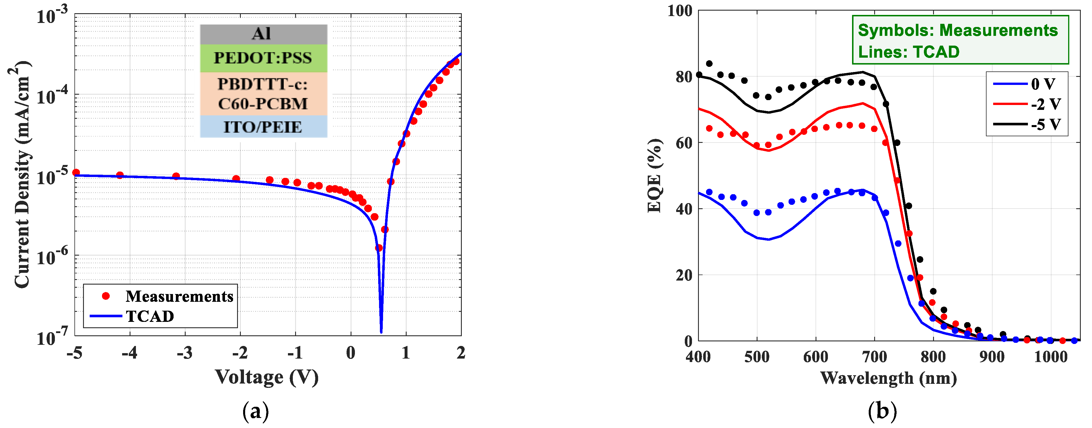
2.2. Calibration of the Fabricated Wideband Organic PD

The experimental device, used in calibration, consists of multiple layers stacked as shown in the inset of Figure 2a. The transparent conductive oxide is ITO/Polyethylenimide (PEIE), which is utilized to reduce the overall work function. The thickness of ITO/PEIE is 110 nm and is followed by the active layer. The active layer is PBDTTT-c (as donor material) and C60-PCBM (as acceptor material) with a 1:1.5 ratio in weight, and its thickness is 500 ± 20 nm. PEDOT:PSS, as HTL, is deposited on top of the active layer. The last deposited layer is aluminum, whose thickness is 100 nm. The work functions of ITO/PEIE and PEDOT:PSS are 4.2 and 4.9 eV, respectively, as determined by Kelvin probe [29]. The optical parameters of the distinct layers, namely, the refractive index and extinction coefficient, are taken from [39]. Regarding the active material physical parameters, they are extracted from the literature [29,38]. The LUMO and HOMO levels are 3.7 and 5.15 eV, respectively, giving a blend bandgap of 1.45 eV. Further, the electron and hole mobility is taken as 6 × 10⁻⁴ and 1 × 10⁻³ cm2/V.s, respectively [38]. Regarding the bulk trap defects, a donor trap density is estimated to be 2.7 × 1016 cm−3 at a position of 290 meV above the blend HOMO, while a trap density of 2 × 1014 cm−3 of a mid-gap trap state is fitted [39].
Figure 2a shows the current density vs. voltage of this wideband detector that was measured under 530 nm LED light having an intensity of 0.3 W/m2. The figure also shows the TCAD simulation results, which are fitted by adjusting the conduction and valence density of states and trap densities. More details about the calibration are found in [29,39]. Furthermore, Figure 2b exhibits the EQE characteristics under different bias conditions for the experimental and simulation results. The good agreement between the simulation results and those from measurements indicates a satisfactory validation of the material parameters and physical models applied in the simulator.

3. Results and Discussions

In this section, the TCAD simulation results of our proposed perovskite/organic material system PD are presented. The influence of trap density and thickness of the perovskite film is studied to get a design guideline about the main parameters of the perovskite layer that assure a narrowband detector operation. Next, the effect of the variation of the perovskite energy gap is explored. Finally, the impact of reverse bias on the PD main parameters is investigated. The key factors of the PD under study are extracted from the simulator once the simulation process is done. Besides the dark and illuminated output current, other parameters like responsivity (R) and full width at half maximum (FWHM) are considered significant metrics that can measure the effectiveness of the detector and also can be used to differentiate between different types of PDs. The responsivity of a PD is the ratio of the output photocurrent to the incident light power. It can be related to EQE as [23]:
R = EQE q λ h c
The FWHM is an important figure of merit for the narrowband PD as it defines the specificity of the detection wavelength as well as the imaging resolution.

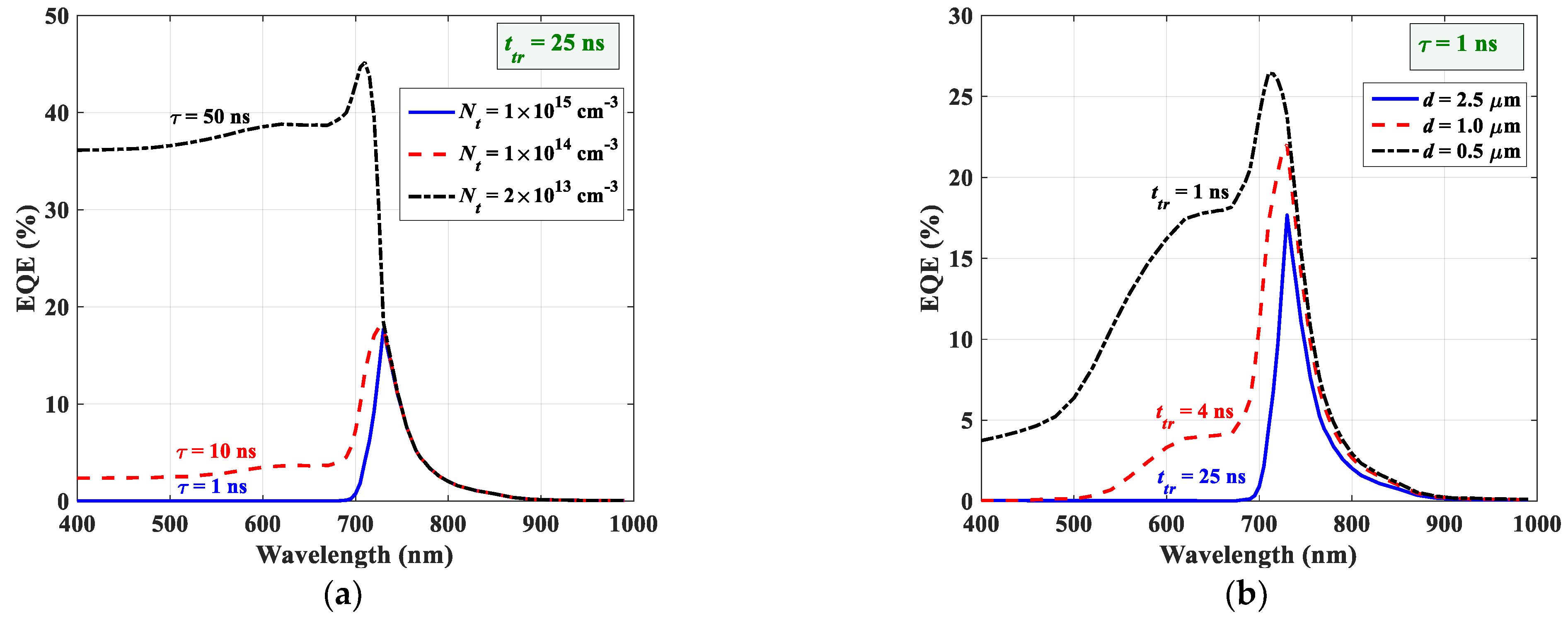
3.1. Impact of Trap Density and Thickness of Perovskite Layer

First, we test the impact of trap density (Nt) and thickness (d) of the perovskite film as the carrier lifetime, and thickness of the perovskite layer have to be designed carefully. This step is essential to check and ensure the design criterion of suppression of short wavelength range. In these simulations, the energy gap of the perovskite is set at 1.62 eV. All other parameters are fixed as in Table 1 and Table 2 unless otherwise stated. In this regard, the simulated external quantum efficiency (EQE) curves under 0 V bias are shown for different Nt and d values in Figure 3a and 3b, respectively. Upon decreasing Nt, the carrier lifetime (τ) increases. On the other hand, as long as d is constant, the transition time (ttr) is constant, which is given by,
t t r = d 2 μ V
where μ is the carrier mobility and V is the average electric potential along the perovskite layer. The calculated value of ttr is about 25 ns at d = 2.5 µm as shown in Figure 3a. When the transition time is much longer than the carrier lifetime, the photogenerated carriers recombine before collection occurs. This can be seen for higher values of Nt. However, when Nt is declined (down to 1 × 1013 cm−3), the transition time becomes lower than the carrier lifetime implying lower recombination probability, which results in higher EQE [23]. That is why it is crucial to keep high defect density in the perovskite film for an appropriate narrowband PD design. Moreover, the thickness of perovskite film is varied while keeping a fixed Nt = 1 × 1015 cm−3 (and so a fixed τ = 1 ns). The results show that when decreasing d, the transition time will drop as shown in Figure 3b. Once the transition time becomes comparable to the carrier lifetime, the carrier recombination likelihood decreases before the collection resulting in an increased EQE at the short wavelength. So, a thickness of perovskite film larger than 2 µm could be suitable to achieve an adequate narrowband PD operation.
To present more physical insight into the photo response of the PD in accordance with wavelength variation, we draw the profiles of the normalized photon absorption rate in two different cases as shown in Figure 4. The first case is for a perovskite thickness d = 2.5 µm, while the other one is for a thinner perovskite layer for which d = 0.5 µm. For the two cases, Nt = 1 × 1015 cm−3. As it can be inferred from Figure 4a, the distribution of photon absorption reveals that the part of incident light with wavelengths range shorter than about 700 nm can be completely absorbed primarily by the perovskite film. This results in the dominance of generation and recombination inside the perovskite and translates into low EQE below 700 nm, as indicated in Figure 3a. The fringes that originate from the interference progressively become noticeable for wavelengths longer than 700 nm up to about 850 nm. This means that the generation and recombination occur mainly inside the organic film, implying less absorption in the perovskite layer at higher wavelengths, which results in higher EQE. On the other hand, for thin perovskite film, the profile of the normalized photon absorption, displayed in Figure 4b, reveals that there is a penetration of photons in the organic layer for the wavelength range from 500 nm up to 700 nm. This result is supported by the behavior of the EQE shown in Figure 3b.

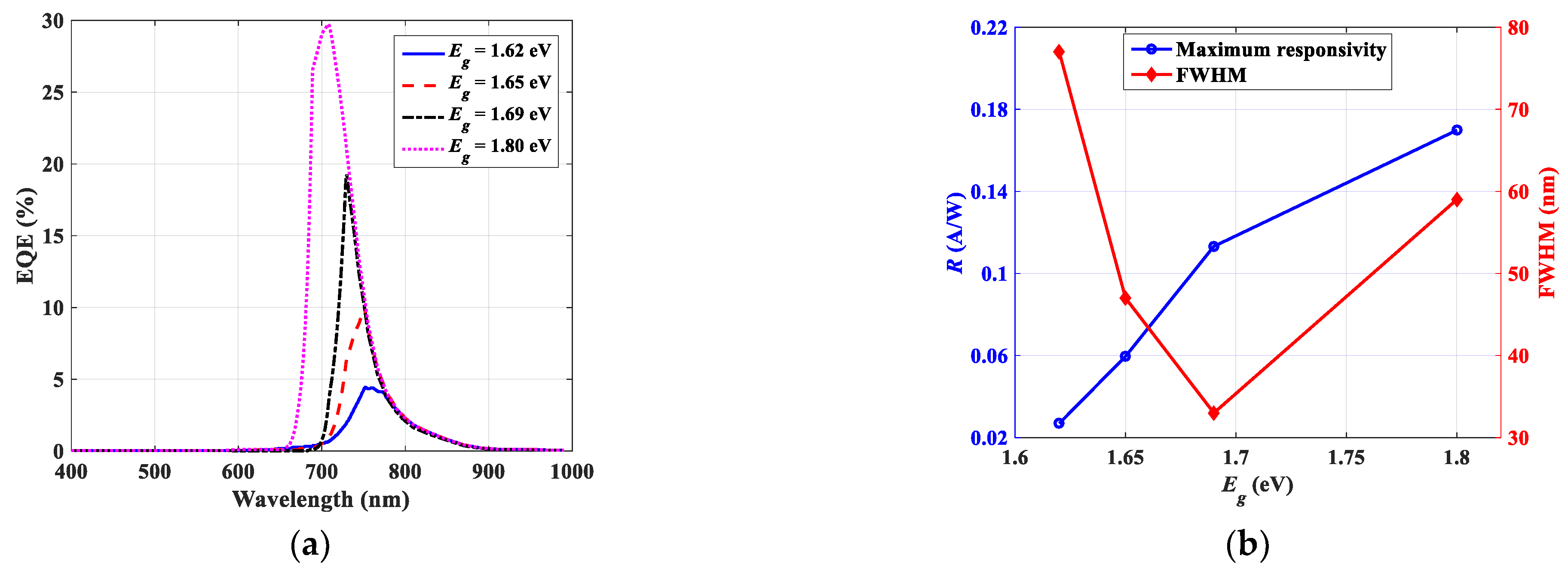
3.2. Impact of Energy Gap of Perovskite Material

As mentioned herein, CsyFA1−yPb(IxBr1−x)3 perovskite material is selected thanks to its bandgap tunability. In the following analysis, the impact of the energy gap of CsyFA1−yPb(IxBr1−x)3 on the photoresponsivity is examined. Figure 5a shows the EQE curves for different values of Eg. As Eg increases, the EQE increases as well; however, the FWHM increases, which means a broader band. For a quantitative difference between the various bandgap cases, we draw the peak responsivity and FWHM as seen in Figure 5b. It can be observed that the peak responsivity increases upon increasing Eg while there is an optimum minimum value of 33 nm that occurs at Eg = 1.69 eV. So, a suitable design can be chosen for which the energy gap of the perovskite layer is 1.69 eV. For this case, the peak responsivity is 0.12 A/W at a full width at half maximum of 33 nm.

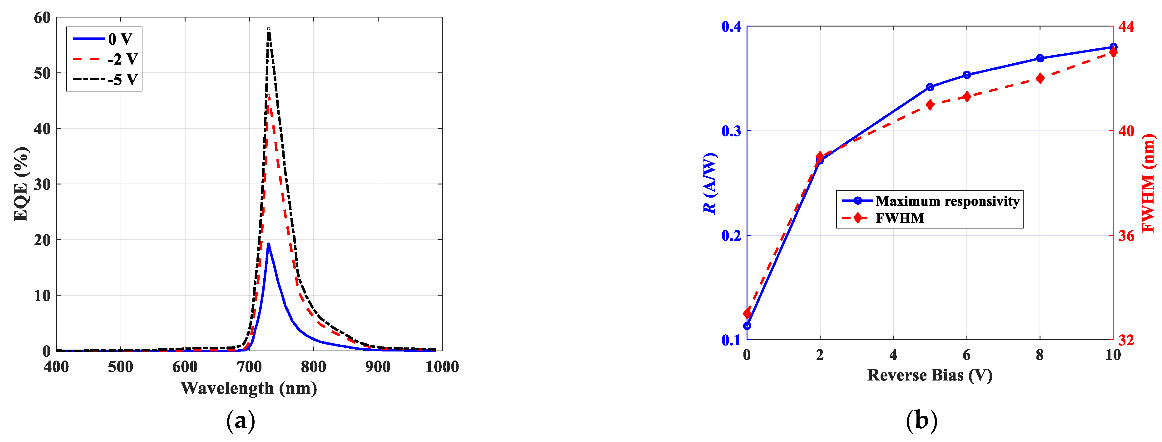
3.3. Impact of Reverse Bias

In this subsection, the influence of reverse bias on the PD performance is presented. In these simulations, the perovskite energy gap is taken to be 1.69 eV. Figure 6a displays the EQE for three cases of reverse bias at 0, 2, and 5 V. As the reverse bias rises, the EQE increases but the spectrum becomes wider. For a quantitative view on the biasing conditions, the peak responsivity and FWHM are plotted as shown in Figure 6b. As the reverse bias increases, the two PD parameters raise; however, the rate of rise is slowed. A suitable design could be achieved for a powered PD at a reverse voltage of 5 V. In this case, the peak responsivity and the FWHM are about 0.34 A/W and 41 nm, respectively.

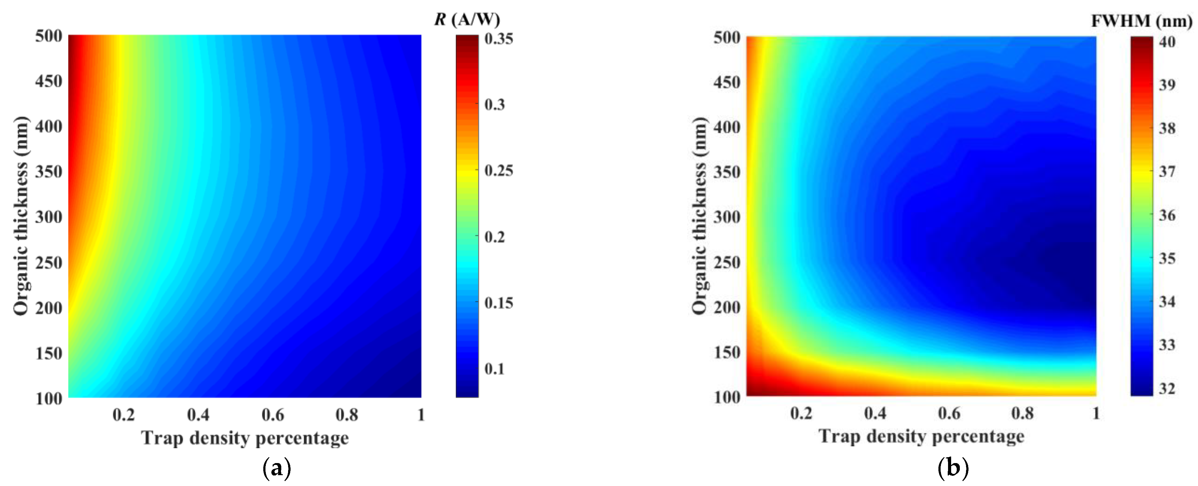
3.4. Impact of Organic Layer Thickness and Defects

Here, we provide a parametric study to examine the variation of the thickness and trap density of the organic layer on the responsivity and FWHM. The thickness is varied from 100 to 500 nm while the trap density is weighted by a factor from 5% to 100%. As seen in Figure 7, when the trap density declines, the responsivity increases (see Figure 7a); however, the FWHM trend is different (see Figure 7b). The FWHM is maximum for lower values of thickness given a fixed trap density. It is obvious that if the design thickness is at 500 nm, an optimum choice could be met for lower trap density. For a selected case of 10% reduction of the trap densities listed in Table 2, the responsivity is 0.3 A/W and the FWHM is 37 nm. Although the FWHM has increased by about 12% of the corresponding value at zero bias, an enhancement of 170% in R is achieved. This result shows the importance of decreasing the bulk defects in organic layers. With the continuous advancement in processing techniques, organic semiconductors can be enabled to have lower trap density and improved crystallinity.
Finally, a comparison between the key detector parameters of our structure and those of some organic and inorganic narrowband PDs is provided in Table 3. The PDs are divided into groups where the first group regards organic-base PDs showing structures of narrow band [40,41] and some others with a higher detection band [42,43]. Although the bias increases R and EQE, it results in widening the band [43]. The second category considers the hybrid perovskite/organic based PDs showing lower responsivity in comparison to organic candidates [21,22]. This is due to the thick perovskite layer, which generally reduces the photogeneration inside the organic film. In our hybrid system, the simulation results are encouraging as the value of R is comparable to organic PD while the FWHM is very narrow. The influence of bias is to increase R and FWHM besides it causes a redshift in the detection peak wavelength (λpeak). Moreover, reducing organic bulk defects results in a substantial rise in R, while the FWHM does not significantly degrade as evident from the results listed in Table 3.
Regarding inorganic PD candidates, a recent research study revealed a responsivity is 0.09 A/W with a FWHM of 35.3 nm at a peak wavelength of 735 nm for the CdSe/Sb2(S1−x,Sex)3 inorganic system [24]. Thus, compared to our results, the proposed perovskite/organic PD is promising and, upon appropriate design and simulation-driven experimental studies, could compete the inorganic system PDs.

4. Conclusions

In this paper, we report on the results of our simulation studies on the perovskite/organic heterojunction photodetector. A model structure of perovskite/organic heterojunction PD was built in Silvaco TCAD environment. The effects of perovskite layer thickness, trap density, and energy gap on the performance of the proposed PD are discussed. The simulations are conducted regarding the external quantum efficiency (EQE) curves. Besides, the main performance parameters like responsivity and full width at half maximum are also presented. The simulation results show that the proposed PD reveals optimum performance when the thickness of perovskite and organic layers are 2.5 µm and 500 nm, respectively. The FWHM has a minimum value of 33 nm at an energy gap of 1.69 eV of the perovskite material. The effect of reverse bias is also demonstrated, showing that a proper design could be accomplished for a powered PD at a reverse voltage of 5 V. Under this condition, the peak responsivity and the FWHM are about 0.34 A/W and 41 nm, respectively. Reducing the bulk trap density inside the organic has a positive effect, as R is substantially increased while the FWHM degrades by only 12%. This TCAD simulation study shows promising results and reveals that the design of perovskite/organic PD could be feasible. Additionally, the design concepts, presented in this paper, could be easily extended to other perovskite and organic partner materials.

Supplementary Materials

The following supporting information can be downloaded at: https://www.mdpi.com/article/10.3390/cryst12081033/s1, Figure S1: Optical constants (n and k) of (a) ITO and (b) PEDOT:PSS; Figure S2: Optical constants (n and k) of organic blend PBDTTT-c:C60-PCBM; Figure S3: Optical constants (n and k) of CsyFA1−yPb(IxBr1−x)3 by Ellipsometric measurements for (a) Eg = 1.62 eV, (b) Eg = 1.65, (c) Eg = 1.69 eV, and (d) Eg = 1.8 eV; Figure S4: Silvaco Script used to calibrate the wideband organic PD.

Author Contributions

Conceptualization, M.S.S., A.S. and M.T.A.; formal analysis, A.H.A.-B., G.M.A. and M.S.O.; software, M.S.S., A.S. and M.T.A.; investigation, M.S.S., A.S. and M.S.O.; methodology, M.S.S., M.T.A. and M.F.; supervision, A.S., A.H.A.-B. and M.T.A.; validation, M.S.S., G.M.A., A.H.A.-B. and M.F.; writing—original draft, M.S.S., A.H.A.-B. and G.M.A.; writing—review and editing, M.S.S., A.S. and M.S.O. All authors have read and agreed to the published version of the manuscript.

Funding

This research has been funded by Scientific Research Deanship at University of Ha’il–Saudi Arabia through project number RG-21 094.

Data Availability Statement

Not applicable.

Acknowledgments

The authors would like to express their great appreciation to Julie Euvrard for providing the experimental optical constants of the organic blend material used in our study.

Conflicts of Interest

The authors declare no conflict of interest.

References

  1. Wang, Y.; Kublitski, J.; Xing, S.; Dollinger, F.; Spoltore, D.; Benduhn, J.; Leo, K. Narrowband organic photodetectors–towards miniaturized, spectroscopic sensing. Mater. Horiz. 2022, 9, 220–251. [Google Scholar] [CrossRef] [PubMed]
  2. Wu, Y.L.; Fukuda, K.; Yokota, T.; Someya, T. A highly responsive organic image sensor based on a two-terminal organic photodetector with photomultiplication. Adv. Mater. 2019, 31, 1903687. [Google Scholar] [CrossRef] [PubMed]
  3. Han, Y.; Wen, R.; Zhang, F.; Shi, L.; Wang, W.; Ji, T.; Cui, Y. Photodetector Based on CsPbBr3/Cs4PbBr6 Composite Nanocrystals with High Detectivity. Crystals 2021, 11, 1287. [Google Scholar] [CrossRef]
  4. Wang, Y.; Benduhn, J.; Baisinger, L.; Lungenschmied, C.; Leo, K.; Spoltore, D. Optical distance measurement based on induced nonlinear photoresponse of high-performance organic near-infrared photodetectors. ACS Appl. Mater. Interfaces 2021, 13, 23239–23246. [Google Scholar] [CrossRef]
  5. Babics, M.; Bristow, H.; Zhang, W.; Wadsworth, A.; Neophytou, M.; Gasparini, N.; McCulloch, I. Non-fullerene-based organic photodetectors for infrared communication. J. Mater. Chem. C 2021, 9, 2375–2380. [Google Scholar] [CrossRef]
  6. Ismail, R.A.; Abdulnabi, R.K.; Abdulrazzaq, O.A.; Jawad, M.F. Preparation of MAPbI3 perovskite film by pulsed laser deposition for high-performance silicon-based heterojunction photodetector. Opt. Mater. 2022, 126, 112147. [Google Scholar] [CrossRef]
  7. Kim, J.J.; Wang, Y.; Wang, H.; Lee, S.; Yokota, T.; Someya, T. Skin electronics: Next-generation device platform for virtual and augmented reality. Adv. Funct. Mater. 2021, 31, 2009602. [Google Scholar] [CrossRef]
  8. Kabir, S.; Takayashiki, Y.; Ohno, A.; Hanna, J.I.; Iino, H. Near-infrared organic photodetectors with a soluble Alkoxy-Phthalocyanine derivative. Opt. Mater. 2022, 31, 112209. [Google Scholar] [CrossRef]
  9. Nikovskiy, I.A.; Isakovskaya, K.L.; Nelyubina, Y.V. New Low-Dimensional Hybrid Perovskitoids Based on Lead Bromide with Organic Cations from Charge-Transfer Complexes. Crystals 2021, 11, 1424. [Google Scholar] [CrossRef]
  10. Liu, M.; Wang, J.; Zhao, Z.; Yang, K.; Durand, P.; Ceugniet, F.; Ulrich, G.; Niu, L.; Ma, Y.; Leclerc, N.; et al. Ultra-Narrow-Band NIR Photomultiplication Organic Photodetectors Based on Charge Injection Narrowing. J. Phys. Chem. Lett. 2021, 12, 2937–2943. [Google Scholar] [CrossRef]
  11. Liu, M.Y.; Wang, J.; Yang, K.X.; Liu, M.; Zhao, Z.J.; Zhang, F.J. Broadband photomultiplication organic photodetectors. Phys. Chem. Chem. Phys. 2021, 23, 2923–2929. [Google Scholar] [CrossRef] [PubMed]
  12. Weng, S.; Zhao, M.; Jiang, D. Organic Ternary Bulk Heterojunction Broadband Photodetectors Based on Nonfullerene Acceptors with a Spectral Response Range from 200 to 1050 nm. J. Phys. Chem. C 2021, 125, 20676–20685. [Google Scholar] [CrossRef]
  13. Yu, Y.Y.; Peng, Y.C.; Chiu, Y.C.; Liu, S.J.; Chen, C.P. Realizing Broadband NIR Photodetection and Ultrahigh Responsivity with Ternary Blend Organic Photodetector. Nanomaterials 2022, 12, 1378. [Google Scholar] [CrossRef] [PubMed]
  14. Zhao, Z.; Xu, C.; Niu, L.; Zhang, X.; Zhang, F. Recent progress on broadband organic photodetectors and their applications. Laser Photonics Rev. 2020, 14, 2000262. [Google Scholar] [CrossRef]
  15. Kim, J.; So, C.; Kang, M.; Sim, K.M.; Lim, B.; Chung, D.S. A regioregular donor–acceptor copolymer allowing a high gain–bandwidth product to be obtained in photomultiplication-type organic photodiodes. Mater. Horiz. 2021, 8, 276–283. [Google Scholar] [CrossRef]
  16. Shan, C.; Meng, F.; Yu, J.; Wang, Z.; Li, W.; Fan, D.; Kyaw, A.K.K. An ultrafast-response and high-detectivity self-powered perovskite photodetector based on a triazine-derived star-shaped small molecule as a dopant-free hole transporting layer. J. Mater. Chem. C 2021, 9, 7632–7642. [Google Scholar] [CrossRef]
  17. Salah, M.M.; Abouelatta, M.; Shaker, A.; Hassan, K.M.; Saeed, A. A comprehensive simulation study of hybrid halide perovskite solar cell with copper oxide as HTM. Semicond. Sci. Technol. 2019, 34, 115009. [Google Scholar] [CrossRef]
  18. Basyoni, M.S.S.; Salah, M.M.; Mousa, M.; Shaker, A.; Zekry, A.; Abouelatta, M.; Gontrand, C. On the Investigation of Interface Defects of Solar Cells: Lead-Based vs Lead-Free Perovskite. IEEE Access 2021, 9, 130221–130232. [Google Scholar] [CrossRef]
  19. Wu, G.; Fu, R.; Chen, J.; Yang, W.; Ren, J.; Guo, X.; Chen, H. Perovskite/Organic Bulk-Heterojunction Integrated Ultrasensitive Broadband Photodetectors with High Near-Infrared External Quantum Efficiency over 70%. Small 2018, 14, 1802349. [Google Scholar] [CrossRef]
  20. Sun, H.; Tian, W.; Cao, F.; Xiong, J.; Li, L. Ultrahigh-performance self-powered flexible double-twisted fibrous broadband perovskite photodetector. Adv. Mater. 2018, 30, 1706986. [Google Scholar] [CrossRef]
  21. Qin, Z.; Song, D.; Xu, Z.; Qiao, B.; Huang, D.; Zhao, S. Filterless narrowband photodetectors employing perovskite/polymer synergetic layers with tunable spectral response. Org. Electron. 2020, 76, 105417. [Google Scholar] [CrossRef]
  22. Lan, Z.; Cai, L.; Luo, D.; Zhu, F. Narrowband near-infrared perovskite/polymer hybrid photodetectors. ACS Appl. Mater. Interfaces 2020, 13, 981–988. [Google Scholar] [CrossRef] [PubMed]
  23. Cao, F.; Chen, J.; Yu, D.; Wang, S.; Xu, X.; Liu, J.; Zeng, H. Bionic detectors based on low-bandgap inorganic perovskite for selective NIR-I photon detection and imaging. Adv. Mater. 2020, 32, 1905362. [Google Scholar] [CrossRef] [PubMed]
  24. Li, K.; Lu, Y.; Yang, X.; Fu, L.; He, J.; Lin, X.; Tang, J. Filter-free self-power CdSe/Sb2(S1−x,Sex)3 nearinfrared narrowband detection and imaging. InfoMat 2021, 3, 1145–1153. [Google Scholar] [CrossRef]
  25. Wang, L.; Li, Z.; Li, M.; Li, S.; Lu, Y.; Qi, N.; Luo, L.B. Self-powered filterless narrow-band p–n heterojunction photodetector for low background limited near-infrared image sensor application. ACS Appl. Mater. Interfaces 2020, 12, 21845–21853. [Google Scholar] [CrossRef] [PubMed]
  26. Scheer, R.; Schock, H.W. Chalcogenide Photovoltaics: Physics, Technologies, and Thin Film Devices; John Wiley & Sons: Berlin, Germany, 2011. [Google Scholar]
  27. Atlas User’s Manual, Silvaco Inc., Santa Clara. USA. Available online: https://silvaco.com/products/tcad/device_simulation/atlas/atlas.html (accessed on 1 June 2022).
  28. Werner, J.; Nogay, G.; Sahli, F.; Yang, T.C.J. Complex refractive indices of cesium–formamidinium-based mixed-halide perovskites with optical band gaps from 1.5 to 1.8 eV. ACS Energy Lett. 2018, 3, 742–747. [Google Scholar] [CrossRef]
  29. Euvrard, J.; Revaux, A.; Cantarano, A.; Jacob, S.; Kahn, A.; Vuillaume, D. Impact of unintentional oxygen doping on organic photodetectors. Org. Electron. 2018, 54, 64–71. [Google Scholar] [CrossRef] [Green Version]
  30. Bandelow, U. Optoelectronic Devices—Advanced Simulation and Analysis; Piprek, J., Ed.; Springer: New York, NY, USA, 2005; pp. 63–85. [Google Scholar]
  31. Yu, H.; Ji, S.; Luo, X.; Xie, Q. Technology CAD (TCAD) Simulations of Mg2Si/Si Heterojunction Photodetector Based on the Thickness Effect. Sensors 2021, 21, 5559. [Google Scholar] [CrossRef]
  32. Yu, H.; Gao, C.; Zou, J.; Yang, W.; Xie, Q. Simulation Study on the Effect of Doping Concentrations on the Photodetection Properties of Mg2Si/Si Heterojunction Photodetector. Photonics 2021, 8, 509. [Google Scholar] [CrossRef]
  33. Beal, R.E.; Slotcavage, D.J.; Leijtens, T.; Bowring, A.R.; Belisle, R.A.; Nguyen, W.H.; McGehee, M.D. Cesium lead halide perovskites with improved stability for tandem solar cells. J. Phys. Chem. Lett. 2016, 7, 746–751. [Google Scholar] [CrossRef]
  34. Abdelaziz, W.; Zekry, A.; Shaker, A.; Abouelatta, M. Numerical study of organic graded bulk heterojunction solar cell using SCAPS simulation. Sol. Energy 2020, 211, 375–382. [Google Scholar] [CrossRef]
  35. Gamal, N.; Sedky, S.H.; Shaker, A.; Fedawy, M. Design of lead-free perovskite solar cell using Zn1-xMgxO as ETL: SCAPS device simulation. Optik 2021, 242, 167306. [Google Scholar] [CrossRef]
  36. Jafarzadeh, F.; Aghili, H.; Nikbakht, H.; Javadpour, S. Design and optimization of highly efficient perovskite/homojunction SnS tandem solar cells using SCAPS-1D. Sol. Energy 2022, 236, 195–205. [Google Scholar] [CrossRef]
  37. Khadka, D.B.; Shirai, Y.; Yanagida, M.; Ryan, J.W.; Miyano, K. Exploring the effects of interfacial carrier transport layers on device performance and optoelectronic properties of planar perovskite solar cells. J. Mater. Chem. C 2017, 5, 8819–8827. [Google Scholar] [CrossRef]
  38. Lienhard, P. Caractérisation et modélisation du vieillissement des Photodiodes Organiques. Ph.D. Thesis, Université Grenoble Alpes, Grenoble, France, 2016. [Google Scholar]
  39. Herrbach-Euvrard, J. Organic Semiconductor P-Doping: Toward a Better Understanding of the Doping Mechanisms and Integration of the P-Doped Layer in Organic Photodetectors. Ph.D. Thesis, Lille, France, 2017. Available online: https://www.semanticscholar.org/paper/Organic-semiconductor-p-doping-%3A-toward-a-better-of-Herrbach-Euvrard/526f08583a17ee82906336c5b9fab0c1972ac29b (accessed on 30 June 2022).
  40. Tang, Z.; Ma, Z.; Sánchez-Díaz, A.; Ullbrich, S.; Liu, Y.; Siegmund, B.; Vandewal, K. Polymer: Fullerene bimolecular crystals for near-infrared spectroscopic photodetectors. Adv. Mater. 2017, 29, 1702184. [Google Scholar] [CrossRef] [PubMed] [Green Version]
  41. Yang, J.; Huang, J.; Li, R.; Li, H.; Sun, B.; Lin, Q.; Tang, Z. Cavity-Enhanced Near-Infrared Organic Photodetectors Based on a Conjugated Polymer Containing [1, 2, 5] Selenadiazolo [3, 4-c] Pyridine. Chem. Mater. 2021, 33, 5147–5155. [Google Scholar] [CrossRef]
  42. Xia, K.; Li, Y.; Wang, Y.; Portilla, L.; Pecunia, V. Narrowband-Absorption-Type Organic Photodetectors for the Far-Red Range Based on Fullerene-Free Bulk Heterojunctions. Adv. Opt. Mater. 2020, 8, 1902056. [Google Scholar] [CrossRef]
  43. Xia Opoku, H.; Lim, B.; Shin, E.S.; Kong, H.; Park, J.M.; Bathula, C.; Noh, Y.Y. Bis-Diketopyrrolopyrrole and Carbazole-Based Terpolymer for High Performance Organic Field-Effect Transistors and Infra-Red Photodiodes. Macromol. Chem. Phys. 2019, 220, 1900287. [Google Scholar] [CrossRef]
Figure 1. Basic structure and energy levels of the proposed narrowband near-infrared perovskite/organic photodetector. (a) Schematic illustration of the structure of PDs, (b) generated structure from the device simulator, (c) energy level diagram of the different layers, and (d) energy band diagram at dark condition showing conduction and valence edges.
Crystals 12 01033 g001
Figure 2. Calibration of experimental wideband organic PD (a) illuminated J-V characteristics (530 nm and 0.3 W/m2). The main structure of the PD is shown in the inset and (b) EQE characteristics.
Crystals 12 01033 g002
Figure 3. EQE Simulation results for different values of (a) trap densities and (b) thickness of perovskite layer.
Crystals 12 01033 g003
Figure 4. Simulated normalized nonlinear contours of photon absorption rate with a perovskite thickness of (a) 2.5 μm and (b) 0.5 μm.
Crystals 12 01033 g004
Figure 5. Impact of perovskite energy gap on (a) the EQE characteristics, and (b) peak responsivity and full width at half maximum.
Crystals 12 01033 g005
Figure 6. Impact of reverse bias on (a) the EQE characteristics and (b) peak responsivity and full width at half maximum.
Crystals 12 01033 g006
Figure 7. Contour plots representing the impact of organic thickness and trap density on (a) peak responsivity and (b) FWHM.
Crystals 12 01033 g007
Table 1. Basic parameters of the narrowband PD layers [28,29,34,35,36,37,38,39].
ParametersITO/PEIECsyFA1−yPb(IxBr1−x)3PBDTTT-c:
C60-PCBM
PEDOT:PSS
Thickness (nm) 1102500500100
Energy gap (eV) 3.601.62–1.801.451.60
Electron affinity (eV) 4.203.903.703.30
Relative permittivity 9.07.03.63.0
Electron mobility (cm2/V.s) 100106 × 10−45 × 10−4
Hole mobility (cm2/V.s) 25101 × 10−35 × 10−4
CB effective density of states (cm−3) 2.2 × 10182.75 × 10181.0 × 10202.2 × 1018
VB effective density of states (cm−3) 1.8 × 10193.90 × 10181.0 × 10201.8 × 1019
Table 2. Bulk defects parameters in the perovskite and organic layers [24,29].
CsyFA1−yPb(IxBr1−x)3PBDTTT-c:
C60-PCBM
PBDTTT-c:C60-PCBM
Defect typeDonorDonorNeutral
Electron and hole capture cross section1 × 10−13 cm25 × 10−16 cm21 × 10−15 cm2
Trap energy positionMid-gap290 meV
(Above blend HOMO)
Mid-gap
Total density (Nt)1 × 1015 cm−32.7 × 1016 cm−32 × 1014 cm−3
Table 3. State-of-the-art comparison showing the main metrics of some reported narrow-band NIR organic-based PDs.
CategoryActive MaterialsλPeak (nm)FWHM (nm)EQE (%)R (A/W)Bias (V)REF
Organic based PBTTT:PC61BM7751540.00.2500[40]
PCDTPTSe:PC71BM7106018.00.1000[41]
PolyTPD:SBDTIC74014110.50.0600[42]
PCbisDPP:PC61BM73021080.00.310−3.0[43]
Hybrid
Perovskite/Organic
CH3NH3PbI3
/PCPDTBT:PC71BM
830984.200.0270[22]
CH3NH3PbI3-xBrx/PTB76905020.00.110−0.1[21]
Our hybrid Perovskite/Organic CsyFA1−yPb(IxBr1−x)3/Blend7303319.20.1130
CsyFA1−yPb(IxBr1−x)3/Blend7074158.00.340−5
CsyFA1−yPb(IxBr1−x)3/Blend
(Low organic defects)
7303735.50.3030
Publisher’s Note: MDPI stays neutral with regard to jurisdictional claims in published maps and institutional affiliations.

