
Ion-Track Template Synthesis and Characterization of ZnSeO3 Nanocrystals


 , ,
, ,  ,
,  and
and
Abstract
1. Introduction
2. Experimental
2.1. Fabrication of Track Templates and Template Synthesis
2.2. Diagnostics of SiO2/Si Templates with Deposited Nanoprecipitates
3. Results and Discussion
SEM and XRD Analysis of Deposited Samples
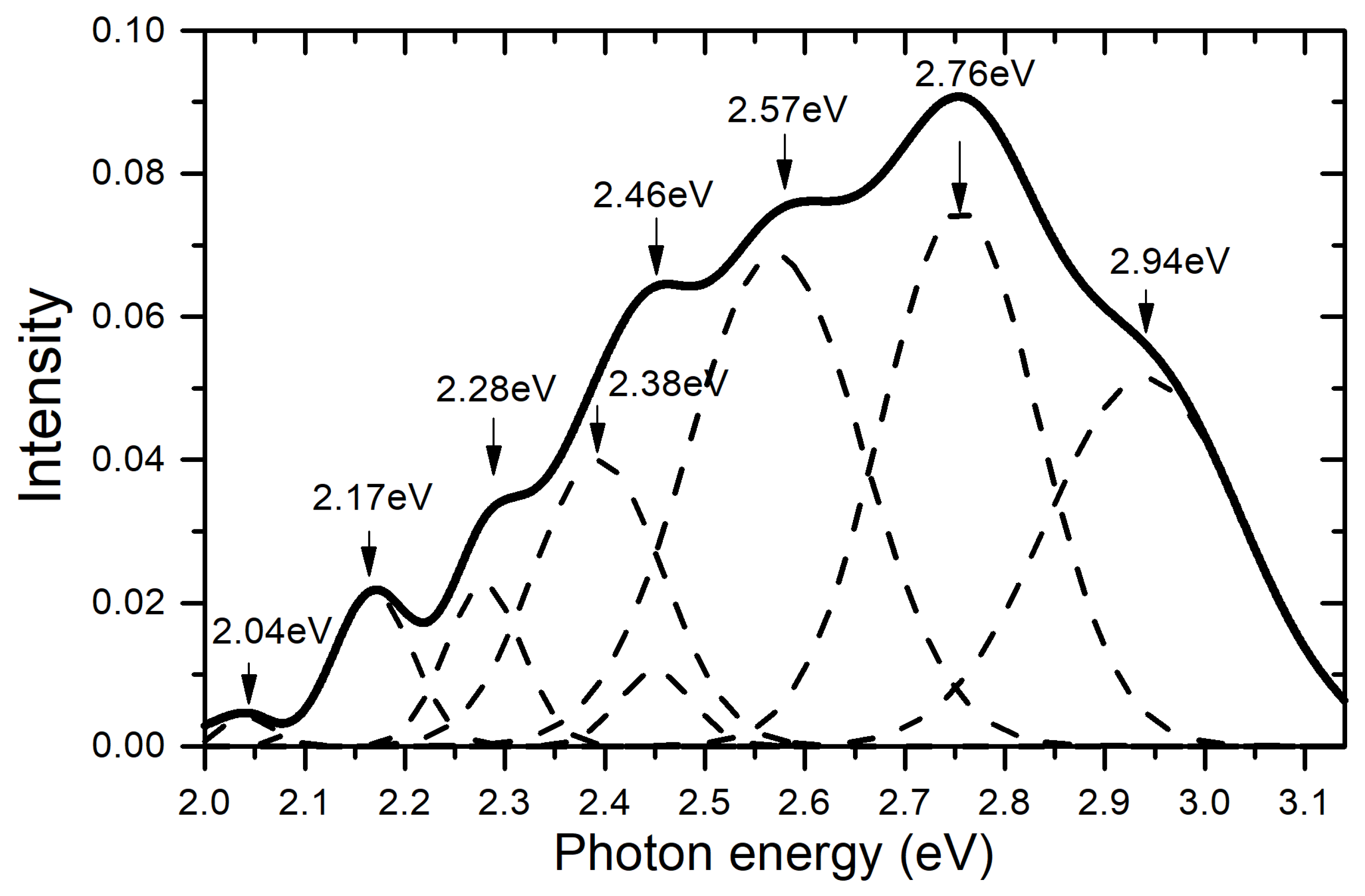
4. ZnSeO3/SiO2/Si Photoluminescence and Current–Voltage Characteristic
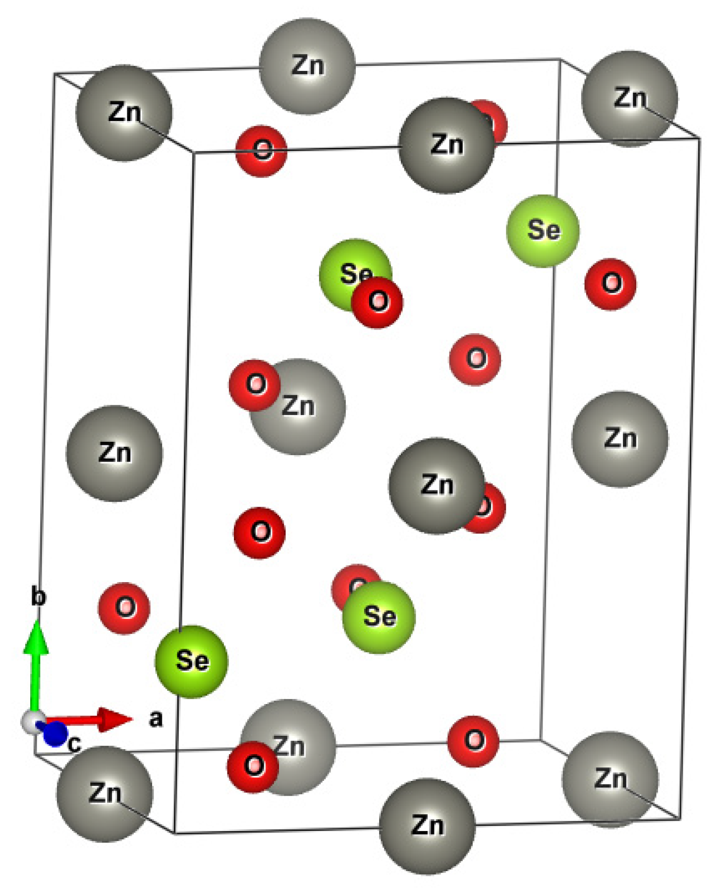
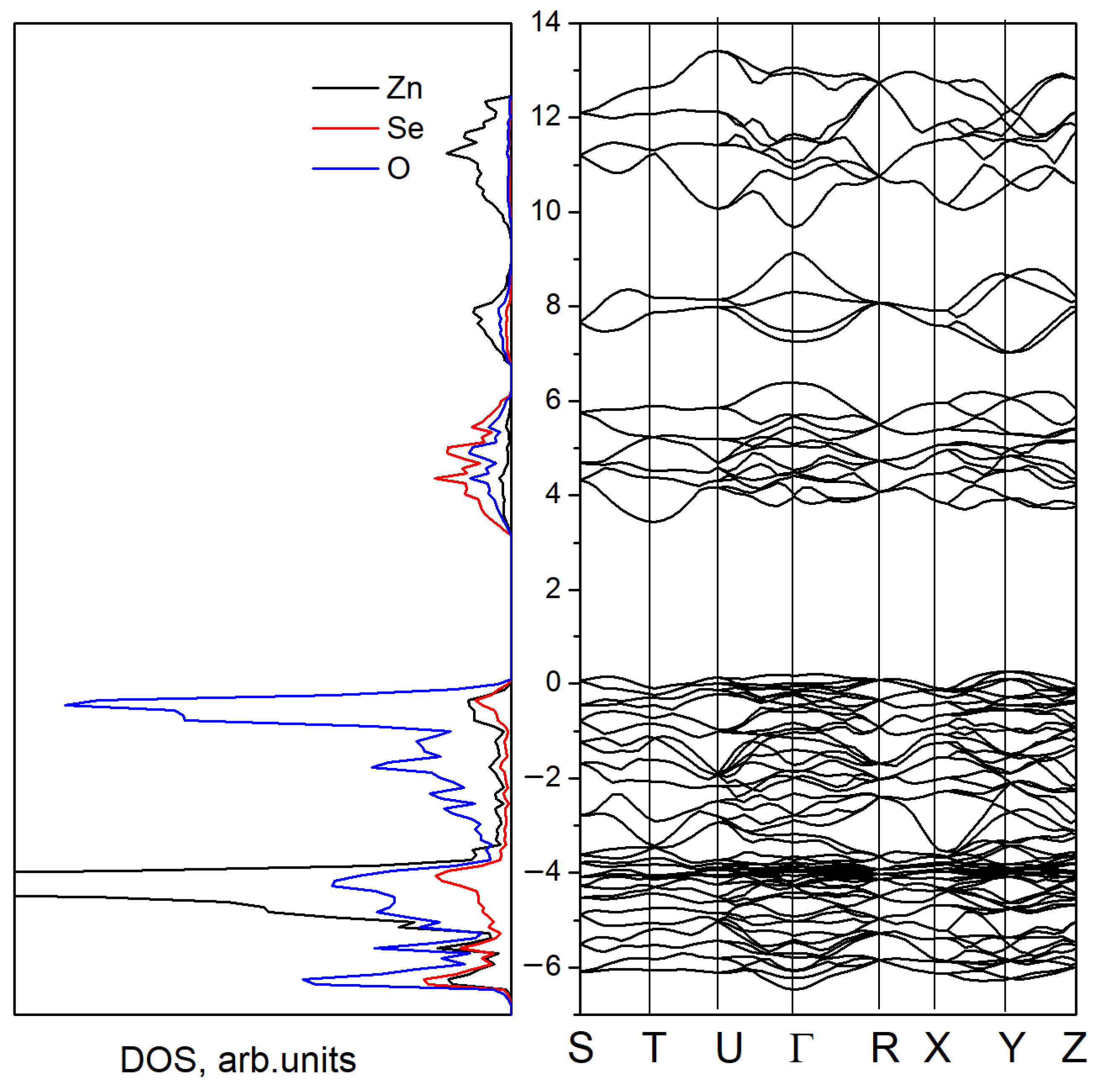
5. Computer Modeling of ZnSeO3
6. Conclusions
Author Contributions
Funding
Institutional Review Board Statement
Informed Consent Statement
Data Availability Statement
Acknowledgments
Conflicts of Interest
References
- Williams, J.S. Materials modification with ion beams. Rep. Prog. Phys. 1986, 49, 491–587. [Google Scholar] [CrossRef]
- Lang, M.; Tracy, C.L.; Palomares, R.I.; Zhang, F.; Severin, D.; Bender, M.; Trautmann, C.; Park, C.; Prakapenka, V.B.; Skuratov, V.A.; et al. Characterization of ion-induced radiation effects in nuclear materials using synchrotron X-ray techniques. J. Mater. Res. 2015, 30, 1366–1379. [Google Scholar] [CrossRef]
- Jain, I.P.; Agarwal, G. Ion beam induced surface and interface engineering. Surf. Sci. Rep. 2011, 66, 77–172. [Google Scholar] [CrossRef]
- Popov, A.; Lushchik, A.; Shablonin, E.; Vasil’Chenko, E.; Kotomin, E.; Moskina, A.; Kuzovkov, V. Comparison of the F-type center thermal annealing in heavy-ion and neutron irradiated Al2O3 single crystals. Nucl. Instrum. Methods Phys. Res. Sect. B Beam Interact. Mater. At. 2018, 433, 93–97. [Google Scholar] [CrossRef]
- Tanaka, A. Multiple Applications of Ion Beams in Life Science. Quantum Beam Sci. 2019, 3, 19. [Google Scholar] [CrossRef]
- Zhong, Y.; Dai, Y.; Shi, F.; Song, C.; Tian, Y.; Lin, Z.; Zhang, W.; Shen, Y. Effects of Ion Beam Etching on the Nanoscale Damage Precursor Evolution of Fused Silica. Materials 2020, 13, 1294. [Google Scholar] [CrossRef]
- van Vuuren, A.J.; Ibrayeva, A.D.; O’Connell, J.H.; Skuratov, V.A.; Mutali, A.; Zdorovets, M.V. Latent ion tracks in amorphous and radiation amorphized silicon nitride. Nucl. Instrum. Methods Phys. Res. Sect. B 2020, 473, 16–23. [Google Scholar] [CrossRef]
- Wen, Q.; Wei, X.; Jiang, F.; Lu, J.; Xu, X. Focused Ion Beam Milling of Single-Crystal Sapphire with A-, C-, and M-Orientations. Materials 2020, 13, 2871. [Google Scholar] [CrossRef]
- Kim, C.; Ahn, S.; Jang, D. Review: Developments in micro/nanoscale fabrication by focused ion beams. Vacuum 2012, 86, 1014–1035. [Google Scholar] [CrossRef]
- Córdoba, R. Editorial for the Special Issue on Nanofabrication with Focused Electron/Ion Beam Induced Processing. Micromachines 2021, 12, 893. [Google Scholar] [CrossRef]
- Kimura, K.; Sharma, S.; Popov, A. Fast electron–hole plasma luminescence from track-cores in heavy-ion irradiated wide-band-gap crystals. Nucl. Instrum. Methods Phys. Res. B 2002, 191, 48–53. [Google Scholar] [CrossRef]
- Schwartz, K.; Sorokin, M.V.; Lushchik, A.; Lushchik, C.; Vasil, E.; Papaleo, R.M.; Trautmann, C. Color center creation in LiF crystals irradiated with 5-and 10-MeV Au ions. Nucl. Instrum. Methods Phys. Res. B 2008, 266, 2736–2740. [Google Scholar] [CrossRef]
- Belianinov, A.; Burch, M.J.; Ievlev, A.; Kim, S.; Stanford, M.G.; Mahady, K.; Lewis, B.B.; Fowlkes, J.D.; Rack, P.D.; Ovchinnikova, O.S. Direct Write of 3D Nanoscale Mesh Objects with Platinum Precursor via Focused Helium Ion Beam Induced Deposition. Micromachines 2020, 11, 527. [Google Scholar] [CrossRef] [PubMed]
- Kotomin, E.A.; Kuzovkov, V.N.; Popov, A.I.; Vila, R. Kinetics of F center annealing and colloid formation in Al2O3. Nucl. Instrum. Methods Phys. Res. B 2016, 374, 107–110. [Google Scholar] [CrossRef]
- Hari, S.; Trompenaars, P.H.F.; Mulders, J.J.L.; Kruit, P.; Hagen, C.W. Combined Focused Electron Beam-Induced Deposition and Etching for the Patterning of Dense Lines without Interconnecting Material. Micromachines 2021, 12, 8. [Google Scholar] [CrossRef]
- Tomić Luketić, K.; Karlušić, M.; Gajović, A.; Fazinić, S.; O’Connell, J.H.; Pielić, B.; Radatović, B.; Kralj, M. Investigation of Ion Irradiation Effects in Silicon and Graphite Produced by 23 MeV I Beam. Materials 2021, 14, 1904. [Google Scholar] [CrossRef]
- Kotomin, E.; Kuzovkov, V.; Popov, A.I.; Maier, J.; Vila, R. Anomalous kinetics of diffusion-controlled defect annealing in irradiated ionic solids. J. Phys. Chem. A 2018, 122, 28–32. [Google Scholar] [CrossRef]
- Crespillo, M.L.; Graham, J.T.; Agulló-López, F.; Zhang, Y.; Weber, W.J. Real-Time Identification of Oxygen Vacancy Centers in LiNbO3 and SrTiO3 during Irradiation with High Energy Particles. Crystals 2021, 11, 315. [Google Scholar] [CrossRef]
- Lushchik, A.; Feldbach, E.; Kotomin, E.A.; Kudryavtseva, I.; Kuzovkov, V.N.; Popov, A.I.; Seeman, V.; Shablonin, E. Distinctive features of diffusion-controlled radiation defect recombination in stoichiometric magnesium aluminate spinel single crystals and transparent polycrystalline ceramics. Sci. Rep. 2020, 10, 7820. [Google Scholar]
- Laptev, R.; Svyatkin, L.; Krotkevich, D.; Stepanova, E.; Pushilina, N.; Lomygin, A.; Ognev, S.; Siemek, K.; Uglov, V. First-Principles Calculations and Experimental Study of H+-Irradiated Zr/Nb Nanoscale Multilayer System. Metals 2021, 11, 627. [Google Scholar] [CrossRef]
- Lorenz, M.; Rao, M.S.R.; Venkatesan, T.; Fortunato, E.; Barquinha, P.; Branquinho, R.; Salgueiro, D.; Martins, R.; Carlos, E.; Liu, A.; et al. The 2016 oxide electronic materials and oxide interfaces roadmap. J. Phys. D Appl. Phys. 2016, 49, 433001. [Google Scholar] [CrossRef]
- Coll, M.; Fontcuberta, J.; Althammer, M.; Bibes, M.; Boschker, H.; Calleja, A.; Cheng, G.; Cuoco, M.; Dittmann, R.; Dkhil, B.; et al. Towards oxide electronics: A roadmap. Appl. Surf. Sci. 2019, 482, 433001. [Google Scholar] [CrossRef]
- Toimil-Molares, M.E. Characterization and properties of micro-and nanowires of controlled size, composition, and geometry fabricated by electrodeposition and ion-track technology. Beilstein J. Nanotechnol. 2012, 3, 860–883. [Google Scholar] [CrossRef] [PubMed]
- Mo, D.; Liu, J.; Yao, H.; Duan, J.; Hou, M.; Sun, Y.; Chen, Y.; Xue, Z.; Zhang, L. Preparation and characterization of CdS nanotubes and nanowires by electrochemical synthesis in ion-track templates. J. Cryst. Growth 2008, 310, 612–616. [Google Scholar] [CrossRef]
- Ulrich, N.; Spende, A.; Burr, L.; Sobel, N.; Schubert, I.; Hess, C.; Trautmann, C.; Toimil-Molares, M.E. Conical Nanotubes Synthesized by Atomic Layer Deposition of Al2O3, TiO2, and SiO2 in Etched Ion-Track Nanochannels. Nanomaterials 2021, 11, 1874. [Google Scholar] [CrossRef] [PubMed]
- Spende, A.; Sobel, N.; Lukas, M.; Zierold, R.; Riedl, J.C.; Gura, L.; Schubert, I.; Moreno, J.M.M.; Nielsch, K.; Stühn, B.; et al. TiO2, SiO2, and Al2O3 coated nanopores and nanotubes produced by ALD in etched ion-track membranes for transport measurements. Nanotechnology 2015, 26, 335301. [Google Scholar] [CrossRef]
- Sobel, N.; Hess, C.; Lukas, M.; Spende, A.; Stühn, B.; Toimil-Molares, M.E.; Trautmann, C. Conformal SiO2 coating of sub-100 nm diameter channels of polycarbonate etched ion-track channels by atomic layer deposition. Beilstein J. Nanotechnol. 2015, 6, 472–479. [Google Scholar] [CrossRef]
- Panina, L.V.; Zagorskiy, D.L.; Shymskaya, A.; Doludenko, I.M.; Evstigneeva, S.A.; Melnikova, P.D.; Gilimyanova, A.R. 1D Nanomaterials in Fe-Group Metals Obtained by Synthesis in the Pores of Polymer Templates: Correlation of Structure, Magnetic, and Transport Properties. Phys. Status Solidi A 2022, 219, 2100538. [Google Scholar] [CrossRef]
- Dutt, S.; Apel, P.; Lizunov, N.; Notthoff, C.; Wen, Q.; Trautmann, C.; Mota-Santiago, P.; Kirby, N.; Kluth, P. Shape of nanopores in track-etched polycarbonate membranes. J. Membr. Sci. 2021, 638, 119681. [Google Scholar] [CrossRef]
- Zagorskiy, D.; Doludenko, I.; Zhigalina, O.; Khmelenin, D.; Kanevskiy, V. Formation of Nanowires of Various Types in the Process of Galvanic Deposition of Iron Group Metals into the Pores of a Track Membrane. Membranes 2022, 12, 195. [Google Scholar] [CrossRef]
- Blonskaya, I.; Lizunov, N.; Olejniczak, K.; Orelovich, O.; Yamauchi, Y.; Toimil-Molares, M.; Trautmann, C.; Apel, P. Elucidating the roles of diffusion and osmotic flow in controlling the geometry of nanochannels in asymmetric track-etched membranes. J. Membr. Sci. 2021, 618, 118657. [Google Scholar] [CrossRef]
- Golovanova, A.V.; Domnina, M.A.; Arzhanov, A.I.; Karimullin, K.R.; Eremchev, I.Y.; Naumov, A.V. AFM Characterization of Track-Etched Membranes: Pores Parameters Distribution and Disorder Factor. Appl. Sci. 2022, 12, 1334. [Google Scholar] [CrossRef]
- Yamaki, T.; Nuryanthi, N.; Kitamura, A.; Koshikawa, H.; Sawada, S.; Voss, K.-O.; Severin, D.; Trautman, C. Fluoropoly-mer-based nanostructured membranes created by swift-heavy-ion irradiation and their energy and environmental applications. Nucl. Instrum. Methods Phys. Res. Sect. B 2018, 435, 162–168. [Google Scholar] [CrossRef]
- Dauletbekova, A.; Vlasukova, L.; Baimukhanov, Z.; Akilbekov, A.; Kozlovskiy, A.; Giniyatova, S.H.; Seitbayev, A.; Usseinov, A.; Akylbekova, A. Synthesis of ZnO nanocrystals in SiO2/Si track template: Effect of electrodeposition parameters on structure. Physica Stat Solidi B 2019, 256, 1800408. [Google Scholar] [CrossRef]
- Giniyatova, S.; Dauletbekova, A.; Baimukhanov, Z.; Vlasukova, L.; Akilbekov, A.; Usseinov, A.; Kozlovskiy, A.; Akylbekova, A. Structure, electrical properties and luminescence of ZnO nanocrystals deposited in SiO2/Si track templates. Radiat. Meas. 2019, 125, 52–56. [Google Scholar] [CrossRef]
- Balakhayeva, R.; Akilbekov, A.; Baimukhanov, Z.; Usseinov, A.; Giniyatova, S.; Zdorovets, M.; Vlasukova, L.; Popov, A.I.; Dauletbekova, A. CdTe Nanocrystal Synthesis in SiO2/Si Ion-Track Template: The Study of Electronic and Structural Properties. Phys. Status Solidi A 2021, 218, 2000231. [Google Scholar] [CrossRef]
- Akilbekov, A.; Balakhayeva, R.; Zdorovets, M.; Baymukhanov, Z.; Komarov, F.F.; Karim, K.; Popov, A.I.; Dauletbekova, A. Ion track template technology for fabrication of CdTe and CdO nanocrystals. Nucl. Inst. Methods Phys. Res. B 2020, 481, 30–34. [Google Scholar] [CrossRef]
- Balakhayeva, R.; Akilbekov, A.; Baimukhanov, Z.; Giniyatova, S.; Zdorovets, M.; Gorin, Y.; Popov, A.I.; Dauletbekova, A. Structure properties of CdTe nanocrystals created in SiO2/Si ion track Templates. Surf. Coat. Technol. 2020, 401, 126269. [Google Scholar] [CrossRef]
- Ivanou, D.K.; Streltsov, E.A.; Fedotov, A.K.; Mazanik, A.V.; Fink, D.; Petrov, A. Electrochemical deposition of PbSe and CdTe nanoparticles onto p-Si(100) wafers and into nanopores in SiO2/Si(100) structure. Thin Solid Films 2005, 490, 154–160. [Google Scholar] [CrossRef]
- Akilbekov, A.; Akylbekova, A.; Usseinov, A.; Kozlovskyi, A.; Baymukhanov, Z.; Giniyatova, S.; Popov, A.I.; Dauletbekova, A. Ion track template technique for fabrication of ZnSe2O5 nanocrystals. Nuclear Instrum. Methods Phys. Res. B 2020, 476, 10–13. [Google Scholar] [CrossRef]
- Akylbekova, A.; Dauletbekova, A.; Baymukhanov, Z.; Kozlovsky, A.; Usseinov, A. Template synthesis of ZnSe2O5 nanocrystals. AIP Conf. Proc. 2019, 2174, 020001. [Google Scholar]
- Kaniukov, E.; Yakimchuk, D.; Arzumanyan, G.; Terryn, H.; Baert, K.; Kozlovskiy, A.; Zdorovets, M.; Belonogov, E.; Demyanov, S. Growth mechanisms of spatially separated copper dendrites in pores of a SiO2 template. Philos. Mag. 2017, 97, 2268–2283. [Google Scholar] [CrossRef]
- Demyanov, E.; Kaniukov, Y.E.; Petrov, A.V.; Belonogov, E.K.; Streltsov, E.A.; Ivanov, D.K.; Ivanova, Y.A.; Trautmann, C.; Terryn, H.; Petrova, M.; et al. On the morphology of Si/SiO2/Ni nanostructures with swift heavy ion tracks in silicon oxide. J. Surf. Investig. 2014, 8, 805–813. [Google Scholar] [CrossRef]
- Bundyukova, V.D. Porous SiO2/Si templates for the formation of plasmon nanostructures. In Proceedings of the Women scientists of Belarus and Kazakhstan: Materials of the International Scientific-Practical Conference, Minsk, Belarus, 1–2 March 2018; pp. 463–465. Available online: http://elib.bsu.by/handle/123456789/196112 (accessed on 25 February 2022).
- Bundyukova, V.D.; Yakimchuk, D.V.; Kaniukov, E.Y.; Tishkevich, D.I.; Kutuzau, M.D.; Prigodich, V.V.; Shemukhin, A.A.; Balakshin, Y.V.; Nazarov, A.V.; Kozhemiako, A.V.; et al. Modification of an SiO2(Au)/Si Surface by Irradiation with Argon Ions. Mosc. Univ. Phys. Bull. 2020, 75, 225–229. [Google Scholar] [CrossRef]
- Ashrafia, A.; Jagadish, C. Review of zincblende ZnO: Stability of metastable ZnO phases. J. Appl. Phys 2007, 102, 071101. [Google Scholar] [CrossRef]
- Uklein, A.; Multian, V.; Kuz’micheva, G.; Linnik, R.; Lisnyak, V.; Popov, A.; Gayvoronsky, V.Y. Nonlinear optical response of bulk ZnO crystals with different content of intrinsic defects. Opt. Mater. 2018, 84, 738–747. [Google Scholar] [CrossRef]
- Pashkevich, A.V.; Fedotov, A.K.; Poddenezhny, E.N.; Bliznyuk, L.A.; Fedotova, J.A.; Basov, N.A.; Kharchanka, A.A.; Zukowski, P.; Koltunowicz, T.N.; Korolik, O.V.; et al. Structure, electric and thermoelectric properties of binary ZnO-based ceramics doped with Fe and Co. J. Alloys Compd. 2022, 895, 162621. [Google Scholar] [CrossRef]
- Karbovnyk, I.; Sadoviy, B.; Turko, B.; Kostruba, A.M.; Luchechko, A.; Vasil’yev, V.S.; Kukhta, A.V. Optical properties of composite structure based on ZnO microneedles and Alq3 thin film. Opt. Quantum Electron. 2021, 53, 647. [Google Scholar] [CrossRef]
- Ostanina, T.N.; Rudoi, V.M.; Nikitin, V.S.; Darintseva, A.B.; Zalesova, O.L.; Porotnikova, N.M. Determination of the surface of dendritic electrolytic zinc powders and evaluation of its fractal dimension. Russ. J. Non-Ferr. Met. 2016, 57, 47–51. [Google Scholar] [CrossRef]
- Khaliullin, S.M.; Zhuravlev, V.D.; Ermakova, L.V.; Buldakova, L.Y.; Yanchenko, M.Y.; Porotnikova, N.M. Solution combustion synthesis of ZnO using binary fuel (glycine+ citric acid). Int. J. Self-Propagating High-Temp. Synth. 2019, 28, 226–232. [Google Scholar] [CrossRef]
- Borade, P.A.; Sant, T.; Gokarna, A.; Joshi, K.U.; Panat, R.P.; Jejurikar, S.M. Role of defects in modulating the near band edge emissions of sub-micron ZnO crystals. Opt. Mater. 2020, 109, 110348. [Google Scholar] [CrossRef]
- Rout, A.; Boltaev, G.S.; Ganeev, R.A.; Rao, K.S.; Fu, D.; Rakhimov, R.Y.; Kurbanov, S.S.; Urolov, S.Z.; Shaymardanov, Z.S.; Guo, C.; et al. Low-and high-order nonlinear optical studies of ZnO nanocrystals, nanoparticles, and nanorods. Eur. Phys. J. D 2019, 73, 235. [Google Scholar] [CrossRef]
- Sharopov, U.B.; Atabaev, B.G.; Djabbarganov, R. Defect Formation on the Surface of ZnO Using Low-Energy Electrons. J. Surf. Investig. X-Ray Synchrotron Neutron Tech. 2020, 14, 101–104. [Google Scholar] [CrossRef]
- El Filali, B.; Gomez, J.J.; Torchynska, T.V.; Espinola, J.C.; Shcherbyna, L. Band-edge emission, defects, morphology and structure of in-doped ZnO nanocrystal films. Opt. Mater. 2019, 89, 322–328. [Google Scholar] [CrossRef]
- Lin, Y.-P.; Polyakov, B.; Butanovs, E.; Popov, A.A.; Sokolov, M.; Bocharov, D.; Piskunov, S. Excited States Calculations of MoS2@ZnO and WS2@ZnO Two-Dimensional Nanocomposites for Water-Splitting Applications. Energies 2022, 15, 150. [Google Scholar] [CrossRef]
- Spataro, G.; Champouret, Y.; Florian, P.; Coppel, Y.; Kahn, M.L. Multinuclear solid-state NMR study: A powerful tool for understanding the structure of ZnO hybrid nanoparticles. Phys. Chem. Chem. Phys. 2018, 20, 12413–12421. [Google Scholar] [CrossRef]
- Jońca, J.; Ryzhikov, A.; Kahn, M.L.; Fajerwerg, K.; Chaudret, B.; Chapelle, A.; Fau, P. Shape-controlled ZnO nanostructures for gas sensing applications. Procedia Eng. 2014, 87, 907–910. [Google Scholar] [CrossRef][Green Version]
- Saliba, S.; Coppel, Y.; Davidson, P.; Mingotaud, C.; Chaudret, B.; Kahn, M.L.; Marty, J.D. Liquid crystal based on hybrid zinc oxide nanoparticles. J. Mater. Chem. 2011, 21, 6821–6823. [Google Scholar] [CrossRef]
- Carrey, J.; Carrere, H.; Kahn, M.L.; Chaudret, B.; Marie, X.; Respaud, M. Photoconductivity of self-assembled ZnO nanoparticles synthesized by organometallic chemistry. Semicond. Sci. Technol. 2007, 23, 025003. [Google Scholar] [CrossRef]
- Moorthy, S.; Moorthy, G.; Swaminathan, K. Fabrication of Novel ZnSeO3 Anchored on g-C3N4 Nanosheets: An Outstanding Photocatalyst for the Mitigation of Pesticides and Pharmaceuticals. J. Inorg. Organomet. Polym. Mater. 2020, 30, 4664–4676. [Google Scholar] [CrossRef]
- Hassan, S.A.; Bashir, S.; Zehra, K.; Ahmed, Q.S. Structural, morphological and optical properties of pulsed laser deposited ZnSe/ZnSeO3 thin films. Mater. Res. Express 2018, 5, 046404. [Google Scholar] [CrossRef]
- Jiang, H.Q.; Jun, C.H.E.; Li, Z.M.; Xi, Y.A.O. A reduction approach to prepare ZnSe nanocrystallites. Trans. Nonferrous Met. Soc. China 2006, 16, s419–s422. [Google Scholar] [CrossRef]
- Al’zhanova, A.; Dauletbekova, A.; Komarov, F.; Vlasukova, L.; Yuvchenko, V.; Akilbekov, A.; Zdorovets, M. Peculiarities of latent track etching in SiO2/Si structures irradiated with Ar, Kr and Xe ions. Nucl. Instrum. Methods Phys. Res. Sect. B Beam Interact. Mater. At. 2016, 374, 121–124. [Google Scholar] [CrossRef]
- Vlasukova, L.; Komarov, F.; Yuvchenko, V.; Baran, L.; Milchanin, O.; Dauletbekova, A.; Alzhanova, A.; Akilbekov, A. Etching of latent tracks in amorphous SiO2 and Si3N4: Simulation and experiment. Vacuum 2016, 129, 137–141. [Google Scholar] [CrossRef]
- Studenikin, S.A.; Golego, N.; Cocivera, M. Fabrication of green and orange photoluminescent, undoped ZnO films using spray pyrolysis. J. Appl. Phys. 1998, 84, 2287–2294. [Google Scholar] [CrossRef]
- Degoda, V.Y.; Sofienko, A.O. Specific features of the luminescence and conductivity of zinc selenide on exposure to X-ray and optical excitation. Semiconductors 2010, 44, 568–574. [Google Scholar] [CrossRef]
- Degoda, V.Y.; Podust, G.P.; Doroshenko, I.Y.; Pavlova, N.Y. Phosphorescence and conduction current relaxation in ZnSe crystals. Opt. Mater. 2022, 129, 112460. [Google Scholar] [CrossRef]
- Perdew, P.; Burke, K.; Ernzerhof, M. Generalized Gradient Approximation Made Simple. Phys. Rev. Lett. 1996, 77, 3865–3868. [Google Scholar] [CrossRef]
- Dovesi, R.; Saunders, V.R.; Roetti, R.; Orlando, R.; Zicovich-Wilson, C.M.; Pascale, F.; Civalleri, B.; Doll, K.; Harrison, N.M.; Bush, I.J.; et al. CRYSTAL14 User’s Manual University of Torino, Italy. Available online: http://www.crystal.unito.it. (accessed on 4 February 2022).
- Jaffe, J.E.; Hess, A.C. Hartree-Fock study of phase changes in ZnO at high pressure. Phys. Rev. B 1993, 48, 7903–7909. [Google Scholar] [CrossRef]
- Towler, M.D.; Zicovich-Wilson, C. Selenium Basis Set for the Crystal Program. Available online: https://vallico.net/mike_towler//basis_sets/Se_basis.txt (accessed on 4 March 2019).
- Gallino, G.; Pacchioni, C.; Valentin, D. Transition levels of defect centers in ZnO by hybrid functionals and localized basis set approach. J. Chem. Phys 2010, 133, 144512. [Google Scholar] [CrossRef]
- Van de Walle, C.G.; Neugebauer, J. First-principles calculations for defects and impurities: Applications to III-nitrides. J. Appl. Phys. 2004, 95, 3851–3879. [Google Scholar] [CrossRef]
- Mulliken, R.S. Electronic population analysis on LCAO-MO molecular wave functions. J. Chem. Phys. 1955, 23, 1833–1840. [Google Scholar] [CrossRef]
- Kohn, K.; Inoue, K.; Horie, O.; Akimoto, S. Crystal Chemistry of MSeO3 and MTeO3, (M = Mg, Mn, Co, Ni, Cu, and Zn). J. Solid State Chem. 1976, 18, 27–37. [Google Scholar] [CrossRef]


| No. | Type of Nanostructure | Method | References |
|---|---|---|---|
| 1 | ZnO nanocrystals with structures of sphalerite, wurtzite, and rock salt | Electrodeposition | [34,35] |
| 2 | CdTe nanocrystals | Electrodeposition, chemical deposition. Photoelectrochemical deposition | [36,37,38] |
| 3 | PbSe nanocrystals | Photoelectrochemical deposition | [39] |
| 3 | CdO nanocrystals | Chemical deposition | [37] |
| 4 | ZnSe2O5 nanocrystals | Electrodeposition | [40,41] |
| 5 | ZnSeO3 nanocrystals | Electrodeposition | present work |
| 6 | Cu and Ni nanocrystals | Electrodeposition | [42] |
| 7 | Layers of metallic Cu and Ni | Electrodeposition | [43] |
| 8 | Ag dendrites | Chemical deposition | [44] |
| 9 | Au nanostructures | Chemical deposition | [45] |
| No. | 2θ° | hkl | d, Å | The Size of Crystallites L, nm | Cell Parameters, Å | FWHM | Density ρ, (g/cm3) |
|---|---|---|---|---|---|---|---|
| 1 | 46.38 | 241 | 1.956 | 12.1 | 5.9231 7.6652 5.0400 | 1.11 | 5.584 |
| 2 | 46.67 56.27 61.54 | 241 341 350 | 1.945 1.6335 1.50561 | 70.3 | 5.9231 7.6652 5.0400 | 0.94 0.11 0.180 | 5.584 |
| 3 | 46.66 56.00 61.33 | 241 341 350 | 1.945 1.6406 1.5103 | 84.82 | 5.8640 7.5767 5.0026 | 0.95 0.14 0.16 | 5.588 |
| ED at 1.5 V | |||||
|---|---|---|---|---|---|
| (hkl) | 2θ° | d, Å | L, nm | Cell Parameters, Å | Degree of Crystallinity |
| 121 240 | 33.060 56.432 | 2.70738 1.62924 | 54.89 164.17 | a = 5.94052, b = 7.66370 c = 5.06273 | 68.5% |
| ED at 1.75 V | |||||
| 121 240 | 33.137 56.470 | 2.70130 1.62823 | 74.04 155.56 | a = 5.92538, b = 7.60209 c = 5.04784 | 70.8% |
| Parameter | This Work, Calc. | This Work, Exper. | Exper. [76] |
|---|---|---|---|
| a, Å | 5.85 | 5.90 | 5.92 |
| b, Å | 7.69 | 7.75 | 7.66 |
| c, Å | 5.19 | 5.04 | 5.04 |
| ρV (g/cm3) | 5.44 | 5.58 | - |
| qeff (Zn/Se/O) | +1.16/+1.36/−0.84 | - | - |
Publisher’s Note: MDPI stays neutral with regard to jurisdictional claims in published maps and institutional affiliations. |
© 2022 by the authors. Licensee MDPI, Basel, Switzerland. This article is an open access article distributed under the terms and conditions of the Creative Commons Attribution (CC BY) license (https://creativecommons.org/licenses/by/4.0/).
Share and Cite
Dauletbekova, A.; Akylbekova, A.; Sarsekhan, G.; Usseinov, A.; Baimukhanov, Z.; Kozlovskiy, A.; Vlasukova, L.A.; Komarov, F.F.; Popov, A.I.; Akilbekov, A.T. Ion-Track Template Synthesis and Characterization of ZnSeO3 Nanocrystals. Crystals 2022, 12, 817. https://doi.org/10.3390/cryst12060817
Dauletbekova A, Akylbekova A, Sarsekhan G, Usseinov A, Baimukhanov Z, Kozlovskiy A, Vlasukova LA, Komarov FF, Popov AI, Akilbekov AT. Ion-Track Template Synthesis and Characterization of ZnSeO3 Nanocrystals. Crystals. 2022; 12(6):817. https://doi.org/10.3390/cryst12060817
Chicago/Turabian StyleDauletbekova, Alma, Aiman Akylbekova, Gulnaz Sarsekhan, Abay Usseinov, Zein Baimukhanov, Artem Kozlovskiy, Liudmila A. Vlasukova, Fadey F. Komarov, Anatoli I. Popov, and Abdirash T. Akilbekov. 2022. "Ion-Track Template Synthesis and Characterization of ZnSeO3 Nanocrystals" Crystals 12, no. 6: 817. https://doi.org/10.3390/cryst12060817
APA StyleDauletbekova, A., Akylbekova, A., Sarsekhan, G., Usseinov, A., Baimukhanov, Z., Kozlovskiy, A., Vlasukova, L. A., Komarov, F. F., Popov, A. I., & Akilbekov, A. T. (2022). Ion-Track Template Synthesis and Characterization of ZnSeO3 Nanocrystals. Crystals, 12(6), 817. https://doi.org/10.3390/cryst12060817