Article

The Atomic Layer Etching Technique with Surface Treatment Function for InAlN/GaN Heterostructure

1
School of Microelectronics, Southern University of Science and Technology, Shenzhen 518055, China
2
Shenzhen Smartchip Microelectronics Technology Co., Ltd., Shenzhen 518045, China
3
Engineering Research Center of Integrated Circuits for Next-Generation Communications, Ministry of Education, Southern University of Science and Technology, Shenzhen 518055, China
4
GaN Device Engineering Technology Research Center of Guangdong, Southern University of Science and Technology, Shenzhen 518055, China
*
Author to whom correspondence should be addressed.
Crystals 2022, 12(5), 722; https://doi.org/10.3390/cryst12050722
Submission received: 17 April 2022 / Revised: 12 May 2022 / Accepted: 14 May 2022 / Published: 19 May 2022
(This article belongs to the Special Issue Semiconductor Nanocrystals)

Abstract

:
This paper studied an atomic layer etching (ALE) technique with a surface treatment function for InAlN/GaN heterostructures with AlN spacer layers. Various parameters were attempted, and 30 s O2 + 15 W BCl3 was chosen as the optimal recipe. The optimal ALE approach exhibited satisfactory etching results, with regard to the etch-stop effect, compared with other techniques. The atomic force microscopy (AFM) results showed an etching per cycle (EPC) value of 0.15 nm/cycle, with a 0.996 fit coefficient and root mean square (RMS) surface roughness of around 0.61 nm (0.71 nm for as-grown sample), which was the lowest in comparison with digital etching (0.69 nm), Cl2/BCl3 continuous etching (0.91 nm) and BCl3 continuous etching (0.89 nm). X-ray photoelectron spectroscopy (XPS) and scanning transmission electron microscopy with energy dispersive X-ray spectroscopy measurements (STEM/EDS) verified the indium clustered phenomena at the bottom apex of V-pit defects in the epi structure of InAlN/GaN high electron mobility transistors (HEMTs) for the first time, in addition to the surface morphology optimization for the ALE under-etching technique used in this work. The resistor hall effect (Hall) and AFM measurements demonstrated that after 4 or 5 ALE cycles, the two-dimensional electron gas (2-DEG) density and RMS roughness were improved by 15% and 11.4%, respectively, while the sheet resistance (Rsh) was reduced by 6.7%, suggesting a good surface treatment function. These findings were important for realizing high-performance InAlN/GaN HEMTs.

1. Introduction

InAlN/GaN-based high electron mobility transistors (HEMTs) have recently attracted much attention. Compared to the commonly used AlGaN/GaN heterostructure, the stronger spontaneous polarization effect of the InAlN/GaN heterostructure provides higher two-dimensional electron gas (2-DEG) density, leading to lower on-resistance (Ron) and a higher output current. Moreover, the lattice-matched In0.17Al0.83N/GaN heterostructure could also enhance device reliability. At the same time, enough 2-DEG density of InAlN/GaN contributes to a thinner barrier layer thickness, improving the radio frequency (RF) characteristics by reducing the short-channel effects of a deeply scaled device [1,2,3,4,5]. Owing to the advantages mentioned above, the InAlN/GaN heterostructure is considered as the most competitive candidate for GaN-based power and RF devices [6].
The etching technique is critical in GaN-based device fabrication, including the gate recess process, source/drain ohmic contact with a low annealing temperature, and regrown ohmic contact preparation. To relieve the serious etching damage and the resulting device reliability issues, an etching technique with a precisely controlled etching depth and low surface damage is urgently needed. In recent years, atomic layer etching (ALE) with two sequential quasi-self-limiting steps (O2 plasma modification step and BCl3 plasma removal step) has been used in the fabrication of AlGaN/GaN HEMTs, to obtain a well-controlled recess process and leakage current suppression, becoming a potential alternative to continuous dry etching and digital etching techniques [7,8,9,10,11,12,13,14,15,16]. However, little work has been reported on the study of ALE for the InAlN/GaN heterostructure. In our previous report, the O2/BCl3-based ALE technique for InAlN/GaN was proposed with good etching results [17]. However, systematic comparative studies among ALE, continuous dry etching, and digital etching techniques are still absent.
O2-based plasma treatment applied to InAlN/GaN HEMTs is an efficient surface treatment method for optimizing the output performance and leakage current of a device [2,18,19,20,21]. In 2011, Wang et al. reported, after 2 min of O2/Ar plasma treatment for the access region of the InAlN/GaN HEMTs, a high output current (2.1 A/mm) and low gate leakage (1 mA/mm), due to improvements in the electrical properties and trap state passivation. The electrical property optimizations of 2-DEG density and sheet resistance (Rsh) were similar to the AlGaN/GaN heterostructure passivated by SiN [18]. Moreover, in 2011, Lee et al. reduced the gate leakage of InAlN/GaN HEMTs by more than two orders of magnitude by using O2 plasma inductively coupled plasma (ICP) Asher treatment on the InAlN surface after ohmic preparation, which was similar to the results in the AlGaN device [19]. In 2016, using 5 min of O2 reactive ion etching (RIE) plasma treatment before gate metallization, Ma et al. fabricated InAlN/GaN HEMT with an output current of 2.18 A/mm and gate leakage of 10−2 mA/mm, which resulted in defect suppression and barrier height increase [2]. In 2021, with 1 min of O2 RIE plasma treatment prior to gate deposition by Asher, Cui et al. realized an InAlN/GaN HEMT with a high Ion/Ioff ratio of ~107 and low surface leakage [21]. A thin In2O3 and Al2O3 mixed oxide layer on the InAlN surface could increase the effective barrier height of InAlN and decrease the trap density of the surface, optimizing the electrical properties (2-DEG density and Rsh) of the epitaxy, while also leading to enhancement of the device performances, such as the output current and Ron, and suppressing the gate leakage [18,22,23,24]. Therefore, the ALE technique with an O2 modification step has potential for surface treatment functions.
In this paper, an O2/BCl3-based ALE technique for the InAlN/GaN heterostructure with a surface treatment function was studied. An etching per cycle (EPC) value of 0.15 nm/cycle, with a fit (R2) coefficient of 0.996, was obtained. The InAlN surface root mean square (RMS) roughness after the ALE (0.61 nm) process was lower than the samples obtained using digital etching (0.69 nm), Cl2/BCl3 (0.91 nm) etching, and BCl3 (0.89 nm) etching techniques. Four or five cycles of ALE surface treatment on an as-grown InAlN wafer resulted in the 2-DEG density improving by 15%, Rsh reducing by 6.7%, and surface RMS roughness optimizing by 11.4%. The mechanism was systematically investigated by the following measurements: atomic force microscopy (AFM), resistor Hall effect (Hall) measurement, X-ray photoelectron spectroscopy (XPS), and scanning transmission electron microscopy (STEM) with energy dispersive X-ray spectroscopy (EDS).

2. Experimental

Sample preparation: The 6″ In0.17Al0.83N/GaN wafer was grown on high-resistivity Si substrate for device fabrication, which was purchased from NTT AT Corporation. As shown in Figure 1a, a 10.6 nm In0.17Al0.83N barrier layer and a 1 nm AlN spacer layer were grown on a 1000 nm i-GaN channel layer to form the 2-DEG characterization. Figure 1b and c show the STEM image of the InAlN wafer. The 6″ wafer was diced into 2 × 2 cm2 and 1 × 1 cm2 samples. The former were used for etching experiments with AFM measurement, and the latter were used for XPS, STEM/EDS measurements and surface treatment experiments with AFM and Hall measurements.
As shown in Figure 2(a1), a 300 nm SiO2 hard mask for the ALE process was deposited on 2 × 2 cm2 samples by plasma-enhanced chemical vapor deposition (PECVD) at 350 °C. Photolithography was utilized for determining the desired pattern. In order to remove the SiO2 mask selectively, SF6 plasma ICP-RIE was performed.
Parameter settings: The O2 plasma modification step and BCl3 plasma removal step of the O2/BCl3 ALE approach are shown in Figure 2(a2,a3), respectively. For the modification step, the parameters were set at the following: ICP power = 100 W and RF power = 50 W, while the modification time was variable. For the removal step, the parameters were set at the following: ICP power = 0 W and RF power = 15 W, with the removal time at 30 s. These two steps were performed in sequence, alternatively, in the Corial 210IL 200 mm ICP system at a chamber pressure of 10 mTorr and gas flow rate of 50 sccm, with 30 s switching time. After the whole etching process, the SiO2 hard mask was removed by buffered oxide etch (BOE), as shown in Figure 2(a4).
The EPC and surface roughness were measured for samples with various O2 modification times to determine the optimal parameters for the ALE technique. In Figure 3a, as the modification time increased, EPC firstly increased and then tended to saturate, while the RMS roughness firstly reduced and then stabilized gradually. Given the production efficiency, an O2 modification time of 30 s was determined for the ALE recipe. Figure 3b demonstrates the initial calibration of this ALE technique with optimal parameters (30 s O2 modification time), and good repeatability of single atomic-level EPC (0.15 nm/cycle) was confirmed by R2 = 0.996 and low dispersion.
Three representative etching techniques were used as the control groups for the ALE technique. For the digital etching technique, the process combined O2 plasma oxidation followed by the oxidation layer being removed using diluted HCl solution, as shown in Figure 2(b1–b4). For the Cl2/BCl3 and BCl3 continuous etching techniques shown in Figure 2(c1–c3), the RF/ICP power was set at 15/100 W and 15/0 W, respectively. Thus, five samples were prepared accordingly: as-grown (sample 0, S0), ALE (sample 1, S1), digital etching (sample 2, S2), Cl2/BCl3 continuous etching (sample 3, S3), and BCl3 continuous etching (sample 4, S4).
Characterization: The surface roughness was measured immediately after etching, and then after removing the SiO2 mask, the etching depth was measured by AFM. XPS measurements were performed to investigate the ALE mechanism. Moreover, the as-grown epi wafer was measured by STEM/EDS to verify the epitaxy characteristics of the InAlN/GaN heterostructure. To explore the effect of ALE surface treatment, Ti/Al/Ti/Au (20/110/40/50 nm) metal electrodes were deposited at four corners of the samples after variable cycles of ALE surface treatment, and 45 s of 860 °C N2 rapid thermal annealing (RTA) was used to reduce the contact resistance for Hall measurements.

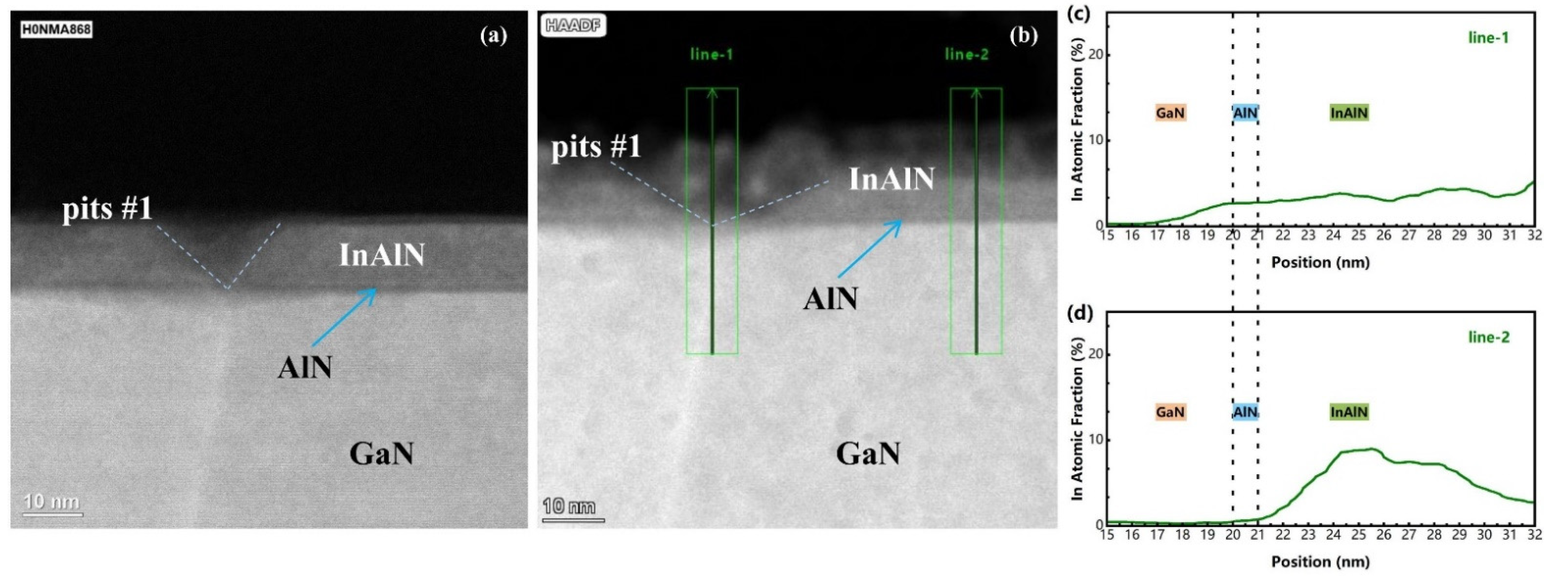
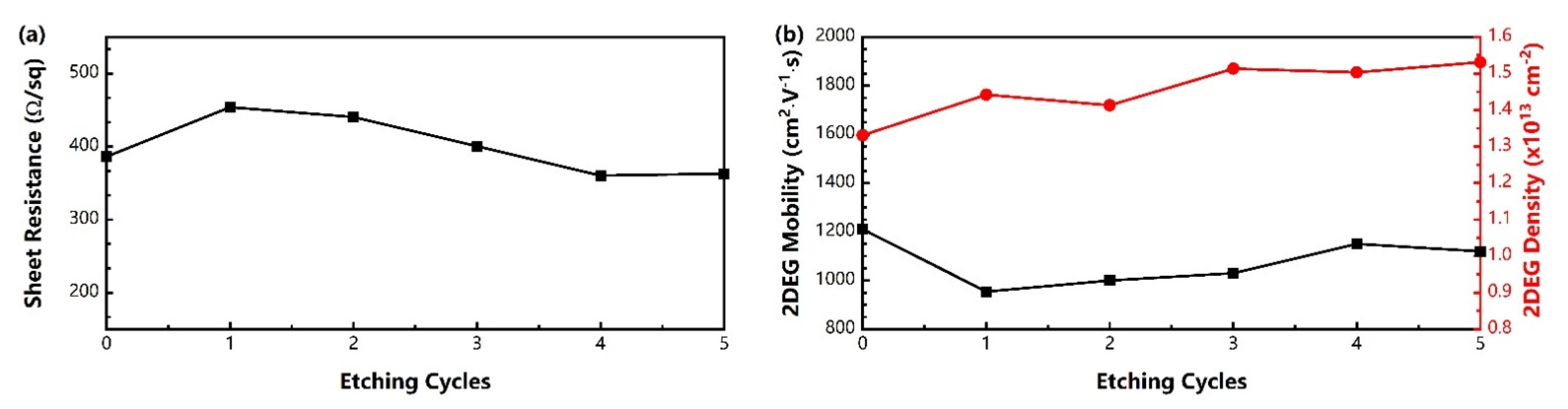
3. Results and Discussion

The etching depth vs. etching cycles for samples S1–2 and the etching depth vs. etching time for samples S3–4 are shown in Figure 4, while the corresponding EPCs (nm/cycle) or etching rates (nm/min) for the InAlN, AlN and GaN layers are listed in Table 1. The EPCs of the InAlN, AlN and GaN layers for sample S1 were 0.15, 0.03 and 0.46 nm/cycle, respectively. An obvious etch-stop phenomenon was observed during the ALE process, as shown in Figure 4a, which could be explained by the efficient blocking function of the AlN layer with poor oxidation properties [17,25]. For sample S2 in Figure 4b, the EPC of the InAlN layer was up to 7.46 nm/cycle, and the InAlN layer could be over etched by only two cycles of digital etching. Although the EPC of sample S2 decreased around the AlN layer, no etch-stop effect was observed, as opposed to AlGaN/GaN. This suggests that only the ALE technique can provide an etch-stop effect on the InAlN/GaN heterostructure, further explained below by the STEM image of the InAlN/GaN heterojunction. As shown in Figure 4c,d, due to the existence of Cl2 plasma, the etching rate of sample S3 (17.88 nm/min) was much bigger than that of sample S4 (0.28 nm/min). Nevertheless, both these continuous etching techniques consisted of linear etching processes during the whole InAlN/GaN etching process. With the stable InAlN EPC shown in Figure 3b and etch-stop effect at the AlN layer, the ALE technique of sample S1 was confirmed as the most effective way for controlling the InAlN/GaN etching depth precisely, compared to the other three etching techniques.
Figure 5a−f show the surface morphology for the as-grown InAlN surface of sample S0, InAlN etched surface of sample S1–4, and AlN etched surface of sample S1. All the InAlN etched surface morphologies were obtained at an etching depth of approximately 9 nm, while the AlN etched surface morphology of sample S1 was measured at an etching depth of around 11.5 nm, which is in the AlN layer. The corresponding RMS and mean roughness are listed in Table 2. For sample S1, the InAlN and AlN etched surfaces after the ALE process showed similar RMS roughness values (0.61 nm and 0.60 nm), which were even lower than that of sample S0 (0.71 nm). Compared to sample S2 (0.69 nm), obtained using the digital etching technique, sample S1 had lower roughness and dispersion (as shown in Figure 5g,h), further demonstrating that the ALE technique with quasi-self-limiting characteristics is more stable in controlling the surface morphology. Compared to samples S3 (0.91 nm) and S4 (0.89 nm), the ALE technique provided a much smoother surface by effectively overcoming the continuous etching limitations, such as transport-limited phenomena, highly coupled parameters, and propagation of the damaged etch front, which could be beneficial to decrease the interface trap density and device leakage current [7,12]. The ALE technique was the most effective way to control the InAlN/GaN etching surface morphology.
To systematically explore the mechanism of the ALE technique, XPS measurements of Al and In oxides were performed on an InAlN/GaN wafer for one cycle of ALE, as shown in Figure 6. For the Al element in Figure 6a, after one O2 modification step of sample S1, the Al2O3 content increased significantly compared to sample S0, whereas a substantially reduced Al2O3 content was observed after the following BCl3 etching of sample S1. The In2O3 content shown in Figure 6b had the same change as Al2O3. These results indicate the oxidation function of the ALE modification step and the effective etching of the ALE removal step. Moreover, the Al2O3 and In2O3 contents after one ALE cycle of sample S1 were more than the as-grown sample S0. This implies that the ALE technique used in this work was an under-etching approach, which did not completely remove the oxides formed by the O2 modification step.
For the first time, Figure 7a shows the STEM image of an epi structure of InAlN/GaN HEMTs with V-pit defects penetrating through the whole InAlN barrier layer. V-pits are usually generated on the dislocations of bottom GaN, leading to poor surface morphology (as shown in Figure 5) of the InAlN epilayer, and were hardly observed in the AlGaN/GaN heterojunction [26,27]. Figure 7c,d show the EDS results of the indium (In) atomic fraction for the InAlN/GaN heterostructure at the V-pit position (line-1) and general position (line-2) (Figure 7b). The In element was observed in the AlN/GaN region below the V-pits and was absent in the general position, verifying the In clustered phenomenon was the origin of V-pit defects [28,29]. The In elements involvement made the AlN more easily oxidized, due to the lower binding energy of In-O, and the large number of V-pits provided excessive oxidation paths of AlN in the digital etching technique, leading to loss of the etch-stop effect. The ALE technique with only 30 s of oxidation could effectively avoid this problem, which was well matched with the results shown in Figure 4a,b. Furthermore, the observed In clustered phenomenon at the V-pit apex could demonstrate why the under-etching ALE technique (oxide residue after etching) achieved better surface morphology than the over-etching ALE technique (no oxide residue after etching) in our previous work [17].
The surface treatment function of the ALE process for an InAlN/GaN heterostructure was also investigated. In Figure 8 and Table 3, the electrical properties, including the Rsh, 2-DEG mobility and density, of the as-grown sample S0 and sample S1 with 1–5 cycles of ALE surface treatment are demonstrated. The Rsh increased to 454 Ω/sq for one cycle of treatment, which was above the as-grown Rsh (386 Ω/sq), and then decreased steadily from 454 Ω/sq to around 360 Ω/sq from one cycle to five cycles of treatment, while the 2-DEG mobility exhibited an almost opposite trend to Rsh, and finally recovered close to the as-grown 2-DEG mobility (1210 cm2·V−1·s) for treatment of 1–5 cycles. These trends are closely related to the interface scattering changes represented by the surface morphology roughness shown in Table 3. The increasement in RMS roughness enhanced the interface scattering, thus causing Rsh and 2-DEG mobility to worsen, and vice versa. However, the 2-DEG density continuously increased from 1.33 × 1013 cm−2 to 1.53 × 1013 cm−2 for 1–5 cycles of ALE surface treatment with only 0.75 nm InAlN etch amount. Since the ALE technique in this work was an under-etching approach, it would gradually generate a thin oxide layer with a high O content for 1–5 cycles of treatment, similarly to O2-based plasma surface treatment, which could reduce the surface barrier height of the nitrides and increase the effective barrier height, thereby subsequently increasing the 2-DEG density [18,22]. Thus, compared to sample S0, sample S1 with four or five cycles of ALE surface treatment could reduce Rsh by 6.7% and increase the 2-DEG density by 15%, which was comparable to the optimization ability of the reported O2 plasma surface treatment and other treatment approaches [18,30,31]. In addition, lower RMS roughness of 0.39 nm was obtained after four or five cycles of treatment, compared to sample S0 (0.44 nm). This demonstrates that the ALE technique had an efficient surface treatment function to make InAlN/GaN HEMTs reduce Ron, gate leakage and increase output current density.

4. Conclusions

In summary, this paper demonstrates an ALE technique with a surface treatment function for InAlN/GaN heterostructures. This ALE technique obtained well-controlled EPC (0.15 nm/cycle) and improved the surface RMS roughness (0.61 nm), which was much lower than that of the as-grown sample (0.71 nm), digital etching (0.69 nm), Cl2/BCl3 etching (0.91 nm) and BCl3 etching techniques (0.89 nm). The XPS and STEM/EDS results confirmed the In clustered phenomenon below the V-pit defects, which was related to the surface morphology optimization of the under-etching ALE technology used in this work. Hall and AFM measurements verified the effective ALE surface treatment function on the InAlN/GaN heterostructure. A maximum reduction of 6.7% in Rsh and a maximum increasement of 15% in 2-DEG density, with surface roughness optimization of 11.4%, were obtained after four or five cycles of treatment. This enabled high-performance InAlN/GaN HEMTs designs to be obtained.

Author Contributions

Conceptualization, F.D. and Q.W.; data curation, H.L., Q.H., X.T. and H.H.; formal analysis, F.D.; funding acquisition, H.Y. and Q.W.; investigation, F.D., Z.W. and C.T.; methodology, Y.J.; project administration, Q.W.; resources, Z.W.; supervision, H.Y. and Q.W.; validation, Y.J., H.L., J.H. and K.W.; writing—original draft, F.D.; writing—review and editing, Q.W. All authors have read and agreed to the published version of the manuscript.

Funding

This research was funded by Research on R&D and industrialization of new energy vehicle drive and its special chip for charging pile (Grant No. 2019B010143001), Research and Application of Key Technologies of GaN-based Power Devices on Si Substrate (Key-Area Research and Development Program of GuangDong Province, Grant No: 2019B010128001), Research on key technologies for optimization of IoT chips and product development (Key-Area Research and Development Program of GuangDong Province, Grant No:2019B010142001), Research on the fabrication and mechanism of GaN power and RF devices (Grant No: JCYJ20200109141233476), Research on the GaN Chip for 5G Application (Grant No: JCYJ20210324120409025), Research on high-reliable GaN power device and the related industrial power system (Grant No: HZQB-KCZYZ-2021052) and Special Funds for the Cultivation of Guangdong College Students’ Scientific and Technological Innovation. (“Climbing Program” Special Funds) pdjh2022c0073.

Institutional Review Board Statement

Not applicable.

Informed Consent Statement

Not applicable.

Data Availability Statement

The data presented in this study are available on request from the corresponding author.

Acknowledgments

This work was supported by Research on R&D and industrialization of new energy vehicle drive and its special chip for charging pile (Grant No. 2019B010143001), Research and Application of Key Technologies of GaN-based Power Devices on Si Substrate (Key-Area Research and Development Program of GuangDong Province, Grant No: 2019B010128001), Research on key technologies for optimization of IoT chips and product development (Key-Area Research and Development Program of GuangDong Province, Grant No:2019B010142001), Research on the fabrication and mechanism of GaN power and RF devices (Grant No: JCYJ20200109141233476), Research on the GaN Chip for 5G Application (Grant No: JCYJ20210324120409025), Research on high-reliable GaN power device and the related industrial power system (Grant No: HZQB-KCZYZ-2021052) and Special Funds for the Cultivation of Guangdong College Students’ Scientific and Technological Innovation. (“Climbing Program” Special Funds) pdjh2022c0073. The authors acknowledge the assistance of SUSTech Core Research Facilities.

Conflicts of Interest

The authors declare no conflict of interest. The funders had no role in the design of the study; in the collection, analyses, or interpretation of data; in the writing of the manuscript, or in the decision to publish the results.

References

  1. Huang, Y.-P.; Hsu, W.-C.; Liu, H.-Y.; Lee, C.-S. Enhancement-Mode Tri-Gate Nanowire InAlN/GaN MOSHEMT for Power Applications. IEEE Electron Device Lett. 2019, 40, 929–932. [Google Scholar] [CrossRef]
  2. Ma, C.; Gu, G.; Lü, Y. A high performance InAlN/GaN HEMT with low Ron and gate leakage. J. Semicond. 2016, 37, 024099. [Google Scholar] [CrossRef]
  3. Chiu, H.-C.; Wu, C.-H.; Chi, J.-F.; Chyi, J.I.; Lee, G.Y. N2O treatment enhancement-mode InAlN/GaN HEMTs with HfZrO2 High-k insulator. Microelectron. Reliab. 2015, 55, 48–51. [Google Scholar] [CrossRef]
  4. Wang, R.; Saunier, P.; Xing, X.; Lian, C.; Gao, X.; Guo, S.; Snider, G.; Fay, P.; Jena, D.; Xing, H. Gate-Recessed Enhancement-Mode InAlN/AlN/GaN HEMTs With 1.9-A/mm Drain Current Density and 800-mS/mm Transconductance. IEEE Electron Device Lett. 2010, 31, 1383–1385. [Google Scholar] [CrossRef]
  5. Chung, J.W.; Saadat, O.I.; Tirado, J.M.; Xiang, G.; Guo, S.; Palacios, T. Gate-Recessed InAlN/GaN HEMTs on SiC Substrate With Al2O3 Passivation. IEEE Electron Device Lett. 2009, 30, 904–906. [Google Scholar] [CrossRef]
  6. Gu, G.; Cai, Y.; Feng, Z.; Liu, B.; Zeng, C.; Yu, G.; Dong, Z.; Zhang, B. Enhancement-mode InAlN/GaN MISHEMT with low gate leakage current. J. Semicond. 2012, 33, 064044. [Google Scholar] [CrossRef]
  7. Hu, Q.; Li, S.; Li, T.; Wang, X.; Li, X.; Wu, Y. Channel Engineering of Normally-OFF AlGaN/GaN MOS-HEMTs by Atomic Layer Etching and High-k Dielectric. IEEE Electron Device Lett. 2018, 39, 1377–1380. [Google Scholar] [CrossRef]
  8. Hwang, I.-H.; Cha, H.-Y.; Seo, K.-S. Low-Damage and Self-Limiting (Al)GaN Etching Process through Atomic Layer Etching Using O2 and BCl3 Plasma. Coatings 2021, 11, 268. [Google Scholar] [CrossRef]
  9. Tang, J.; Hu, Y.; Zhang, Y.; Gu, Z.; Che, D.; Hu, D.; Chen, L.; Xu, K.; Zhuang, S. XPS Analysis of Gallium Nitride Film After O2/BCl3 Digital Etch. In Proceedings of the China Semiconductor Technology International Conference (CSTIC), Shanghai, China, 26 June–17 July 2020. [Google Scholar]
  10. Mikhailovich, S.V.; Pavlov, A.Y.; Tomosh, K.N.; Fedorov, Y.V. Low-Energy Defectless Dry Etching of the AlGaN/AlN/GaN HEMT Barrier Layer. Tech. Phys. Lett. 2018, 44, 435–437. [Google Scholar] [CrossRef]
  11. Kai, Z.; Zhou, J.; Cen, K.; Kong, Y.; Chen, T. Enhancement-mode Al2O3/InAlGaN/GaN MOS-HEMTs with a record drain current density of 1.7 A/mm and a threshold voltage of +1.5 V. In Proceedings of the China International Forum on Solid State Lighting: International Forum on Wide Bandgap Semiconductors China (SSLChina: IFWS), Beijing, China, 15–17 November 2016. [Google Scholar]
  12. Kanarik, K.J.; Lill, T.; Hudson, E.A.; Sriraman, S.; Tan, S.; Marks, J.; Vahedi, V.; Gottscho, R.A. Overview of atomic layer etching in the semiconductor industry. J. Vac. Sci. Technol. A Vac. Surf. Film. 2015, 33, 020802. [Google Scholar] [CrossRef] [Green Version]
  13. Burnham, S.D.; Boutros, K.; Hashimoto, P.; Butler, C.; Wong, D.W.S.; Hu, M.; Micovic, M. Gate-recessed normally-off GaN-on-Si HEMT using a new O2-BCl3 digital etching technique. Phys. Status Solidi (C) 2010, 7, 2010–2012. [Google Scholar] [CrossRef]
  14. Wu, J.; Lei, S.; Cheng, W.C.; Sokolovskij, R.; Wang, Q.; Xia, G.; Yu, H. Oxygen-based digital etching of AlGaN/GaN structures with AlN as etch-stop layers. J. Vac. Sci. Technol. A Vac. Surf. Films 2019, 37, 060401. [Google Scholar] [CrossRef] [Green Version]
  15. Huang, Y.-P.; Lee, C.-S.; Hsu, W.-C. Enhancement-Mode InAlN/GaN Power MOSHEMT on Silicon With Schottky Tri-Drain Extension. IEEE Electron Device Lett. 2020, 41, 1048–1051. [Google Scholar] [CrossRef]
  16. Freedsman, J.J.; Watanabe, A.; Ito, T.; Egawa, T. Recessed gate normally-OFF Al2O3/InAlN/GaN MOS-HEMT on silicon. Appl. Phys. Express 2014, 7, 104101. [Google Scholar] [CrossRef]
  17. Du, F.; Jiang, Y.; Qiao, Z.; Wu, Z.; Tang, C.; He, J.; Zhou, G.; Cheng, W.-C.; Tang, X.; Wang, Q.; et al. Atomic layer etching technique for InAlN/GaN heterostructure with AlN etch-stop layer. Mater. Sci. Semicond. Process. 2022, 143, 106544. [Google Scholar] [CrossRef]
  18. Wang, R.; Li, G.; Laboutin, O.; Cao, Y.; Johnson, W.; Snider, G.; Fay, P.; Jena, D.; Xing, H. 210-GHz InAlN/GaN HEMTs With Dielectric-Free Passivation. IEEE Electron Device Lett. 2011, 32, 892–894. [Google Scholar] [CrossRef]
  19. Lee, D.S.; Chung, J.W.; Wang, H.; Gao, X.; Guo, S.; Fay, P.; Palacios, T. 245-GHz InAlN/GaN HEMTs With Oxygen Plasma Treatment. IEEE Electron Device Lett. 2011, 32, 755–757. [Google Scholar] [CrossRef]
  20. Lee, D.S.; Gao, X.; Guo, S.; Palacios, T. InAlN/GaN HEMTs With AlGaN Back Barriers. IEEE Electron Device Lett. 2011, 32, 617–619. [Google Scholar] [CrossRef]
  21. Cui, P.; Zeng, Y. Technology of sub-100 nm InAlN/GaN HEMTs on silicon with suppressed leakage current. Solid-State Electron. 2021, 185, 108137. [Google Scholar] [CrossRef]
  22. Yang, L.; Zhang, B.; Li, Y.; Chen, D. Improved Schottky barrier characteristics for AlInN/GaN diodes by oxygen plasma treatment. Mater. Sci. Semicond. Process. 2018, 74, 42–45. [Google Scholar] [CrossRef]
  23. Turuvekere, S.; Karumuri, N.; Rahman, A.A.; Bhattacharya, A.; DasGupta, A.; DasGupta, N. Gate Leakage Mechanisms in AlGaN/GaN and AlInN/GaN HEMTs: Comparison and Modeling. IEEE Trans. Electron Devices 2013, 60, 3157–3165. [Google Scholar] [CrossRef]
  24. Zhao, S.L.; Hou, B.; Chen, W.W.; Mi, M.H.; Zheng, J.X.; Zhang, J.C.; Ma, X.H.; Hao, Y. Analysis of the Breakdown Characterization Method in GaN-Based HEMTs. IEEE Trans. Power Electron. 2016, 31, 1517–1527. [Google Scholar] [CrossRef]
  25. Buttari, D.; Chini, A.; Palacios, T.; Coffie, R.; Shen, L.; Xing, H.; Heikman, S.; Mccarthy, L.; Chakraborty, A.; Keller, S. Origin of etch delay time in Cl2 dry etching of AlGaN/GaN structures. Appl. Phys. Lett. 2003, 83, 4779–4781. [Google Scholar] [CrossRef]
  26. Chen, Z.; Fujita, K.; Ichikawa, J.; Egawa, T. Threading dislocation-governed degradation in crystal quality of heteroepitaxial materials: The case of InAlN nearly lattice-matched to GaN. J. Appl. Phys. 2012, 111, 053535. [Google Scholar] [CrossRef]
  27. Hiroki, M.; Maeda, N.; Kobayashi, T. Electrical properties and device characteristics of InAlN/AlGaN/ AlN/GaN heterostructure field effect transistors. Phys. Status Solidi 2010, 6, S1056–S1060. [Google Scholar] [CrossRef]
  28. Minj, A.; Cavalcoli, D.; Cavallini, A. Indium segregation in AlInN/AlN/GaN heterostructures. Appl. Phys. Lett. 2010, 97, 132114. [Google Scholar] [CrossRef]
  29. Kehagias, T.; Dimitrakopulos, G.P.; Kioseoglou, J.; Kirmse, H.; Giesen, C.; Heuken, M.; Georgakilas, A.; Neumann, W.; Karakostas, T.; Komninou, P. Indium migration paths in V-defects of InAlN grown by metal-organic vapor phase epitaxy. Appl. Phys. Lett. 2009, 95, 071905. [Google Scholar] [CrossRef]
  30. Onojima, N.; Higashiwaki, M.; Suda, J.; Kimoto, T.; Mimura, T.; Matsui, T. Reduction in potential barrier height of AlGaN/GaN heterostructures by SiN passivation. J. Appl. Phys. 2007, 101, 1214. [Google Scholar] [CrossRef]
  31. Hashizume, T.; Ootomo, S.; Oyama, S.; Konishi, M.; Hasegawa, H. Chemistry and electrical properties of surfaces of GaN and GaN/AlGaN heterostructures. J. Vac. Sci. Technol. B Microelectron. Nanometer Struct. 2001, 19, 1675–1681. [Google Scholar] [CrossRef] [Green Version]
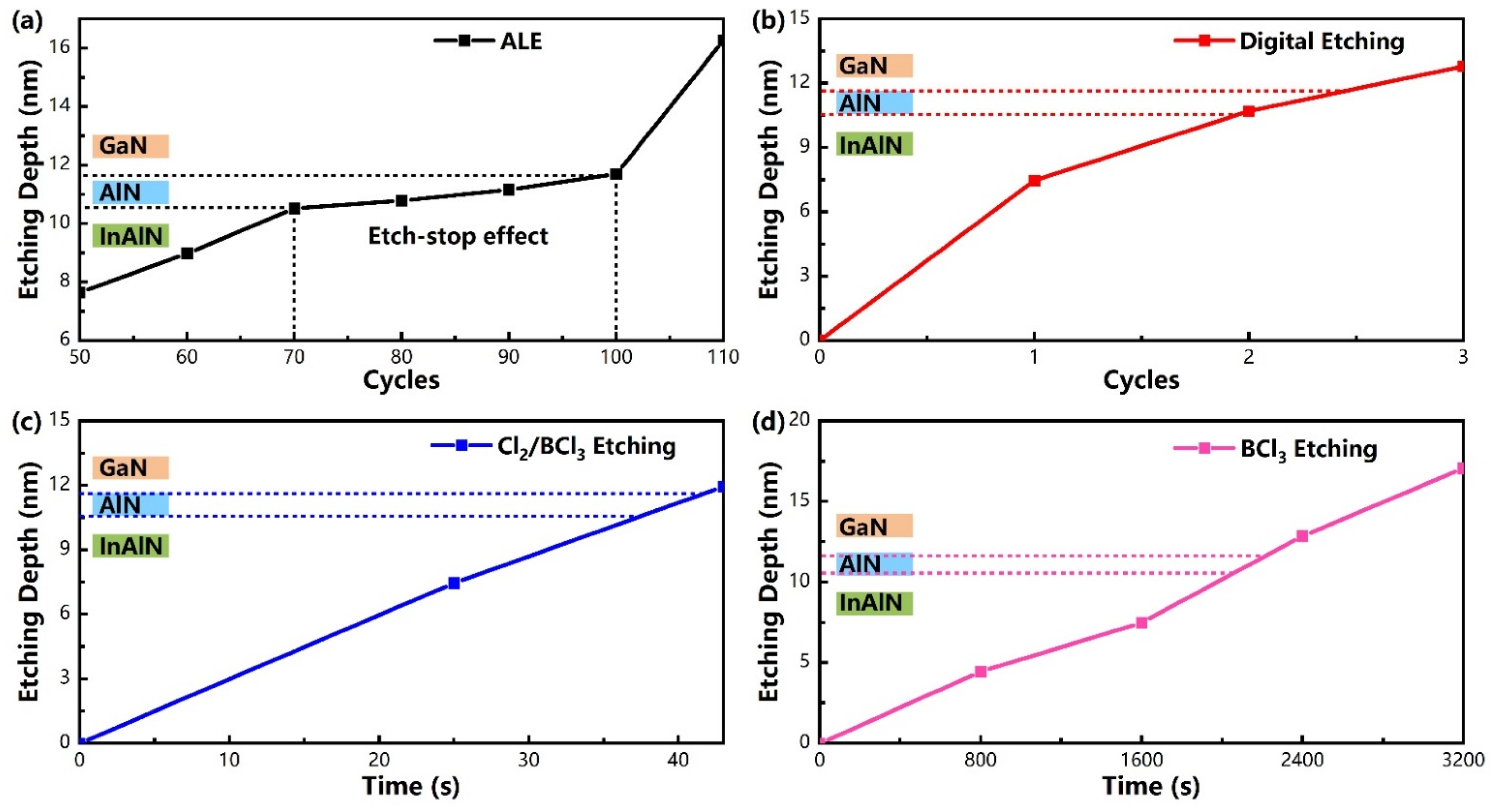
Figure 1. (a) Cross section schematic, (b) scanning transmission electron microscopy (STEM) image and (c) partially enlarged STEM image of In0.17Al0.83N/GaN wafer.
Crystals 12 00722 g001
Figure 2. Cross section schematic of InAlN/GaN samples during atomic layer etching (ALE) process: (a1) SiO2 hard mask deposition, (a2) O2 modification step, (a3) BCl3 removal step, and (a4) removal of SiO2 hard mask by buffered oxide etch (BOE). Digital etching process: (b1) SiO2 hard mask deposition, (b2) O2 plasma oxidation step, (b3) removal of the oxidation layer by diluted HCl solution, and (b4) removal of SiO2 hard mask by BOE. Continuous etching process: (c1) SiO2 hard mask deposition, (c2) Cl2/BCl3 or BCl3 plasma continuous etching, and (c3) removal of SiO2 hard mask by BOE.
Crystals 12 00722 g002
Figure 3. (a) Etching per cycle (EPC) and InAlN root mean square (RMS) roughness with various O2 modification times for ALE technique, (b) etching depth of InAlN (11.6 nm)/GaN wafer for ALE technique (O2 modification time = 30 s) during 0–100 etching cycles, and InAlN EPC dispersion of ALE technique.
Crystals 12 00722 g003
Figure 4. Etching depth vs. etching cycles for (a) ALE (sample S1), (b) digital etching (sample S2), and etching depth vs. etching times for (c) Cl2/BCl3 continuous etching (sample S3) and (d) BCl3 continuous etching (sample S4).
Crystals 12 00722 g004
Figure 5. AFM images (5 × 5 μm2) for InAlN as-grown surface of (a) sample S0; InAlN etched surface of (b) sample S1, (c) sample S2, (d) sample S3 and (e) sample S4; AlN etched surface of (f) sample S1; and the dispersion of InAlN RMS roughness for (g) sample S1 and (h) sample S2.
Crystals 12 00722 g005
Figure 6. The X-ray photoelectron spectroscopy (XPS) measurements of the oxides on the InAlN surface during the whole process of one cycle of ALE: (a) Al2O3 content and (b) In2O3 content of as-grown sample S0 exposed to air, sample S1 after O2 modification step then sealing in vacuum, and sample S1 after one cycle of ALE then sealing in vacuum.
Crystals 12 00722 g006
Figure 7. Epitaxy property measurements of sample S0 with (a) STEM and (bd) energy dispersive X-ray spectroscopy (EDS) measurements.
Crystals 12 00722 g007
Figure 8. Resistor Hall effect (Hall) measurements of samples with 0–5 cycles of ALE surface treatment followed by rapid thermal annealing (RTA): (a) Rsh, (b) 2-DEG mobility and density.
Crystals 12 00722 g008
Table 1. The EPC and etching rate of the InAlN, AlN and GaN layers for samples S1–4.
Etching MethodInAlN Etching RateAlN Etching RateGaN Etching Rate
Sample S10.15 nm/cycle (EPC)0.03 nm/cycle (EPC)0.46 nm/cycle (EPC)
Sample S27.46 nm/cycle (EPC)-1-1
Sample S317.88 nm/min-1-1
Sample S40.28 nm/min-10.32 nm/min
1 Due to the fact that these samples will be directly etched through the InAlN/GaN layer, the partial etching rate could not be calculated for samples S2–4.
Table 2. The surface roughness for InAlN surface of samples S0–4 and AlN etched surface of sample S1.
Etching MethodRMS Roughness (nm)Mean Roughness (nm)
Sample S00.710.47
Sample S10.610.44
Sample S20.690.47
Sample S30.910.75
Sample S40.890.66
Sample S1_AlN0.600.45
Table 3. The 5 × 5 μm2 RMS roughness and electrical properties of samples with 0–5 cycles of ALE surface treatment followed by RTA.
Surface Treatment MethodRMS Roughness (nm)Rsh (Ω/sq)2-DEG Mobility (cm2·V−1·s)2-DEG Density (×1013 cm−2)
Sample S00.4438612101.33
1 cycle sample S10.564549541.44
2 cycles sample S10.4744010001.41
3 cycles sample S10.4540110301.51
4 cycles sample S10.3936011501.50
5 cycles sample S10.4036311201.53
Publisher’s Note: MDPI stays neutral with regard to jurisdictional claims in published maps and institutional affiliations.

