
Channel Mobility Model of Nano-Node MOSFETs Incorporating Drain-and-Gate Electric Fields


Abstract
1. Introduction
2. Experimental and Mobility Fitting
3. Results
4. Discussion
5. Conclusions
Author Contributions
Funding
Institutional Review Board Statement
Informed Consent Statement
Data Availability Statement
Acknowledgments
Conflicts of Interest
References
- Streetman, B.G.; Banerjee, S.K. Solid State Electronic Devices, 7th ed.; Pearson: Hoboken, NJ, USA, 2016; pp. 290–350. [Google Scholar]
- Hu, C. Modern Semiconductor Devices for Integrated Circuits, 1st ed.; Pearson: Hoboken, NJ, USA, 2010; pp. 213–265. [Google Scholar]
- Nguyen-Duc, C.; Cristoloveanu, S.; Ghibaudo, G. A three-piece model of channel length modulation in submicrometer MOSFETs. Solid-State Electron. 1988, 31, 1057–1063. [Google Scholar] [CrossRef]
- Lim, K.Y.; Zhou, X. An analytical effective channel-length modulation model for velocity overshoot in submicron MOSFETs based on energy-balance formulation. Microelectron. Reliab. 2002, 42, 1857–1864. [Google Scholar] [CrossRef]
- Moon, B.J.; Park, C.K.; Lee, K.; Shur, M. New short-channel n-MOSFET current-voltage model in strong inversion and unified parameter extraction method. IEEE Trans. Electron. Dev. 1991, 38, 592–602. [Google Scholar] [CrossRef]
- Shasidl, G.G.; Antoniadis, D.A.; Smith, H.I. Electron velocity overshoot at room and liquid nitrogen temperatures in silicon inversion layers. IEEE Electron. Dev. Lett. 1988, 9, 94–96. [Google Scholar]
- Thornber, K.K. Current equations for velocity overshoot. IEEE Electron. Dev. Lett. 1982, 3, 69–71. [Google Scholar] [CrossRef]
- Kobayashi, T.; Saito, K. Two-dimensional analysis of velocity overshoot effects in ultrashort-channel Si MOSFET’s. IEEE Trans. Electron. Dev. 1985, 32, 788–792. [Google Scholar] [CrossRef]
- Chou, S.Y.; Antoniadis, D.A.; Smith, H.I. Observation of electron velocity overshoot in sub-100-nm-channel MOSFET’s in silicon. IEEE Electron. Dev. Lett. 1985, 6, 665–667. [Google Scholar] [CrossRef]
- Chamberlain, S.G.; Husain, A.; Gaensslen, F.H. Nonuniform displacement of MOSFET channel pinchoff. IEEE Trans. Electron. Dev. 1984, 31, 252–256. [Google Scholar] [CrossRef]
- Huang, H.S.; Wang, W.L.; Wang, M.C.; Chao, Y.H.; Wang, S.J.; Chen, S.Y. I-V model of nano nMOSFETs incorporating drift and diffusion current. Vacuum 2018, 155, 76–82. [Google Scholar] [CrossRef]
- Tachiki, K.; Ono, T.; Kobayashi, T.; Kimoto, T. Short-channel effects in SiC MOSFETs based on analyses of saturation drain current. IEEE Trans. Electron. Dev. 2021, 68, 1382–1384. [Google Scholar] [CrossRef]
- Unleashing the Future of Innovation. Available online: https://research.tsmc.com/assets/download/Chairman_2021_ISSCC.pdf (accessed on 20 May 2021).
- MBCFET—Multi-Bridge Channel FET. Available online: https://samsungatfirst.com/mbcfet/ (accessed on 20 June 2021).
- Intel Introduces New RibbonFET and PowerVia Technologies. Available online: https://www.youtube.com/watch?v=Rt-7c9Wgnds/ (accessed on 27 July 2021).
- Seon, Y.; Chang, J.; Yoo, C.; Jeon, J. Device and Circuit Exploration of Multi-Nanosheet Transistor for Sub-3 nm Technology Node. Electronics 2021, 10, 180. [Google Scholar] [CrossRef]
- Lee, J.C.; Cho, H.J.; Kang, C.S.; Rhee, S.; Kim, Y.H.; Choi, R.; Kang, C.Y.; Choi, C.; Abkar, M. High-k dielectrics and MOSFET characteristics. In Proceedings of the IEEE International Electron Devices Meeting, Washington, DC, USA, 8–10 December 2003. [Google Scholar] [CrossRef]
- Liao, J.C.; Chang, T.C.; Syong, W.R.; Lu, Y.H.; Liu, H.W.; Lin, C.Y.; Ciou, F.M.; Lin, Y.S. The impact of different TiN capping metal thicknesses on high-k oxygen vacancies in n-MOSFETs. IEEE Trans. Dev. Mater. Reliab. 2017, 17, 799–801. [Google Scholar] [CrossRef]
- Na, S.; Yoon, S. Impacts of HfO2/ZnO stack-structured charge-trap layers controlled by atomic layer deposition on nonvolatile memory characteristics of In-Ga-Zn-O channel charge-trap memory thin-film transistors. IEEE J. Electron Dev. Soc. 2019, 7, 453–461. [Google Scholar] [CrossRef]
- Ryu, D.; Kim, M.; Yu, J.; Kim, S.; Lee, J.; Park, B. Investigation of sidewall high-k interfacial layer effect in gate-all-around structure. IEEE Trans. Electron. Dev. 2020, 67, 1859–1863. [Google Scholar] [CrossRef]
- Austin, D.Z.; Allman, D.; Price, D.; Hose, S.; Conley, J.F. Plasma enhanced atomic layer deposition of Al2O3/SiO2 MIM capacitors. IEEE Electron. Dev. Lett. 2015, 36, 496–498. [Google Scholar] [CrossRef]
- Zouw, K.; Aarnink, A.A.I.; Schmitz, J.; Kovalgin, A.Y. Conduction and electric field effect in ultra-thin tungsten films. IEEE Trans. Semicond. Manufact. 2020, 33, 202–209. [Google Scholar] [CrossRef]
- Lin, Y.C.; Chung, V.P.J.; Santhanam, S.; Mukherjee, T.; Fedder, G.K. Sidewall metallization on CMOS MEMS by platinum ALD patterning. J. Microelectromech. Syst. 2020, 29, 978–983. [Google Scholar] [CrossRef]
- Hou, Y.T.; Li, M.F.; Low, T.; Kwong, D.L. Metal gate work function engineering on gate leakage of MOSFETs. IEEE Trans. Electron. Dev. 2004, 51, 1783–1789. [Google Scholar] [CrossRef]
- Huang, A.; Zheng, X.; Xiao, Z. Interface dipole engineering in metal gate/high-k stacks. Chin. Sci. Bull. 2012, 57, 2872–2878. [Google Scholar] [CrossRef]
- Foty, D. MOSFET Modeling with SPICE Principles and Practice, 1st ed.; Prentice Hall: Upper Saddle River, NJ, USA, 1997. [Google Scholar]
- Xiao, H. Introduction to Semiconductor Manufacturing Technology, 2nd ed.; SPIE: Bellingham, DC, USA, 2012. [Google Scholar]
- Murnal, V.R.; Vijaya, C. A quasi-ballistic drain current, charge and capacitance model with positional carrier scattering dependency valid for symmetric DG MOSFETs in nanoscale regime. Nano Converg. 2019, 6, 19. [Google Scholar] [CrossRef] [PubMed]
- Wojcik, D.K.; Dorfman, J.R. Crossover from diffusive to ballistic transport in periodic quantum maps. Phys. D Nonlinear Phenom. 2004, 187, 223–243. [Google Scholar] [CrossRef][Green Version]
- Convertino, C.; Zota, C.B.; Caimi, D.; Sousa, M.; Moselund, K.E.; Czornomaz, L. High-performance InGaAs FinFETs with raised source/drain extensions. Jpn. J. Appl. Phys. 2019, 58, 080901. [Google Scholar] [CrossRef]
- Chen, M.L.; Sun, X.; Liu, H.; Wang, H.; Zhu, Q.; Wang, S.; Du, H.; Dong, B.; Zhang, J.; Sun, Y.; et al. A FinFET with one atomic layer channel. Nat. Comm. 2020, 11, 1205. [Google Scholar] [CrossRef] [PubMed]
- Zhang, S. Review of modern field effect transistor technologies for scaling. J. Phys. Conf. Ser. 2020, 1617, 012054. [Google Scholar] [CrossRef]
- Kim, S.; Kim, M.; Ryu, D.; Lee, K.; Kim, S.; Lee, J.; Lee, R.; Kim, S.; Lee, J.H.; Park, B.G. Investigation of electrical characteristic behavior induced by channel-release process in stacked nanosheet gate-all-around MOSFETs. IEEE Trans. Electron Dev. 2020, 67, 2648–2652. [Google Scholar] [CrossRef]
- Park, C.; Yun, I. Degradation of off-phase leakage current of FinFETs and gate-all-around FETs induced by the self-heating effect in the high-frequency operation regime. IEEE Trans. Nanotechnol. 2020, 19, 308–314. [Google Scholar] [CrossRef]
- Bao, R.; Watanabe, K.; Zhang, J.; Guo, J.; Zhou, H.; Gaul, A.; Sankarapandian, M.; Li, J.; Hubbard, A.R.; Vega, R.; et al. Multiple-Vt solutions in nanosheet technology for high performance and low power applications. In Proceedings of the IEEE International Electron Devices Meeting, San Francisco, CA, USA, 7–11 December 2019. [Google Scholar] [CrossRef]
- Yoon, J.S.; Jeong, J.; Lee, S.; Baek, R.H. Optimization of nanosheet number and width of multi-stacked nanosheet FETs for sub-7-nm node system on chip applications. Jpn. J. Appl. Phys. 2019, 58, BA12. [Google Scholar] [CrossRef]
- The Nanosheet Transistor Is the Next (and Maybe Last) Step in Moore’s Law. Available online: https://spectrum.ieee.org/the-nanosheet-transistor-is-the-next-and-maybe-last-step-in-moores-law (accessed on 26 July 2021).
- Rama Krishna, M.V.; Friesner, R.A. Quantum confinement effects in semiconductor clusters. J. Chem. Phys. 1991, 95, 8309. [Google Scholar] [CrossRef]
- Borrelli, N.F.; Hall, D.W.; Holland, H.J.; Smith, D.W. Quantum confinement effects of semiconducting microcrystallites in glass. J. Appl. Phys. 1987, 61, 5399. [Google Scholar] [CrossRef]
- Norris, D.J.; Bawendi, M.G. Measurement and assignment of the size-dependent optical spectrum in CdSe quantum dots. Phys. Rev. B 1996, 53, 16338–16346. [Google Scholar] [CrossRef]
- Mushonga, P.; Onani, M.O.; Madiehe, A.M.; Meyer, M. Indium phosphide-based semiconductor nanocrystals and their applications. J. Nanomater. 2012, 2012, 869284. [Google Scholar] [CrossRef]
- Cheng, C.K.; Ho, C.T.; Lee, D.; Lin, B.; Park, D. Complementary-FET (CFET) standard cell synthesis framework for design and system technology co-optimization using SMT. IEEE Trans. VLSI Syst. 2021, 29, 1178–1191. [Google Scholar] [CrossRef]
- Vincent, B.; Boemmels, J.; Ryckaert, J.; Ervin, J. A benchmark study of complementary-field effect transistor (CFET) process integration options done by virtual fabrication. IEEE J. Electron. Dev. Soc. 2020, 8, 668–673. [Google Scholar] [CrossRef]
- Gupta, M.K.; Weckx, P.; Schuddinck, P.; Jang, D.; Chehab, B.; Cosemans, S.; Ryckaert, J.; Dehaene, W. The complementary FET (CFET) 6T-SRAM. IEEE Trans. Electron. Dev. 2021, 68, 6106–6111. [Google Scholar] [CrossRef]


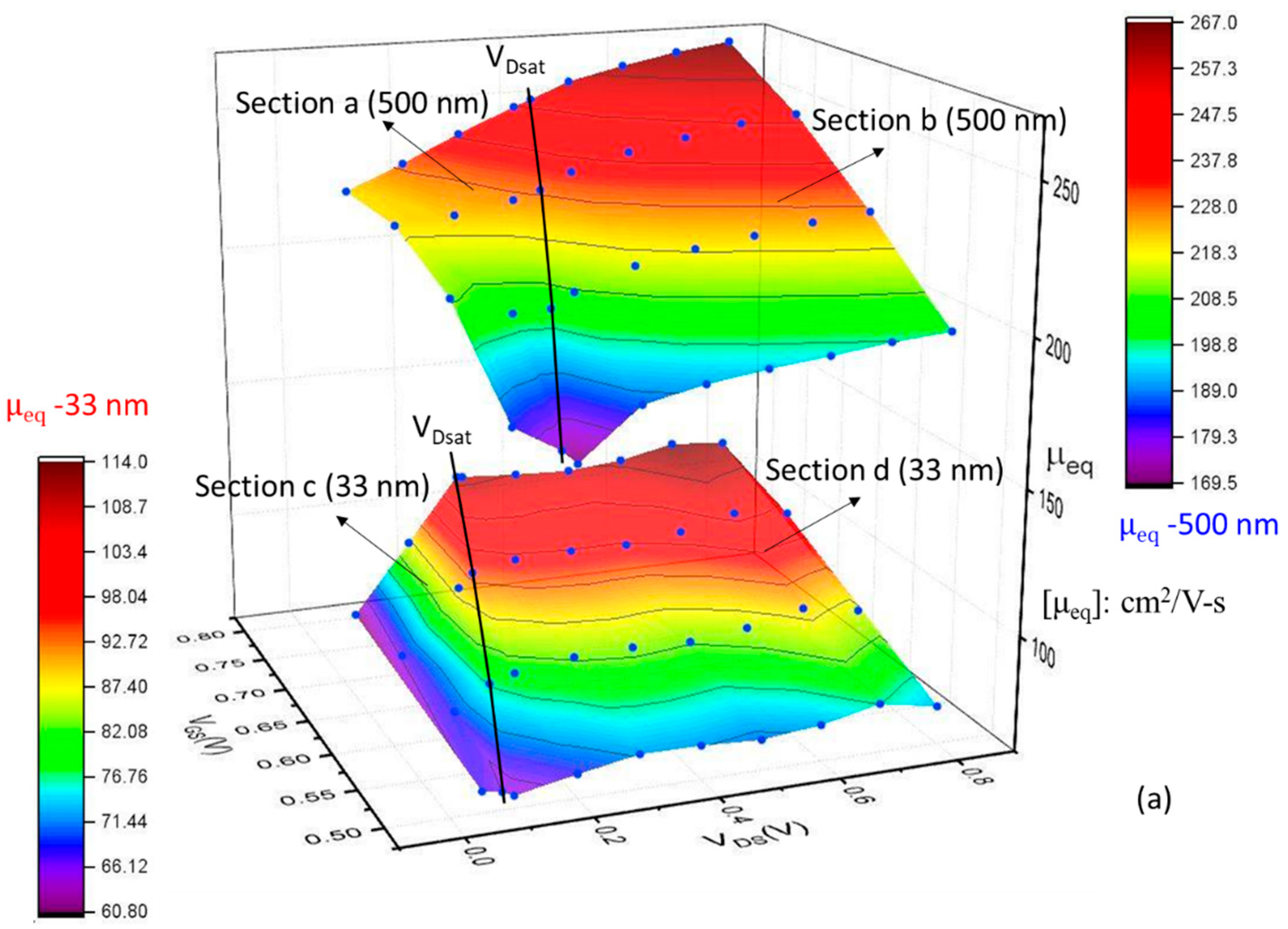
| Channel Length | Operation Mode | Section |
|---|---|---|
| Long (>120 nm) | Linear region | X = a |
| Long (>120 nm) | Saturation region | X = b |
| Short (<120 nm) | Linear region | X = c |
| Short (<120 nm) | Saturation region | X = d |
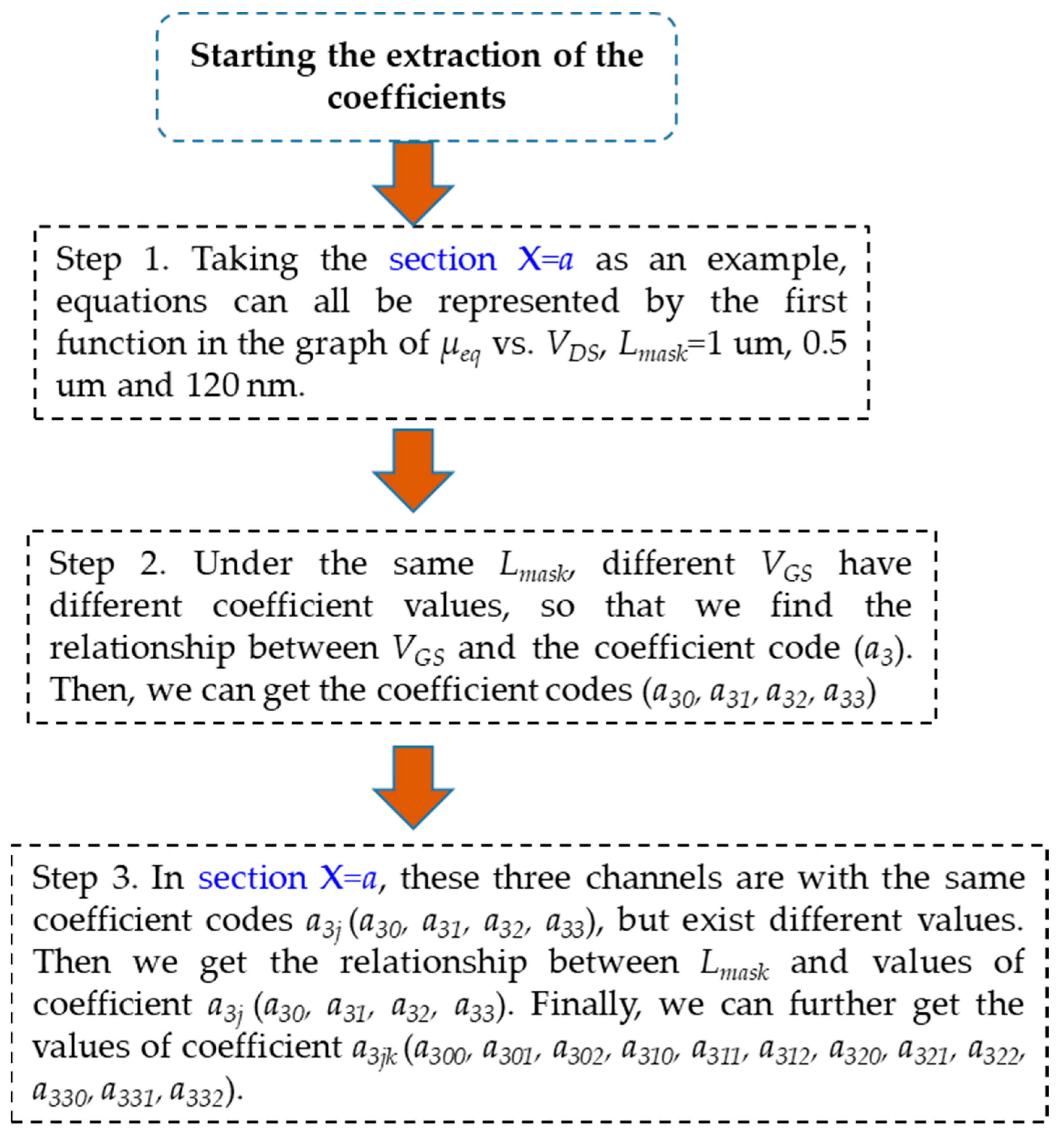
| Coefficient Type | Variables Xi, Xij, and Xijk | Index Range |
|---|---|---|
| μeq (VDS) | Xi: functions of VGS | i = 0, 1, 2, 3 |
| Xi (VGS) | Xij: functions of Lmask | j = 0, 1, 2, 3 |
| Xij (Lmask) | Xijk: fitted constant | k = 0, 1, 2 |
| Coefficient Value | Extracted Sub-Coefficients |
|---|---|
| The value of a3 | a3 = −247.999 |
| The values of a3j | a33 = 19,833.33 |
| a32 = −5150 | |
| a31 = −29,383.3 | |
| a30 = 16,400 | |
| The values of a3jk | a332 = −3,283,858.592 |
| a331 = 5,452,922.151 | |
| a330 = −1,885,663.094 | |
| a322 = 6,422,679 | |
| a321 = −10,725,100.45 | |
| a320 = 3,751,730.477 | |
| a312 = −4,094,362.073 | |
| a311 = 6,889,789.134 | |
| a310 = −2,450,687.382 | |
| a302 = 840,872.7189 | |
| a301 = −1,430,708.191 | |
| a300 = 521,535.9158 |
| Lmask | VT_lin (V) | VT_sat (V) | DIBL (mV/V) |
|---|---|---|---|
| 1 μm | 0.296 | 0.271 | 33.36 |
| 500 nm | 0.307 | 0.277 | 39.01 |
| 120 nm | 0.332 | 0.298 | 46.12 |
| 90 nm | 0.353 | 0.306 | 62.87 |
| 50 nm | 0.395 | 0.305 | 120.38 |
| 33 nm | 0.384 | 0.228 | 208.09 |
Publisher’s Note: MDPI stays neutral with regard to jurisdictional claims in published maps and institutional affiliations. |
© 2022 by the authors. Licensee MDPI, Basel, Switzerland. This article is an open access article distributed under the terms and conditions of the Creative Commons Attribution (CC BY) license (https://creativecommons.org/licenses/by/4.0/).
Share and Cite
Chao, S.-Y.; Huang, H.-S.; Huang, P.-R.; Lin, C.-Y.; Wang, M.-C. Channel Mobility Model of Nano-Node MOSFETs Incorporating Drain-and-Gate Electric Fields. Crystals 2022, 12, 295. https://doi.org/10.3390/cryst12020295
Chao S-Y, Huang H-S, Huang P-R, Lin C-Y, Wang M-C. Channel Mobility Model of Nano-Node MOSFETs Incorporating Drain-and-Gate Electric Fields. Crystals. 2022; 12(2):295. https://doi.org/10.3390/cryst12020295
Chicago/Turabian StyleChao, Shou-Yen, Heng-Sheng Huang, Ping-Ray Huang, Chun-Yeon Lin, and Mu-Chun Wang. 2022. "Channel Mobility Model of Nano-Node MOSFETs Incorporating Drain-and-Gate Electric Fields" Crystals 12, no. 2: 295. https://doi.org/10.3390/cryst12020295
APA StyleChao, S.-Y., Huang, H.-S., Huang, P.-R., Lin, C.-Y., & Wang, M.-C. (2022). Channel Mobility Model of Nano-Node MOSFETs Incorporating Drain-and-Gate Electric Fields. Crystals, 12(2), 295. https://doi.org/10.3390/cryst12020295