Article

Reliability of SnPbSb/Cu Solder Joint in the High-Temperature Application

1
College of Electrical Engineering, Nanjing Vocational University of Industry Technology, Nanjing 210023, China
2
College of Mechanical & Electrical Engineering, Nanjing University of Aeronautics and Astronautics, Nanjing 210001, China
3
Jinhua Sanhuan Welding Materials Company Limited, Jinhua 321000, China
4
College of Materials Science and Technology, Nanjing University of Aeronautics and Astronautics, Nanjing 210001, China
*
Authors to whom correspondence should be addressed.
Crystals 2022, 12(12), 1724; https://doi.org/10.3390/cryst12121724
Submission received: 27 October 2022 / Revised: 21 November 2022 / Accepted: 23 November 2022 / Published: 28 November 2022
(This article belongs to the Special Issue Physical Mechanism of Welding of Metallic Materials)

Abstract

:
With the continuous miniaturization and increase in functionality of the electronic devices used in the aerospace and national defense industries, the requirements for reliability of the solder joints in these devices keep increasing. In this study, a SnPbSb solder with excellent wettability was used as the research object, and the effects of high-temperature aging at 150 °C on the microstructure and mechanical properties of SnPbSb/Cu solder joints were investigated according to the relevant industry standards. It was found that high-temperature aging does not change the eutectic structure of the SnPbSb solder, but it does significantly coarsen the Sn-rich phase and the Pb-rich phase in the solder. In addition, the interfacial intermetallic compound (IMC) layer in the SnPbSb/Cu solder joint changes from a Cu6Sn5 single layer to a Cu6Sn5/Cu3Sn double layer after the aging, and the thickness of the IMC layer increases greatly. High-temperature aging significantly deteriorates the mechanical properties of the solder joints. After aging at 150 °C for 1000 h, the shear strength of the SnPbSb/Cu solder joints decreased by 45.39%, while the ductile fracture mode did not change.

1. Introduction

In recent years, the performances of electronic devices in the fields of national defense, aerospace and civil products have received more and more attention and have become a hot area of international competition. Electronic components are the basis of these electronic devices. The separated electronic components should be connected through soldering to form electrical–mechanical connections and further assembled into functional electronic devices. Because soldering is one of the major joining methods in the packaging of electronic devices, the quality of solder joints significantly affects the reliability of the electronic devices. At present, the commonly used solders in electronic packaging can be mainly divided into Pb-containing solder, represented by SnPb37 alloy, and Pb-free solders such as SnAgCu and SnBi alloys [1]. The SnPb37 alloy is a traditional solder alloy in the electronics industry which was widely used in the packaging of commercial electronic products. Containing the Pb element, the SnPb37 solder has excellent wettability. With the Pb-free trend in the commercial electronics industry since 2000, a series of Pb-free solders have been proposed, but the wettability of the existing commercial Pb-free solders is still much lower than that of the SnPb solders, which restricts the application of the Pb-free solders [2]. As the aerospace and national defense industries are not limited by the Pb-free requirement, the SnPb solders are still widely used in these industries [3].
Traditional electronic packaging mainly integrates the components onto circuit boards by surface mounting and through-hole insertion methods, i.e., in a two-dimensional planar packaging method. With the continuous development of electronic technology, the packaging has changed into three-dimensional packaging, and the sizes of the electronic components as well as the solder joints have decreased significantly. However, the decrease in size of the solder joint puts higher requirements on the wettability of the solder alloy because the solder must be able to spread well on smaller pads to form separated joints with no bridging, avoiding the short failures of integrated circuits. Therefore, the SnPb solder with excellent wettability can better meet the requirements of small-sized solder joints compared with the Pb-free solders, and it has broad application prospects in the packaging of advanced electronic systems in the aerospace and national defense industries [4]. Moreover, due to the significant improvements in the integration and power of electronic devices, heat dissipation is increasingly difficult, which leads to the service temperature of the solder joints increasing [5]. Previous studies have shown that long-term exposure to a high-temperature environment significantly deteriorates the mechanical properties of solder joints and increases the risk of premature fracture failure [6]. Under the miniaturization and high-power trends of electronic devices in the future, the reliability of the solder joints will become more prominent. Therefore, high-temperature aging is usually used to evaluate the reliability of solder joints in current studies of soldering for electronic packaging, and the aging temperature is usually set to be 125~150 °C in the related industry standards.
Among the SnPb solders, the SnPb37 eutectic solder is the most widely used due to its low melting point. The SnPb50 solder has a higher liquidus temperature and excellent wettability and cryogenic performance, meaning it has a longer service life in a variety of complex environments, and thus it is also widely used in the fields of aerospace and national defense industries. A recent study [7] reveals that adding a small amount of Sb can significantly improve the reliability of a solder, and a significant improvement effect can be achieved with 1.0 wt % of Sb addition, while an excessive Sb addition will embrittle the solder. For the SnPbSb solder, investigations reveal that thermal cycling of −65~150 °C not only increases the thickness of the intermetallic compound (IMC) layer at the joint interface, but also decreases the strength of the SnPbSb/Cu solder joint, while the thermal shock at −196~150 °C will result in microcracks at the SnPbSb/Cu joint interface and deteriorate the performance of the solder joints [4,8]. Therefore, it can be considered that the SnPbSb/Cu solder joint is sensitive to its service environment, and it is necessary to clarify the influences of service environments on the microstructure and properties of the SnPbSb/Cu solder joints to ensure the reliable application of the SnPbSb solder. However, the existing research on the reliability of the SnPbSb solder focuses mainly on the temperature cycle, while reports on high-temperature aging of the SnPbSb solder are lacking. To evaluate the reliability of the SnPbSb under relatively high temperature and meet the needs of the aerospace and national defense industries in the future, in this study an aging temperature of 150 °C was chosen according to the relevant electronic industry standards. The changes in the solder matrix and interfacial microstructure of the SnPbSb/Cu solder joint during the long-term aging process, as well as the resulting evolution of its mechanical properties, were investigated. It is hoped that this study can provide a reference for the future application of the SnPbSb solder in advanced electronic devices and a basis for the development of advanced soldering materials.

2. Materials and Methods

The SnPb49Sb1 (wt %) solder alloy (hereinafter referred to as SnPbSb solder) was prepared by smelting Sn, Pb and Sb with a purity of 99.99 wt % in a vacuum furnace. The smelting temperature was 670 °C, and the vacuum degree was 1 × 10² Pa. Analysis of the obtained SnPbSb solder by a spectrometer (SpectroMAXx) revealed that its composition was very close to the design composition, as listed in Table 1. The obtained SnPbSb solder was cut and soldered onto Cu at 250 °C for 2 min to prepare the SnPbSb/Cu solder joint sample. According to the National Military Standard of the People’s Republic of China (GJB 548B-2005, Test Methods and Procedures for Microelectronic Devices), the prepared samples were aged in an oil bath at 150 °C for 0~1000 h, and the microstructure and mechanical properties of the samples aged for different times were characterized.
A scanning electron microscope (SEM) and an energy-dispersive spectrometer (EDS) were used to observe the microstructure and analyze the chemical composition of the solder joint samples. The Image Pro Plus software was used to calculate the average area of the Pb-rich phase (APb) in the SEM images of the solder, so as to characterize the coarsening behavior of the SnPbSb solder matrix during high-temperature aging. The calculation equation is as follows:
APb = SPb/n
in which SPb is the total area of the Pb-rich phase in the SEM image, and n is the total number of the Pb-rich phase.
The average thickness of the interfacial IMC layer (dIMC) in the solder joints was also calculated with the same software to reveal the interfacial behavior during the aging process. The thickness of the interfacial IMC layer is calculated as follows:
dIMC = Si/li
where Si is the total area of the IMC layer in the SEM image, and li is the length of the joint interface.
Additionally, to further reveal the morphology of the interfacial IMC layer, a nitric acid alcohol solution was used to remove the solder of some joint samples to expose the interface IMC grains, and the changes in the interfacial microstructure of the solder joints were characterized more accurately combined with the cross-sectional morphology. The corrosion method has been introduced in the literature [8].
The mechanical properties of the solder joints were tested by an STR-1000 micro-solder joint tester. As shown in Figure 1, the 0805 chip resistors were soldered onto the printed circuit board with the prepared solder. Before the test, the shear instrument of the tester was placed at a location 2 mm in front of the center of the chip resistor, and then the shear pusher was pushed at a constant speed of 1 mm/min along the set shear direction until the solder joint was broken. The maximum force during the test process is recorded as the shear force of the solder joint, which is converted into the shear strength by dividing by the joint area. Five samples were tested under the same parameters, and the average value was calculated.

3. Results and Discussion

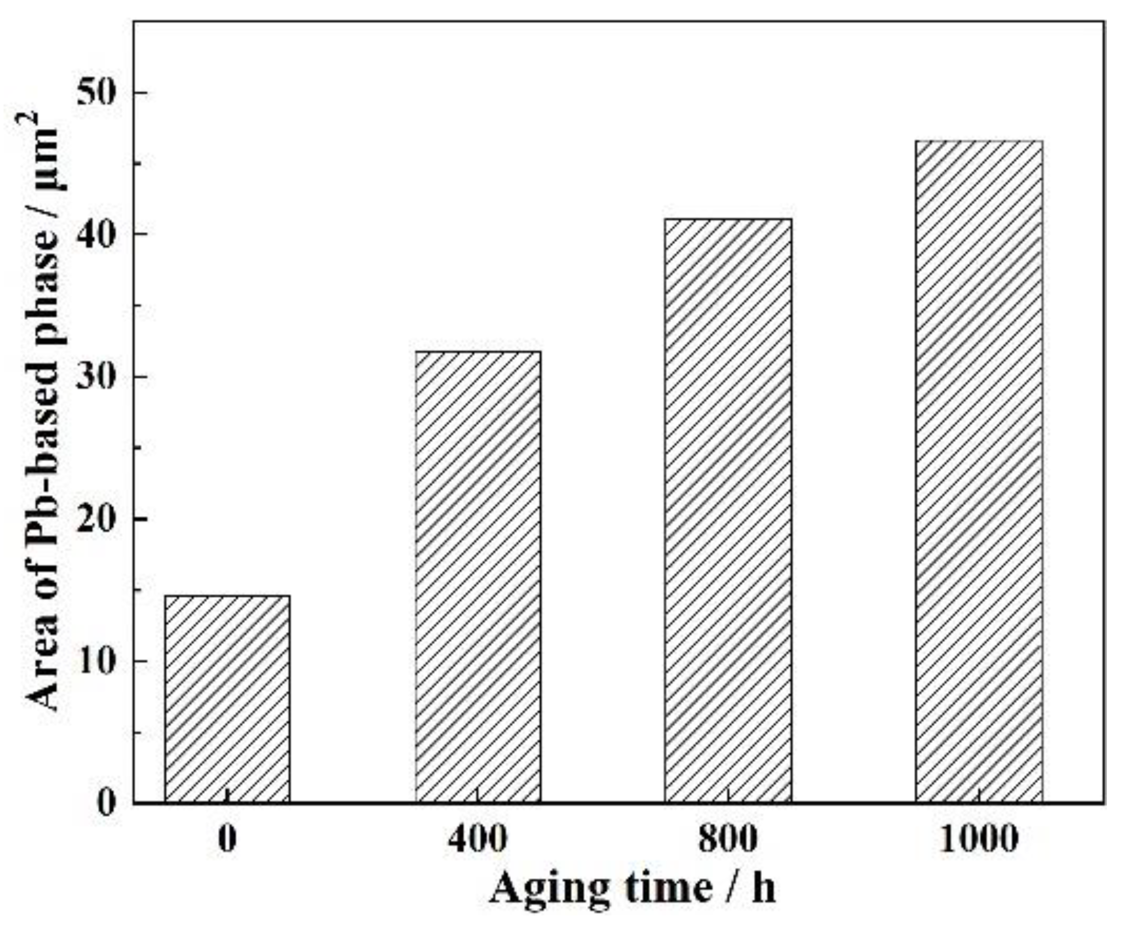
3.1. Evolution in Microstructure of the Solder

The microstructures of the SnPbSb solder in the solder joint aged at 150 °C for different times are shown in Figure 2. It can be seen from Figure 2a that there are two phases in the as-soldered SnPbSb matrix of the joint, i.e., the light-colored Pb-rich phase and the dark colored Sn-rich phase. The two phases were alternately distributed, showing the characteristics of a eutectic structure. As the Sb element was solid-soluble in the Sn-rich phase, no Sb-rich phase was detected. In addition, it could be found that the Pb-rich phase was finer and quite uniform in the as-soldered SnPbSb/Cu solder joint. After aging for 400 h, the eutectic structure hardly changed, while the Pb-rich phase coarsened obviously, as shown in Figure 2b. With a further increase in the aging time, the SnPbSb solder became coarser, while the size of the Pb-rich phase particles became very non-uniform after aging for 1000 h (see Figure 2c,d).
The average areas of the Pb-rich phase in the SnPbSb solders aged for different times are presented in Figure 3. For the solder in the solder joint without aging, it could be found from the image that the area of the Pb-rich phase was only 14.62 μm2. With increasing aging time, the size of the Pb-rich phase increased gradually. After aging for 1000 h, the area of the Pb-rich phase increased to 46.61 μm2, which was 218.81% higher than that before the aging, demonstrating that the coarsening trend of the solder was very significant.
The coarsening process of the Pb-rich phase during the high-temperature aging is related to atomic diffusion, and the relationship between the atomic diffusion coefficient and temperature can be expressed by the following equation [9]:
D = D0 × e(−Q/kT)
in which D0 is the diffusion constant, Q is the diffusion activation energy, and T is the thermodynamic temperature. With increasing aging temperature, the diffusion coefficients of atoms in the SnPbSb solder increased, and hence the diffusion rate was accelerated. The mutual diffusion of the Pb atoms and Sn atoms resulted in continuous growth in the size of the Pb-rich phase and the serious coarsening of the solder.

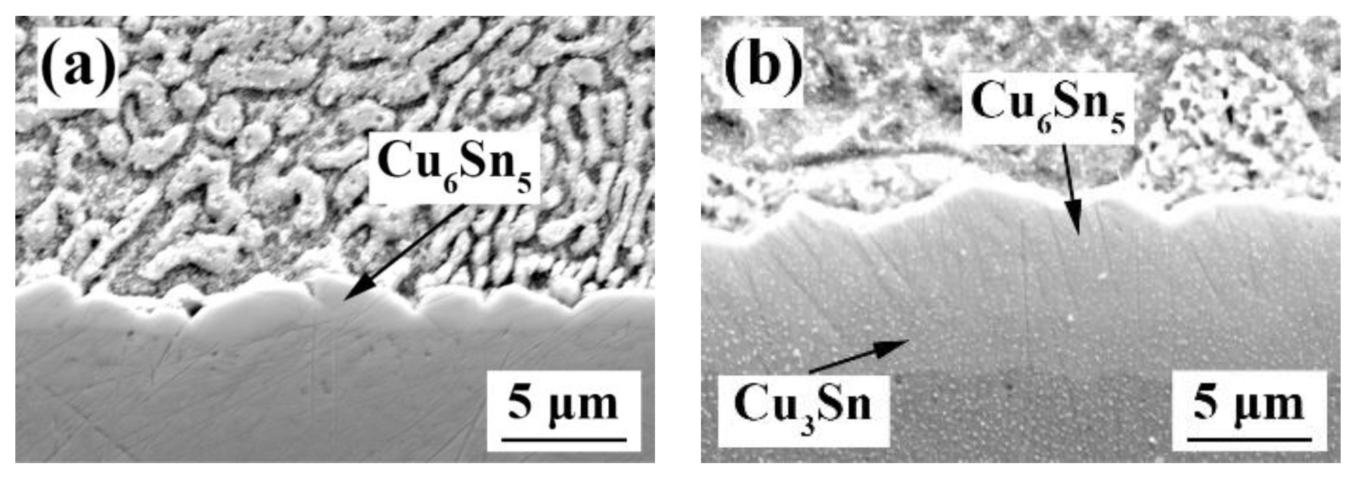
3.2. Evolution in Microstructure of the Joint Interface

The formation of a continuous IMC layer between the Cu substrate and the SnPbSb solder indicates that a metallurgical bond is formed between the solder and the substrate. The microstructure and thickness of the interfacial IMC layer can significantly affect the mechanical properties and reliability of the solder joint. Figure 4 shows the morphologies of the IMC layers at the SnPbSb/Cu interfaces aged at 150 °C for different times. For the as-soldered SnPbSb/Cu interface, a thin Cu6Sn5 layer with a scallop-like morphology was obtained, as shown in Figure 4a. After aging for 400 h, the thickness of the Cu6Sn5 layer increased obviously, showing a flat interface, and a Cu3Sn layer appeared between the Cu6Sn5 and the Cu substrate (see Figure 4b). With the thermal aging’s progress, the Cu6Sn5 and Cu3Sn layers both grew, which resulted in a significant thickness increment of the IMC layers compared to the as-soldered joint, as shown in Figure 4c,d.
During the soldering process, the Cu substrate and Sn atoms in the molten solder reacted, forming a Cu6Sn5 layer at the interface [10]. Due to the short soldering time, the Cu6Sn5 layer in the as-soldered joint was thin. Then, during the subsequent thermal aging process, inter-diffusion between the solder and the substrate occurred, so the Cu6Sn5 layer coarsened [11]. Meanwhile, reaction between the Cu6Sn5 layer and the Cu substrate generated a new Cu3Sn IMC layer between the Cu6Sn5 layer and the Cu substrate. During the long-term thermal aging process, the Cu6Sn5 and Cu3Sn layers grew gradually, resulting in significant coarsening of the interfacial IMC layer.
The thicknesses of the IMC layers in the SnPbSb/Cu solder joints during thermal aging are presented in Table 2. Before the aging, there was only a single Cu6Sn5 layer with an average thickness of 1.31 μm. After aging for 1000 h, the interfacial IMC layer changed into a bilayer structure, including a Cu6Sn5 layer of 6.67 μm in thickness and a Cu3Sn layer of 3.31 μm in thickness. The total thickness of the IMC layer increased by 661.83% compared with that before the high-temperature aging, showing significant coarsening behavior.
Previous investigations have revealed that there is a functional relationship between the thickness of the interfacial IMC layer (Xt) and the service time (t) of the solder joints, which can be expressed by the following interface layer growth equation [12]:
Xt = X0 + (Dt)1/2
where X0 is the thickness of the IMC layer in the as-soldered joint, and D is the growth coefficient of the interfacial IMC layer in the service environment, which is used to quantitatively characterize the interfacial reaction behavior of the solder joint. Using Equation (4) to fit the thicknesses of the IMC layers presented in Table 2, the growth curve shown in Figure 5 was obtained. Therefore, the growth equation of the IMC layer in the SnPbSb/Cu joint during thermal aging can be expressed as:
Xt = 1.06 + 0.259t1/2
Based on Equation (5), the growth coefficient of the IMC layer of the SnPbSb/Cu joint was calculated to be 1.86 × 10⁻¹⁷ m2/s at 150 °C.
Figure 6 shows the top-view morphology evolution of the Cu6Sn5 grains during the aging process. As presented in Figure 6a, the Cu6Sn5 particles of the as-soldered joint were fine, hill-like grains, between which there are obvious gaps. This top-view morphology fit with the scallop-like morphology in Figure 4a. During the aging process, the size of the Cu6Sn5 grains increased, and hence the gaps were filled, making the top-view surface of the IMC layer flatter, which also fit with the cross-section morphology [13]. As the Cu3Sn is located between the Cu6Sn5 and the Cu substrate, it cannot be observed from the top view.
The growth of the IMC layers at the Sn-based solder/Cu interfaces has been proven to be attributable to the thermal diffusion of the Cu atoms from the Cu substrate to the joint interface [12]. It can be found from Figure 6a that there were relatively wide gaps between the Cu6Sn5 grains, and thus there were two paths for migration of the Cu atoms towards the IMC/solder interface, as exhibited in Figure 7. The atoms diffused through path A would make the grains grow vertically to the interface by passing through the entire Cu6Sn5 grain, which was relatively difficult. In contrast, diffusion path B through the grain boundary was shorter and quicker, and thus path B was much easier for the migration of the Cu atoms, making the growth of the Cu6Sn5 induced by diffusion through path B more significant. As a result, the gaps between the Cu6Sn5 grains were filled during the aging process, resulting in the morphology changes shown in Figure 4 and Figure 6.

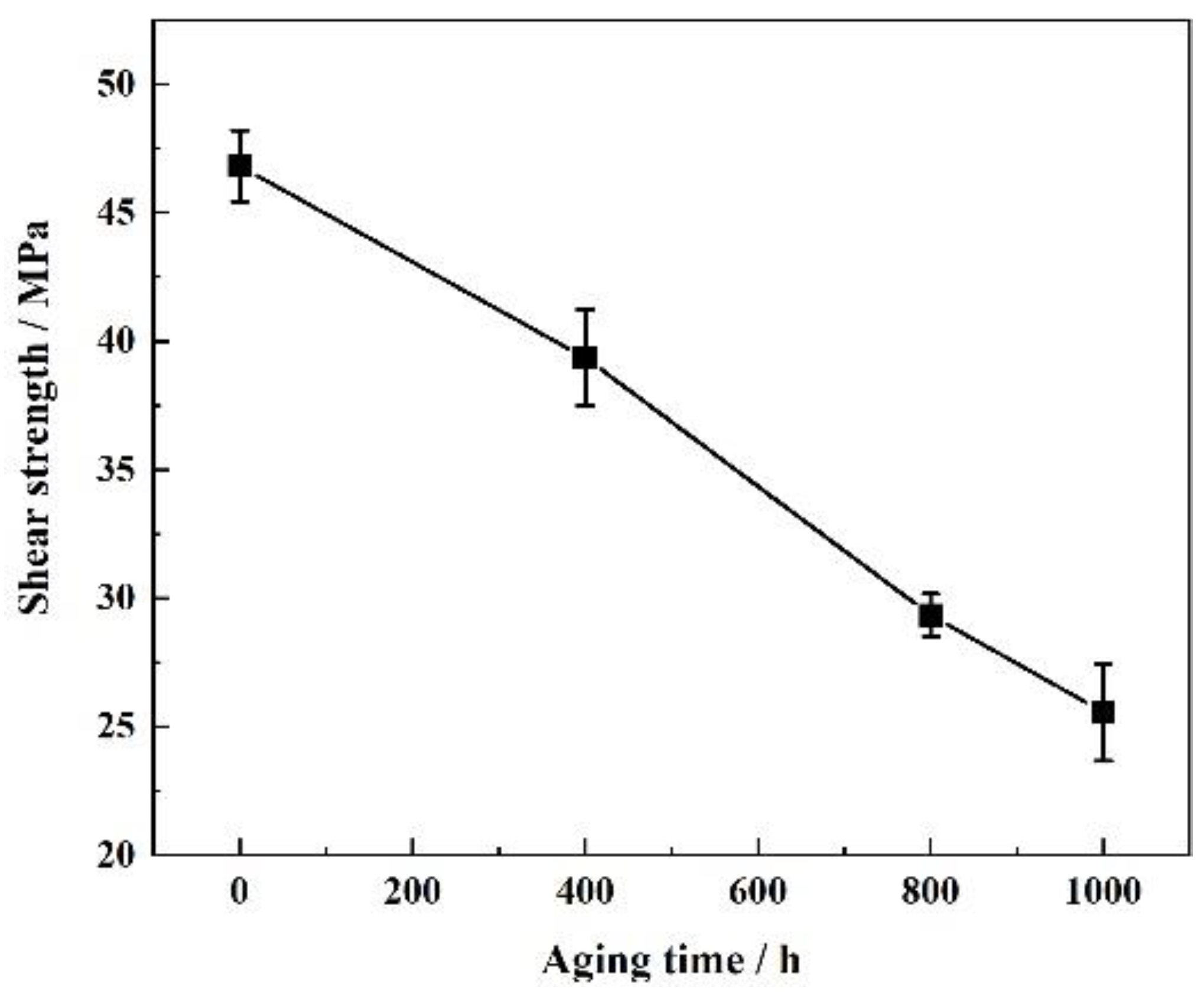
3.3. Shear Strength of the Solder Joint

The shear strength of the SnPbSb/Cu solder joint during the thermal aging process is shown in Figure 8. It can be seen from the figure that the shear strength of the as-soldered SnPbSb/Cu joint reached 46.83 MPa, which indicated that a firm bonding had formed between the SnPbSb solder and the Cu substrate. However, after the thermal aging, the shear strength decreased continuously. After 1000 h of aging, the shear strength of the SnPbSb/Cu solder joint became 25.57 MPa, which was 45.39% lower than that before the aging.
It has been revealed that coarsening the IMC layer significantly worsens the mechanical properties of the solder joint [14,15]. As the intermetallic compounds, the growth of the Cu6Sn5 and Cu3Sn layers increased the brittleness of the solder joint interface, resulting in a higher fracture risk. In addition, the grain boundary can act as an obstacle to crack propagation. The alloy with a finer grain has a higher density of grain boundaries, and thus the obstacle of grain boundaries to fracturing is more obvious, and the mechanical properties of the alloy will be better [16]. During the high-temperature aging process, the thickness of the IMC layer of the SnPbSb/Cu joint increased obviously; meanwhile, the solder matrix coarsened significantly. Due to the combined effect of these two factors, the shear strength of the SnPbSb/Cu solder joint decreased continuously.

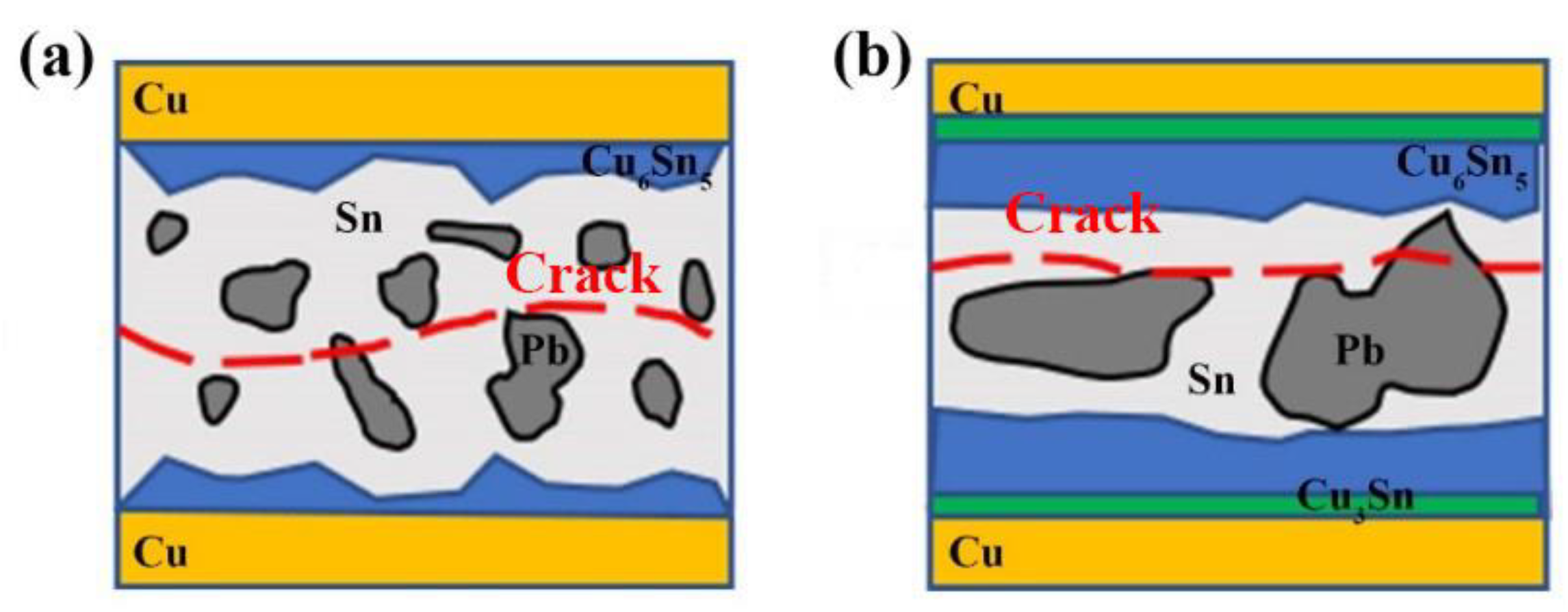
3.4. Fracture Morphologies of the Solder Joints

To further reveal the fracture mechanisms of the SnPbSb/Cu solder joint, the fracture morphologies of the as-soldered and aged solder joints were observed. As shown in Figure 9a, there were a large number of shear dimples on the fracture surface of the as-soldered joint, showing a very obvious ductile fracture characteristic. In addition, the elemental distribution shown in Figure 9b–e demonstrated that almost all the elements on the surface were Sn, Pb and Sb, while Cu was negligible. Hence, it could be predicated that the fracture of the as-soldered SnPbSb/Cu joint is a ductile fracture occurring inside the solder. After aging for 1000 h, shear dimples could still be observed on the fracture surface, whose depth had decreased, but still no brittle fracture feature was observed. The EDS results (see Figure 9g–j) also showed that after aging for 1000 h, the fracture of the solder joint was still a ductile fracture occurring in the solder, but the characteristics of the ductile fracture were not as obvious as in the as-soldered joint, which indicated that the toughness of the solder joint had decreased.
Based on Figure 9, it can be predicated that although the increasing thickness of the interfacial IMC layer during the aging process made the joint interface more brittle, it was not the main reason for the decline in the mechanical properties of the solder joint. Fractures of both the as-soldered and the aged solder joints occurred inside the solder matrix, demonstrating that the worsening of the mechanical properties of the solder joints was closely related to the coarsening of the solder, and its effect was more significant than the coarsening of the interfacial IMC layer. The microstructure of the SnPbSb solder in the solder joint before aging was fine, and the average area of the Pb-rich phase was only 14.62 μm2. After aging for 1000 h, the solder matrix coarsened obviously, and the average area of the Pb-rich phase increased by 218.81%. As illustrated in Figure 10, due to the finer microstructure of the solder matrix, the density of grains before aging was higher, which can not only make plastic deformation occur uniformly in more grains and delay the generation of cracks, but also hinder crack propagation, giving the solder joints a higher strength. After the aging, the grains in the solder matrix coarsened obviously. As a result, the retarding effect of the grain boundary on crack initiation and propagation decreased; meanwhile, the interfacial IMC layer grew significantly, leading to the continuous worsening of the mechanical properties of the solder joints.

4. Conclusions

To examine the reliability of the SnPbSb solder in high-temperature service environment and meet the future requirements of the aerospace and national defense industries for high-wettability solder, the evolutions in the microstructure and mechanical properties of the SnPbSb/Cu solder joints during aging at 150 °C were investigated. The main conclusions are as follows:
(1)
Long-time high-temperature aging promoted the diffusion and migration of atoms, resulting in the continuous coarsening of the SnPbSb solder and the significant increase in size of the Pb-rich phase, while the eutectic structure characteristics were hardly changed.
(2)
The Cu6Sn5 layer grew gradually during the thermal aging process, and the Cu6Sn5/solder interface transformed from a scallop-like morphology into a flat morphology; a Cu3Sn layer appeared between the Cu6Sn5 and the Cu substrate. The thickness of the interfacial IMC layer increased significantly after long-time aging.
(3)
The continuous coarsening of the solder matrix and growth of the IMC layer at the interface co-deteriorated the mechanical properties of the SnPbSb/Cu joint. The shear strength of the SnPbSb/Cu solder joint decreased from 46.83 MPa to 25.57 Mpa after aging for 1000 h.
(4)
During thermal aging, the fracture of SnPbSb/Cu solder joints was always a ductile fracture which occurred in the solder matrix. It could be concluded that the influence of the coarsening solder matrix on the mechanical properties of joints was more significant than that of the growth of the interfacial IMC layer.

Author Contributions

Conceptualization, J.X., Y.F. and S.X.; methodology, J.X. and X.Z.; software, J.X.; validation, J.X.; formal analysis, J.X.; investigation, J.X.; resources, J.X., S.X. and J.Z.; data curation, J.X.; writing—original draft preparation, J.X.; writing—review and editing, J.X.; visualization, J.X.; supervision, Y.F. and S.X.; project administration, J.X. and S.X.; funding acquisition, J.X. All authors have read and agreed to the published version of the manuscript.

Funding

This work was financially supported by Start-up Fund for New Talented Researchers of Nanjing Vocational University of Industry Technology (Grant No.YK21-02-05).

Institutional Review Board Statement

Not applicable.

Informed Consent Statement

Not applicable.

Data Availability Statement

The data can be obtained from the corresponding author.

Conflicts of Interest

The authors declare no conflict of interest.

References

  1. Ma, H.; Suhling, J.C. A review of mechanical properties of lead-free solders for electronic packaging. J. Mater. Sci. 2009, 44, 1141–1158. [Google Scholar] [CrossRef]
  2. Wang, J.H.; Xue, S.B.; Lv, Z.P.; Wang, L.J.; Liu, H. Present Research Status of Lead-free Solder Reinforced by Nanoparticles. Mater. Rep. 2019, 33, 2133–2145. (In Chinese) [Google Scholar]
  3. Tu, K.N.; Zeng, K. Tin-lead (SnPb) solder reaction in flip chip technology. Mater. Sci. Eng. R 2001, 34, 1–58. [Google Scholar] [CrossRef]
  4. Wang, J.H.; Xue, S.B.; Wang, J.X.; Zhang, P.; Tao, Y.; Wang, Z.Y. Comparative study on the reliability of SnPbSb solder joint under common thermal cycling and extreme thermal shocking. J. Mater. Sci. Mater. Electron. 2020, 31, 5731–5737. [Google Scholar] [CrossRef]
  5. Yang, L.M.; Quan, S.Y.; Liu, C.; Shi, G. Aging resistance of the Sn-Ag-Cu solder joints doped with Mo nanoparticles. Mater. Lett. 2019, 253, 191–194. [Google Scholar] [CrossRef]
  6. Wang, J.H.; Xue, S.B.; Zhang, P.; Zhai, P.Z.; Tao, Y. The reliability of lead-free solder joint subjected to special environment: A review. J. Mater. Sci. Mater. Electron. 2019, 30, 9065–9086. [Google Scholar] [CrossRef]
  7. Zhong, Y.; Liu, W.; Wang, C.; Zhao, X.J.; Caers, J.F.J.M. The influence of strengthening and recrystallization to the cracking behavior of Ni, Sb, Bi alloyed SnAgCu solder during thermal cycling. Mater. Sci. Eng. A 2016, 652, 264–270. [Google Scholar] [CrossRef]
  8. Wang, J.H.; Xue, S.B.; Zhang, P.; Wang, Z.Y.; Zhai, P.Z. Effect of extreme thermal shocking on the reliability of Sn50Pb49Sb1/Cu solder joint. J. Mater. Sci. Mater. Electron. 2020, 31, 1421–1429. [Google Scholar] [CrossRef]
  9. Tian, R.; Hang, C.; Tian, Y.; Wu, B.; Liu, Y.; Zhao, J. Interfacial intermetallic compound growth in Sn-3Ag-0.5Cu/Cu solder joints induced by stress gradient at cryogenic temperatures. J. Alloy. Compd. 2019, 800, 180–190. [Google Scholar] [CrossRef]
  10. Wang, J.H.; Xue, S.B.; Lv, Z.P.; Wen, L.; Liu, S. Microstructure and performance evolution of SnPbSb solder joint under γ-ray irradiation and thermal cycling. J. Mater. Sci. Mater. Electron. 2019, 30, 4990–4999. [Google Scholar] [CrossRef]
  11. Bao, N.; Hu, X.; Li, Y.; Jiang, X. Effects of thermal aging on growth behavior of interfacial intermetallic compound of dip soldered Sn/Cu joints. J. Mater. Sci. Mater. Electron. 2018, 29, 8863–8875. [Google Scholar] [CrossRef]
  12. Wang, J.H.; Xue, S.B.; Lv, Z.P.; Wang, L.J.; Liu, H.; Wen, L. Effect of gamma-ray irradiation on microstructure and mechanical property of Sn63Pb37 solder joints. J. Mater. Sci. Mater. Electron. 2018, 29, 20726–20733. [Google Scholar] [CrossRef]
  13. Wang, J.H.; Xue, S.B.; Liu, L.; Zhang, P.; Nishikawa, H. Three-dimensional interface and property of SnPb solder joint under extreme thermal shocking. Sci. Technol. Weld. Join. 2022, 27, 186–196. [Google Scholar] [CrossRef]
  14. Yang., L.; Zhou, W.; Ma, Y.; Li, X.; Liang, Y.; Cui, W.; Wu, P. Effects of Ni addition on mechanical properties of Sn58Bi solder alloy during solid-state aging. Mater. Sci. Eng. A 2016, 667, 368–375. [Google Scholar] [CrossRef]
  15. Wang, J.H.; Liu, X.D.; Huo, F.P.; Kariya, K.; Masago, N.; Nishikawa, H. Novel transient liquid phase bonding method using In-coated Cu sheet for high-temperature die attach. Mater. Res. Bull. 2022, 149, 111713. [Google Scholar] [CrossRef]
  16. Hall, E.O. The deformation and ageing of mild steel: III discussion of results. Proc. Phys. Soc. Sect. B 1951, 64, 747–753. [Google Scholar] [CrossRef]
Figure 1. Schematic diagram of the shear test of the solder joint.
Crystals 12 01724 g001
Figure 2. Microstructures of the SnPbSb solder aged at 150 °C for (a) 0 h, (b) 400 h, (c) 800 h and (d) 1000 h.
Crystals 12 01724 g002
Figure 3. Average areas of the Pb-rich phase in the SnPbSb solder aged for different times.
Crystals 12 01724 g003
Figure 4. Morphologies of the IMC layers in the SnPbSb/Cu interfaces aged at 150 °C for (a) 0 h, (b) 400 h, (c) 800 h and (d) 1000 h.
Crystals 12 01724 g004aCrystals 12 01724 g004b
Figure 5. The total thicknesses and fitting line of the IMC layers at the SnPbSb/Cu interface aged for different times.
Crystals 12 01724 g005
Figure 6. Top views of the interfacial IMC grains at the SnPbSb/Cu interface aged at 150 °C for (a) 0 h, (b) 400 h, (c) 800 h and (d) 1000 h.
Crystals 12 01724 g006
Figure 7. Schematic diagram on diffusion of the Cu atoms at the joint interface.
Crystals 12 01724 g007
Figure 8. Evolution in shear strength of the SnPbSb/Cu solder joint during the high-temperature aging process.
Crystals 12 01724 g008
Figure 9. (a) Fracture surface morphologies and distributions of the (b) Sn, (c) Pb, (d) Sb and (e) Cu elements on the fracture surface of the as-soldered SnPbSb/Cu solder joint, (f) fracture surface morphologies and distributions of the (g) Sn, (h) Pb, (i) Sb and (j) Cu elements on the fracture surface of the SnPbSb/Cu solder joint aged at 150 °C for 1000 h.
Crystals 12 01724 g009
Figure 10. Schematic diagrams on shear behavior of the solder joints (a) before and (b) after thermal aging.
Crystals 12 01724 g010
Table 1. Results of spectrometer on prepared solder alloy.
AreaChemical Composition/wt.%
SnPbSb
ABal.49.250.93
BBal.49.950.89
CBal.48.031.07
DBal.48.711.05
EBal.49.820.68
Table 2. Thicknesses of the interfacial IMC layers in the SnPbSb/Cu solder joints aged for different times.
Aging Time/hThickness/μm
Cu6Sn5 LayerCu3Sn LayerTotal IMC Layer
01.3101.31
4003.731.955.68
8005.262.697.95
10006.673.319.98
Publisher’s Note: MDPI stays neutral with regard to jurisdictional claims in published maps and institutional affiliations.

