Article

Investigation of the Effect of ITO Size and Mesa Shape on the Optoelectronic Properties of GaN-Based Micro LEDs

Key Laboratory of Optoelectronics Technology, Ministry of Education, Beijing University of Technology, Beijing 100124, China
*
Author to whom correspondence should be addressed.
Crystals 2022, 12(11), 1593; https://doi.org/10.3390/cryst12111593
Submission received: 6 October 2022 / Revised: 25 October 2022 / Accepted: 2 November 2022 / Published: 9 November 2022
(This article belongs to the Special Issue Recent Advances in III-Nitride Semiconductors)

Abstract

:
In this paper, in order to explore the influence of indium tin oxide (ITO) size and mesa shape on the performance of GaN-based micro light emitting diodes (Micro LEDs) on sapphire substrates, Micro LEDs of different sizes with ITO area smaller than or equal to the light-emitting area were designed and fabricated. The experiment results show that when the ITO area of the Micro LED is equal to the area of the light-emitting area, its optoelectronic performance is significantly better than that of the Micro LEDs whose ITO area is smaller than the area of the light-emitting area. When the light-emitting area size is 40 μm, the wall-plug efficiency (WPE) of the two structures of Micro LEDs can differ by more than 50%. Based on above experiment results, this paper designed and fabricated Micro LEDs with different sizes of square and circular mesa with the same ITO area as the light-emitting area. The experimental results show that the WPE of the circular mesa Micro LED is slightly higher than that of the square mesa Micro LED at low current density. However, as the current density and chip size increase, the performance of the Micro LED with a square mesa is better.

1. Introduction

In recent years, with the maturity of III-V compound semiconductor devices and integrated circuit technology [1,2,3], miniature portable electronic products have begun to emerge. Among them, Micro LEDs are widely used in smart phones, visible light communication, implantable devices and other fields due to their unique advantages [4,5]. However, the conventional LED structure has problems such as the difficulty of achieving good ohmic contact on the P-GaN surface, and the dense current distribution under the P electrode, which will lead to uneven current and heat distribution of the LED, which will degrade the optoelectronic performance of the LED and affect the reliability of the device [6]. Therefore, ITO films with high light transmittance, good electrical conductivity and easy-to-form good ohmic contact with P-GaN [7,8] are widely used as extended electrodes to improve the above problems. In recent years, scholars have continued to improve the structure and preparation methods of ITO films to further improve the optoelectronic properties of LEDs: in 2010, Cheng, L. et al. used photoresist as a mask for inductively coupled plasma etching (ICP) to transfer the twisted shape of the photoresist to the ITO surface; the study found that more scattering occurred on ITO with a rougher surface, and moreover, the performance of LEDs increased [9]. In 2018, J. Xu et al. deposited a thin layer of Al after sputtering ITO, and alloyed Al atoms with ITO atoms after thermal annealing; when the overall thickness of the film is 395nm, the light transmittance reaches 93.2%, and the optical output power of the device is increased by 13% compared with the pure ITO film [10]. For Micro LEDs, the mesa structure is an important factor affecting the optoelectronic performance of the device. The improvement of the light-emitting mesa mainly focuses on the treatment of the side wall [11]. In 2010, Chen P.H. et al. proposed to engrave nano-textures on the sidewall of the LED mesa to improve the light extraction efficiency, which increased the output power of the LED by more than 45% [12]; In 2010, P.H. Chen et al. proposed an alternative approach to investigate these defects directly after MESA formation, by coupling optical characterization techniques together with time-of-flight secondary ion mass spectrometry (TOF-SIMS) on AlGaInP square shaped pixels of different sizes formed by BCl3-based reactive ion etching (RIE) [13], which provides convenience for the processing of mesa sidewall defects.
Although the research on ITO and mesa is relatively advanced, most of the studies focus on the improvement of the preparation process and the influence of the surface mechanism [14,15,16], and there are few studies on the specific size of ITO and the shape of the mesa in Micro LEDs. Therefore, this paper proposes Micro LEDs with an ITO area less than or equal to the area of the light-emitting area and square and circular mesa, to explore the influence of the size of the ITO relative to the area of the light-emitting area and the shape of the mesa on the optoelectronic property of Micro LEDs.

2. Materials and Methods

A GaN-based LED commercial epitaxial layer grown on sapphire was used, from bottom to top comprised of: 3.4 μm U-GaN; 2.3 μm N-GaN; 150 nm InGaN/GaN multiple quantum wells (MQW) layer; 43 nm P-GaN. For the Micro LED with ITO area equal to the mesa area, in order to prevent the shrinkage of ITO from affecting the final area, we firstly deposited 110 nm ITO and 1.5 nm Al on the epitaxial layer by electron beam evaporation. Secondly, we annealed at 580 °C for 5 min to achieve good ohmic contact between ITO and P-GaN. Then, we etched the epitaxial layer 1.2 μm to N-GaN layer by inductively coupled plasma (ICP) etching to form light-emitting mesa. For the Micro LED with ITO area smaller than the light-emitting area, the above two steps were done in reverse. Then, for both kinds of Micro LED, 1000 nm-thick SiO2 was grown by PECVD as the passivation layer (PV). Because SiO2 is hydrophilic and photoresist is hydrophobic, HDMS treatment was used to remove the -OH on the surface of SiO2, so that the surface of SiO2 could form hydrophobicity to adhere to the photoresist well. The PV pattern was obtained by photolithography and etching. Cr/Al/Ti/Pt/Au multilayer metal as P/N electrode with a thickness of 2.4 μm was deposited by electron beam evaporation. Finally, the wafer was thinned to about 200 μm by mechanical grinding method. A 39-layer distributed Bragg reflection (DBR) layer was fabricated by alternating SiO2 and TiO2 on the back of the wafer to improve the optical extraction efficiency.
Figure 1a is the Micro LED with the size of ITO smaller than the size of the light-emitting area. The ITO of this structure is 2 μm away from the boundary of the light-emitting area, and the ITO shrank inward by 2–3 μm during the process preparation. Therefore, the distance between the ITO boundary and the sidewall was maintained at 4–5 μm, so the overall area of the ITO was smaller than the mesa area, which had some impacts on the light output of the device. To investigate the effect of ITO size change on the performance of Micro LED, a novel Micro LED sample with the ITO size equal to the light-emitting area size was designed for this paper, as shown in Figure 1b.
In order to explore the influence of different mesa shapes on the optoelectronic characteristics of Micro LEDs, square and circular mesa Micro LEDs with the same light-emitting area were designed and fabricated. The schematic diagram of the structure of the circular mesa Micro LED is shown in Figure 1c.

3. Results and Discussion

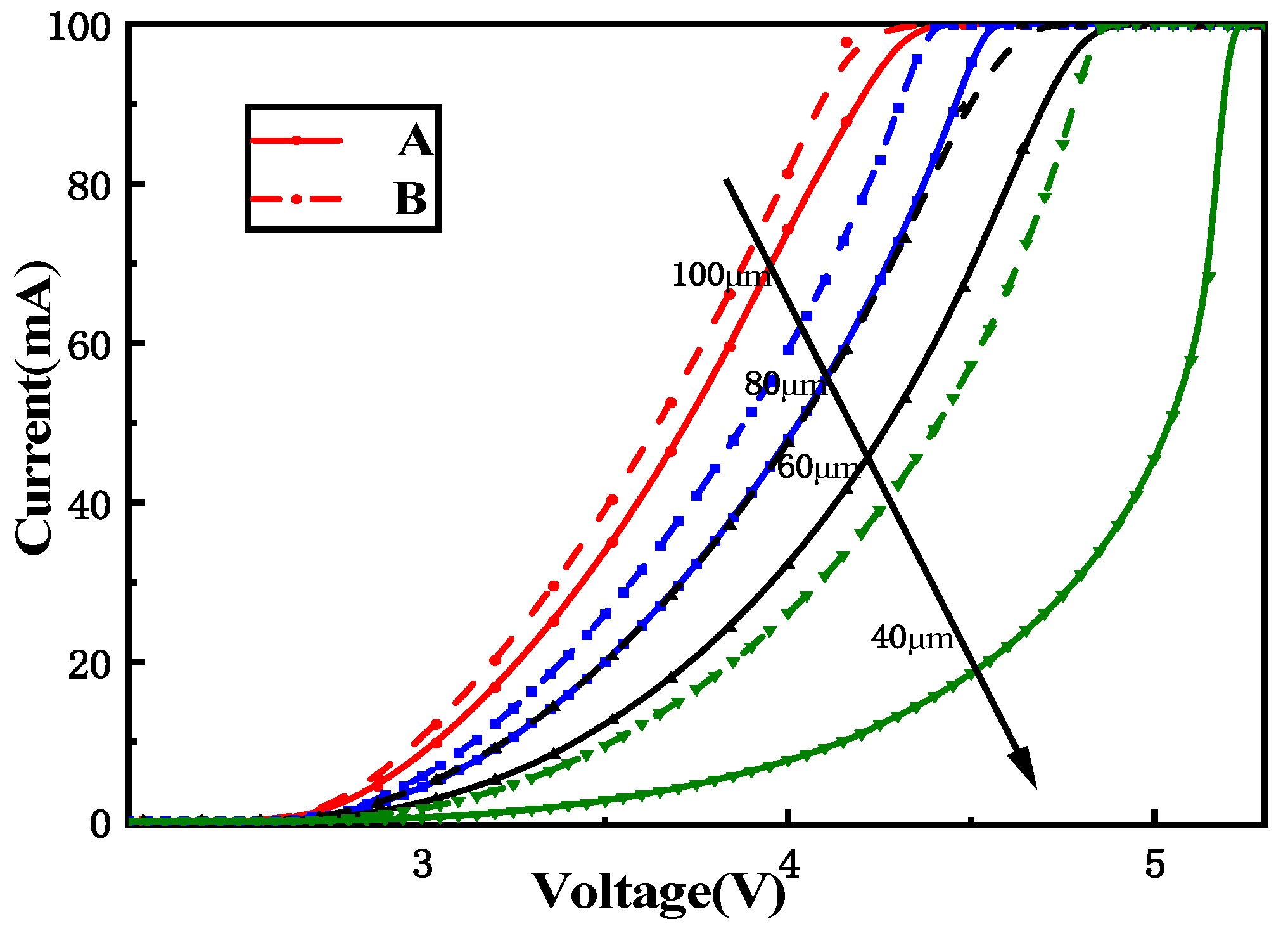
3.1. Influence of Different ITO Sizes on Optoelectronic Properties

Structure A and B represent Micro LEDs whose ITO size is smaller than and equal to the area of the light-emitting area, respectively. Figure 2 shows the I-V characteristic curves of the two structures under different light-emitting area sizes; it can be seen that at the same light-emitting area size, the series resistance of A is smaller than that of B, which is because of the increase of ohmic contact area between the P-GaN and ITO, which reduces the voltage of the device. As the size of the light-emitting area of the Micro LED decreases, the series resistance increases; as the contact area between the P-GaN and the ITO decreases with the decrease, this results in an increase in the contact resistance.
Figure 3 shows the variation curves of the WPE of the two structures with the current density under different light-emitting sizes. Because under the dual action of Auger recombination and carrier leakage, the rise in luminous power will be limited, while the current and voltage can be kept in a high range, so the WPE shows a downward trend. The WPE of B is higher than that of A, because the larger ITO area of B not only means larger light-emitting area and more photons emitted compared with the conventional structure A, but also means larger ohmic contact area and lower voltage. In addition, under the same light-emitting size, the larger the ITO is, the smaller the series resistance is (Figure 2). According to Formula (3), the value of voltage-temperature coefficient S decreases with the decrease of series resistance, so the thermal stability of B is better, which makes the current spreading and the optoelectronic performance of structure B better.
S = d V F d T = n k q ln I F I S + d R s d T I F
where, I S is the reverse saturation current, q is the electronic quantity, k is the Boltzmann constant, T is the absolute temperature and n is the ideal factor. I S is a function of temperature. Under the condition that all impurities in the semiconductor material are ionized and the intrinsic excitation can be ignored, I S can be summarized as:
I S = A e D n τ n n i 2 N A + D P τ P n i 2 N D = C T 3 exp e V g 0 K T
A is the knot area, C is a constant related to junction area and impurity concentration and V g 0 is the potential difference between the conduction band bottom and the valence band top of the PN junction material at absolute zero. Substituting Formula (2) into Formula (1), S can be summarized as:
S = d V F d T = n k q ln C I F + 3 n k q lnT + 3 n k q + 1.5 k T + E a 2 k T 2 I F R s
Figure 3 also shows the variation of the novel structure (B) compared with the conventional structure (A) under four kinds of size. It can be seen that as the chip size decreases, the ITO area has a greater impact on the optoelectronic performance of the Micro LED. Where the size of the light-emitting area is 40 μm and 100 μm, the WPE of the novel structure improves by up to 110% and 18% as shown in Figure 3a and Figure 3d, respectively. A mathematical model can be used to describe this phenomenon. If the size of the light-emitting area is “L” and the distance between the ITO boundary and the boundary of the light-emitting area is “a” (approximately equal to 2 μm), then the area ratio of the ITO to the light-emitting area is “(L − a)2/L2”. Thus, the larger the size “L”, the closer the ratio to “1”, and the smaller the effect of the shrinkage of ITO on the current spreading is. Therefore, the performance of small size Micro LED can be significantly improved on account of the growth of the ITO area.

3.2. Influence of Different Mesa Shapes on Optoelectronic Properties

In this paper, C and D represent the square mesa Micro LED and circular mesa Micro LED in this comparative experiment, respectively. The specific dimensions of Micro LED with two structures are shown in Table 1.
Figure 4 shows the variation curves of WPE and luminous power of Micro LEDs with different mesa shapes under different current densities. As a whole, the WPE is almost the same for C and D; the luminous power of C is a little bit higher than that of D at high current density. However, with the increase in device size and current density, the square Micro LED has better optoelectronic performance. The WPE of the square mesa Micro LED is larger than that of the circular one, because the side surface area of the square light-emitting area is about 13% larger than that of the circular one, which leads to more light-emitting from the sidewall of C, thereby increasing the luminous power. As the current density increases further, more light emits from the sidewall, and the optoelectronic performance gap between the two structures will be widened, and as the size of the light-emitting area increases, the Micro LED with a square mesa will have better stability than the Micro LED with a circular mesa.
To further explore the performance differences of Micro LEDs with different mesa shapes in different sizes, the thermal characteristics of devices with two structures were tested under the current of 20 mA. Figure 5 shows the thermal resistance of Micro LEDs with square and circular mesa of different sizes. The thermal resistance of the square mesa Micro LED is slightly higher than that of the circular one when the size is small, which is the reason why the WPE of the D-I is slightly higher than that of C-I. With the increase in chip size, the thermal resistance of the two structures achieves the same level, that is, the thermal characteristics of the two structures are not the main factor affecting WPE in the case of large mesa size; the difference of luminous power caused by the light-emitting from the sidewall is the main reason for the difference in the optoelectronic performance of devices with two kinds of structures. Therefore, in Micro LEDs of small size, thermal factors are the cause why the square mesa cannot achieve a better optoelectronic performance than the circular one. However, with the increase in chip size, the Micro LED of the square mesa has a better optoelectronic performance due to the better luminous power.

4. Conclusions

In this paper, Micro LEDs with a light-emitting area size of 40–100 μm and an ITO size smaller than or equal to the light-emitting area size were designed and fabricated respectively. After testing and analyzing these Micro LEDs with different structures, it is found that when the area of ITO is equal to the area of the light-emitting area, the optoelectronic performance of the Micro LED is obviously better than that of conventional Micro LEDs with the area of ITO smaller than the area of the light-emitting area. When the area of the light-emitting area is 40 μm, the improvement of WPE by the new structure exceeds 50%, and with the increase in the current density, there is still a trend to improve WPE. According to this experimental result, we can improve the overall performance of the device by increasing the contact area between ITO and P-GaN, especially in small size Micro LEDs. Furthermore, Micro LEDs with square and circular mesa of different sizes were designed and fabricated, which has the structure that the area of ITO is equal to the area of the light-emitting area. It is found that the WPE of the Micro LED with a square mesa is slightly higher than that of the Micro LED with a circular mesa at a high current density on account that the light emits from sidewall, which is instructive for us to choose the mesa shape of Micro LED as Micro LED usually works under high current density. And as the size of the light-emitting area increases, the Micro LED with a square mesa will have better stability than the Micro LED with a circular mesa. In the future display array fabrication, we can extract the light from the sidewall of Micro LED on the square mesa to the pixel position, which will be of great help to the future research of Micro LED display array. In general, the square mesa Micro LED with the ITO size equal to the area of the light emitting area exhibits better optoelectronic properties, which provides a new idea for further reducing the size of the Micro LED and improving the performance of the Micro LEDs in the future.

Author Contributions

Conceptualization, W.G. and A.F.; methodology, A.F.; formal analysis, A.F. and H.X.; investigation, A.F., J.C. and M.L.; writing—original draft preparation, A.F. and H.X.; writing—review and editing, A.F., H.X. and J.L.; supervision, W.G. All authors have read and agreed to the published version of the manuscript.

Funding

This research was funded by National key R&D program of China (No. 2017YFB0402803).

Institutional Review Board Statement

Not applicable.

Informed Consent Statement

Not applicable.

Data Availability Statement

Not applicable.

Conflicts of Interest

The authors declare no conflict of interest. The funders had no role in the design of the study; in the collection, analyses, or interpretation of data; in the writing of the manuscript; or in the decision to publish the results.

References

  1. Zhou, F.; Xu, W.; Ren, F.; Zhou, D.; Chen, D.; Zhang, R.; Zheng, Y.; Zhu, T.; Lu, H. High-Voltage Quasi-Vertical GaN Junction Barrier Schottky Diode with Fast Switching Characteristics. IEEE Electron Device Lett. 2021, 42, 974–977. [Google Scholar] [CrossRef]
  2. Hwangbo, S.; Hu, L.; Hoang, A.T.; Choi, J.Y.; Ahn, J.H. Wafer-scale monolithic integration of full-colour micro-LED display using MoS2 transistor. Nat. Nanotechnol. 2022, 17, 500–506. [Google Scholar] [CrossRef] [PubMed]
  3. Du, Z.; Li, D.; Guo, W.; Xiong, F.; Tang, P.; Zhou, X.; Zhang, Y.; Guo, T.; Yan, Q.; Sun, J. Quantum Dot Color Conversion Efficiency Enhancement in Micro-Light-Emitting Diodes by Non-radiative Energy Transfer. IEEE Electron Device Lett. 2021, 42, 1184–1187. [Google Scholar] [CrossRef]
  4. Huang, C.; Cheng, Y.; Tsao, Y.; Liu, X.; Kuo, H. Micro-LED backlight module by deep reinforcement learning and micro-macro-hybrid environment control agent. Photon. Res. 2022, 10, 269–279. [Google Scholar] [CrossRef]
  5. Shan, X.; Zhu, S.; Qiu, P.; Qian, Z.; Lin, R.; Wang, Z.; Cui, X.; Liu, R. Multifunctional Ultraviolet-C Micro-LED With Monolithically Integrated Photodetector for Optical Wireless Communication. J. Lightwave Technol. 2022, 40, 490–498. [Google Scholar] [CrossRef]
  6. Kim, T.; Yoon, Y.; Oh, S.; Cha, Y.; Hong, I.; Cho, M.; Hong, C.; Choi, H.; Kwak, J. Opposite Behavior of Multilayer Graphene/Indium-Tin-Oxide p-Electrode for Gallium Nitride Based-Light Emitting Diodes Depending on Thickness of Indium-Tin-Oxide Layer. J. Nanosci. Nanotechnol. 2018, 18, 6106–6111. [Google Scholar] [CrossRef] [PubMed]
  7. Min, J.; Kwak, H.; Kim, K.; Jeong, W.; Lee, D. Very thin ITO/metal mesh hybrid films for a high-performance transparent conductive layer in GaN-based light-emitting diodes. Nanotechnology. 2017, 28, 045201. [Google Scholar] [CrossRef] [PubMed]
  8. Lu, W.; Aplin, D.; Clawson, A.R.; Yu, P. Effects of the gas ambient in thermal activation of Mg-doped p-GaN on Hall effect and photoluminescence. J. Vac. Sci. Technol. A 2013, 31, 011502. [Google Scholar] [CrossRef]
  9. Cheng, L.; Wu, Y. InGaN-GaN Light Emitting Diode Performance Improved by Roughening Indium Tin Oxide Window Layer via Natural Lithography. Electrochem. Solid-State Lett. 2010, 13, J8–J10. [Google Scholar] [CrossRef]
  10. Xu, J.; Zhang, W.; Peng, M.; Dai, J.; Chen, C. Light-extraction enhancement of GaN-based 395 nm flip-chip light-emitting diodes by an Al-doped ITO transparent conductive electrode. Opt. Lett. 2018, 43, 2684–2687. [Google Scholar] [CrossRef] [PubMed]
  11. Yang, F.; Xu, Y.; Li, L.; Cai, X.; Li, J.; Tao, J.; Zheng, S.; Cao, B.; Xu, K. Optical and microstructural characterization of Micro-LED with sidewall treatment. J. Phys. D-Appl. Phys. 2022, 55, 43. [Google Scholar] [CrossRef]
  12. Chen, P.; Chang, L.C.; Tsai, C.H.; Lee, Y.C.; Lai, W.C.; Wu, M.L.; Kuo, C.H.; Sheu, J.k. GaN-Based Light-Emitting Diodes with Pillar Structures Around the Mesa Region. IEEE J. Quantum Electron. 2010, 46, 1066–1071. [Google Scholar] [CrossRef]
  13. Boussadi, Y.; Rochat, N.; Barnes, J.P.; Bakir, B.; Ferrands, P.; Masenelli, B.; Licitra, C. Investigation of sidewall damage induced by reactive ion etching on AlGaInP MESA for micro-LED application. J. Lumines. 2021, 234, 117937. [Google Scholar] [CrossRef]
  14. Wang, P.; Gan, Z.; Liu, S. Improved light extraction of GaN-based light-emitting diodes with surface-patterned ITO. Opt. Laser Technol. 2009, 41, 823–826. [Google Scholar] [CrossRef]
  15. Lee, Y.; Reddy, M.; Kim, B.; Park, C. Surface morphological, structural, electrical and optical properties of GaN-based light-emitting diodes using submicron-scaled Ag islands and ITO thin films. Opt. Mater. 2018, 81, 109–114. [Google Scholar] [CrossRef]
  16. Park, J.; Kim, J.; Kim, J.; Kim, D.; Na, J.; Kim, S. Formation of an indium tin oxide nanodot/Ag nanowire electrode as a current spreader for near ultraviolet AlGaN-based light-emitting diodes. Nanotechnology 2017, 28, 045205. [Google Scholar] [CrossRef] [PubMed]
Figure 1. Micro LED (a) with ITO smaller than light emitting area (b) with ITO equal to light emitting area (c) with circular mesa (ITO equal to light emitting area).
Crystals 12 01593 g001
Figure 2. I–V curves of Micro LEDs with ITO size smaller than (A) and equal to (B) the light-emitting area size.
Crystals 12 01593 g002
Figure 3. WPE vs. current densities of Micro LED A and B (a) 40 μm (b) 60 μm (c) 80 μm (d) 100 μm.
Crystals 12 01593 g003
Figure 4. WPE and luminous power of C and D at different current densities, (a)–(d) correspond to experimental group I–IV (The size of the mesa increases gradually).
Crystals 12 01593 g004
Figure 5. Thermal resistance of C and D with different mesa sizes at 20 mA current.
Crystals 12 01593 g005
Table 1. Specific dimensions of C and D.
GroupLength of C (L)Area of CDiameter of D (R)Area of D
I30 μm900 μm234 μm908 μm2
II40 μm1600 μm245 μm1590 μm2
III80 μm6400 μm290 μm6362 μm2
IV100 μm10,000 μm2113 μm10,028 μm2
Publisher’s Note: MDPI stays neutral with regard to jurisdictional claims in published maps and institutional affiliations.

