1. Introduction
With the development of science and technology, light-emitting diodes (LEDs) play an increasingly important role in our daily life. Since the birth of gallium nitride (GaN)-based LEDs, they have greatly promoted the development of lighting and display fields. However, there are still problems in the development, such as the difficulty of heavy doping of p-type GaN. This means that the conductivity of p-type GaN is relatively poor, so that the current is difficult to spread to achieve sufficient current injection. For this reason, transparent electrodes came into being. Indium tin oxide (ITO) is the most representative transparent electrode material, which has excellent electrical conductivity and high transparency in the visible band [
1,
2,
3,
4]. Nevertheless, from the perspective of sustainable development, ITO is inferior to graphene because of the scarcity of indium [
5,
6]. In addition, graphene performs better than ITO on flexible substrates. These factors make graphene one of the most viable potential transparent electrode materials [
7].
In the growth of graphene, metals play a crucial catalytic role. The catalytic mechanism is mainly divided into two types [
8]: one is the carbon segregation and precipitation mechanism represented by nickel, under which more layers of graphene are grown; the other is the surface adsorption mechanism represented by copper, under which the number of graphene layers grown is lesser. Both of these mechanisms are widely used in the growth of graphene.
However, the vital role played by metal catalysts in graphene growth means that the growth of high-quality graphene is often inseparable from metals. As a result, as-grown graphene is always attached to the surface of metal substrates [
9,
10,
11], which is difficult to use in electronic devices directly. There are some solutions to this problem: for example, graphene can be transferred from the metal substrates to the target substrates, but in this process greater or lesser contamination and defects will inevitably be introduced. In addition, graphene can be directly grown on the target substrates, but without metal catalysis the growth of graphene is often more difficult [
12,
13].
To solve this problem, in this paper we propose a nickel-assisted transfer-free technology of CVD graphene on GaN. In this method, nickel film is used to catalyze the growth of high-quality graphene, and it is removed by the penetration etching process to realize the contact of graphene with the target substrates, so as to avoid the transfer process. In addition, nickel is not only used as a catalyst, but also as a mask to etch the LED mesas. The measurement results show that the as-grown graphene film effectively improves the electrical performance of LEDs. The effects of different growth time on the performance of LEDs are compared as well. The process is simple, efficient and highly repeatable, which directly realizes good, tight contact between graphene and GaN, providing a solution for the integration of graphene and GaN devices.
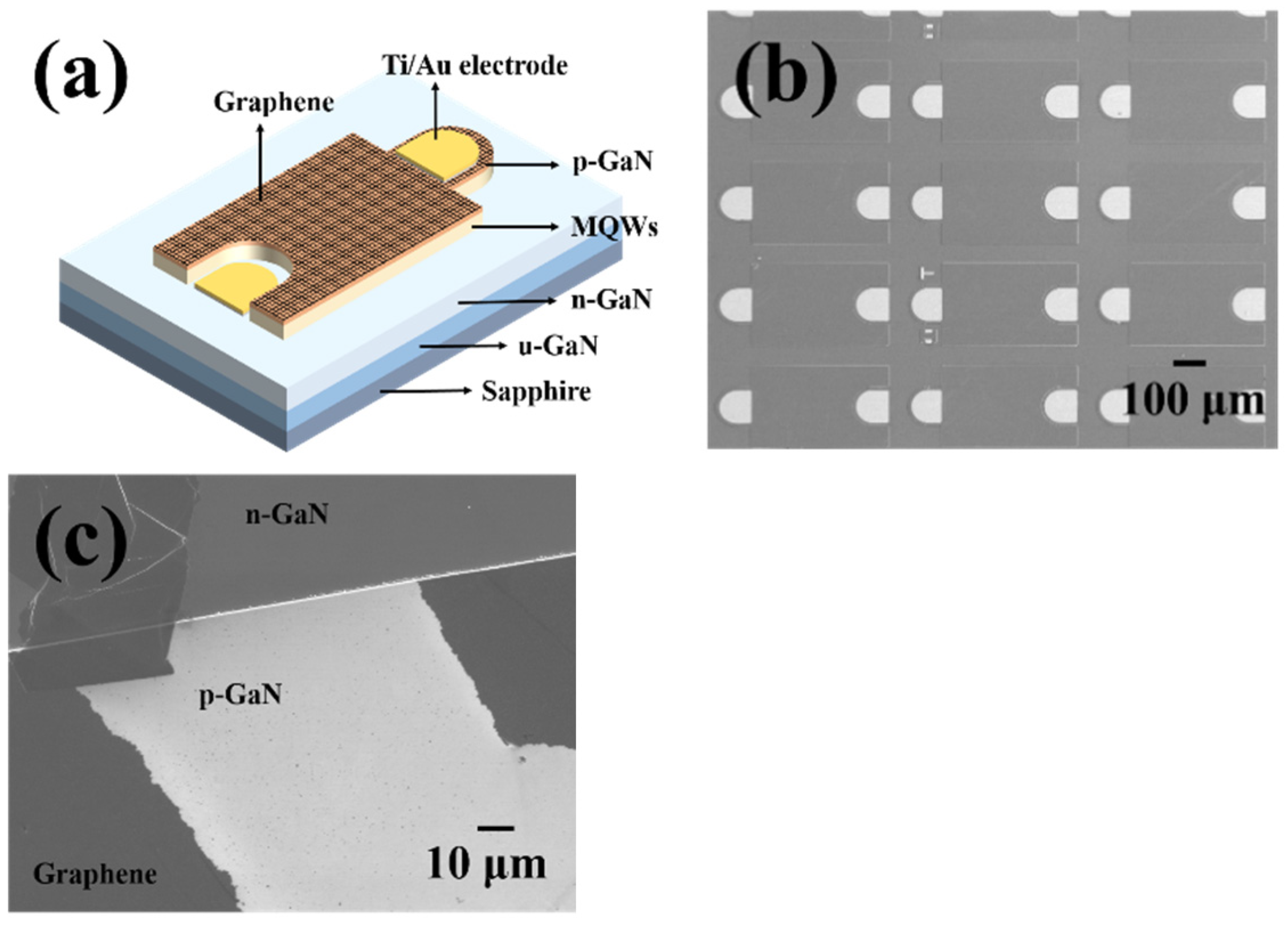
2. Materials and Methods
Since lift-off photolithography of metal electrodes after graphene growth may cause some damage to graphene, in order to pursue more stable and excellent electrical performance nickel is selected as the catalyst to grow graphene with more layers, reducing the impact of subsequent processes on the continuity of graphene.
Figure 1 shows a schematic diagram of the process flow of the LEDs in this paper. The epitaxial wafers used were provided by Xiangneng Hualei Optoelectronics Company. First, a 300 nm nickel film was photolithographically sputtered on the epitaxial wafer as the subsequent etching mask and growth catalyst. The 260 × 515 μm
2 LED mesas were etched with inductively coupled plasma (ICP) at an etching ratio of approximately 1:80 for nickel and GaN, as shown in
Figure 1b. The samples were subsequently grown in cold-wall plasma-enhanced chemical vapor deposition (PECVD) at 600 °C and 6 mbar, under an atmosphere of CH
4/H
2/Ar (5/20/960 sccm) and at a plasma power of 40 W. As shown in
Figure 1d, after the growth of graphene, PMMA (poly(methyl-methacrylate)) was spin-coated on the sample (3000 rpm for 30 s) and baked at 150 °C for 10 min. It is approximately 150 nm thick. Then the sample was put into the etching solution for more than four hours (CuSO
4:HCl:H
2O = 10 g:50 mL:50 mL). The etching solution can pass through the PMMA and graphene to slowly etch Ni film. Since PMMA is in close contact with graphene and n-GaN, after the metal is etched, PMMA and graphene will fall onto the surface of the sample instead of floating away in the solution. Then PMMA was removed by acetone and isopropyl alcohol (
Figure 1f). Due to the weak van der Waals force on the surface of graphene, it is necessary to remove the graphene on the electrode area with oxygen plasma etching to prevent metal electrodes from falling off, as shown in
Figure 1g. Finally, 15 nm Ti and 300 nm Au were sputtered as electrodes and annealed in a 450 °C vacuum for five minutes (
Figure 1h).
Figure 2a shows the structure of the LEDs.
Figure 2b shows the scanning electron microscope (SEM) image of the LED arrays (SE2 mode). An area of intentionally broken graphene has a higher contrast for better observation of graphene film, which is characterized by SEM (in-lens mode), as shown in
Figure 2c. Since the in-lens mode has higher resolution, which is more suitable for observing the microscopic morphology, the graphene layer can be clearly seen in
Figure 2c. The white boundary line in the image is the edge of the LED mesa, below which is the p-GaN and graphene on the mesa, and above which is the n-GaN beside the mesa. The dark film is graphene, and p-GaN is exposed in the broken area of graphene, corresponding to the white area in the image. It can be clearly seen that the graphene film has been broken and folded in this area, and even some graphene falls on n-GaN.
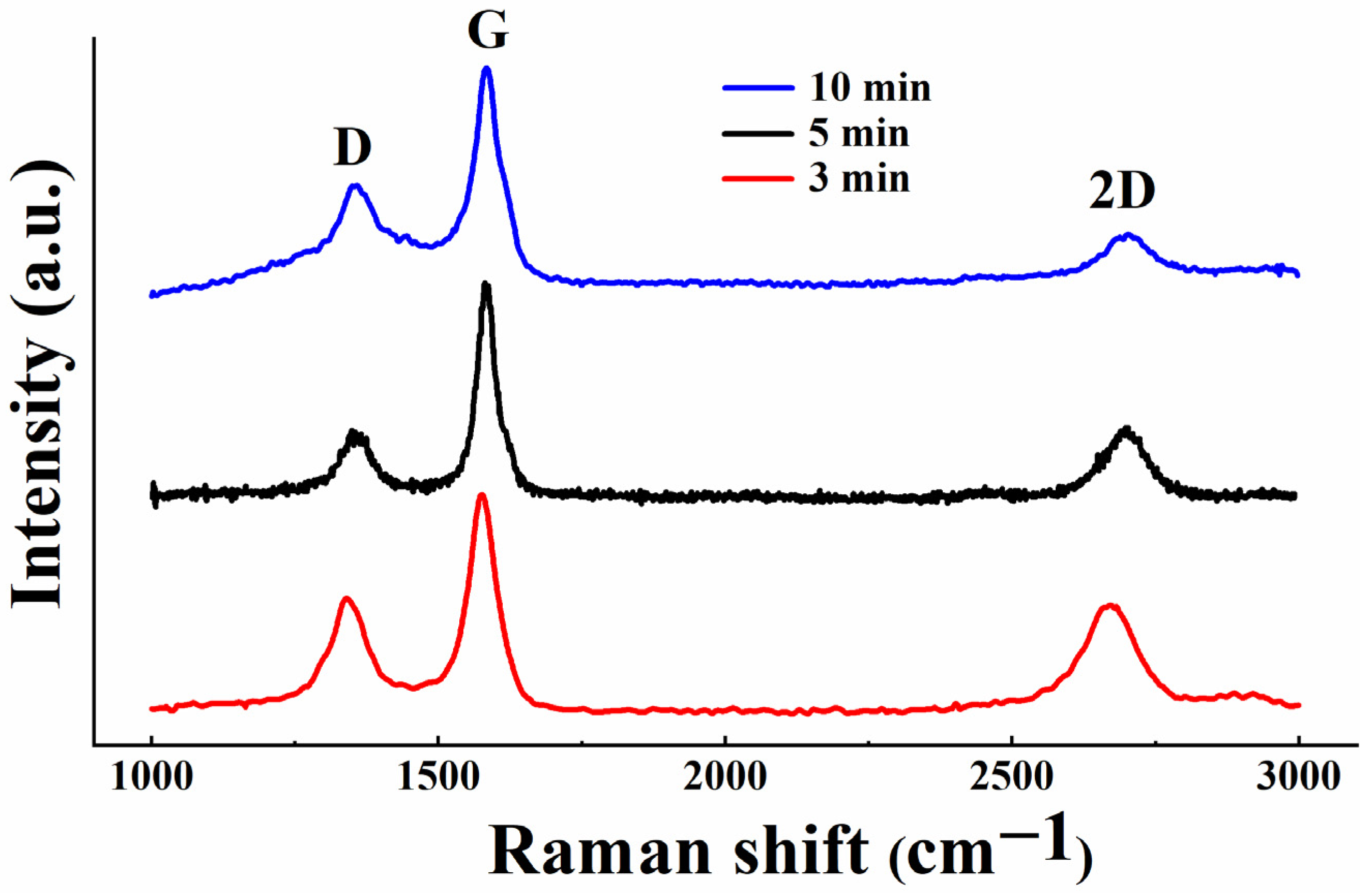
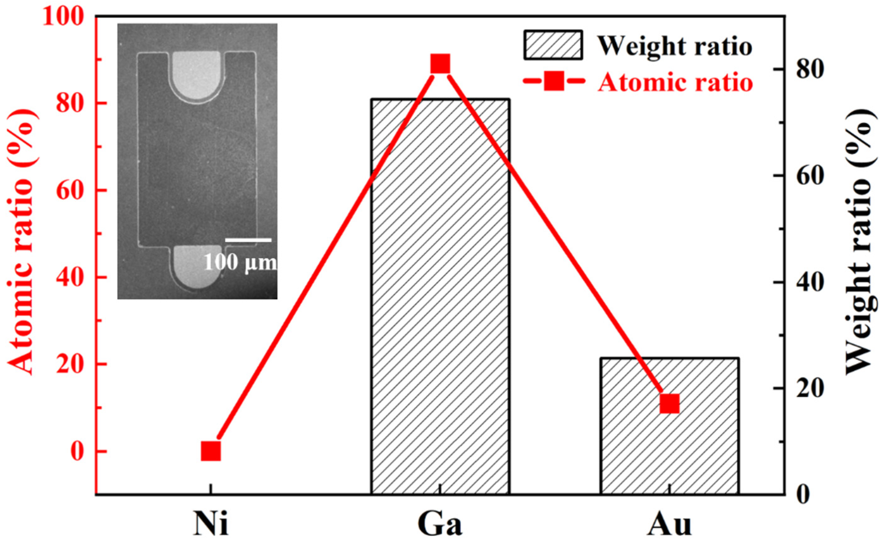
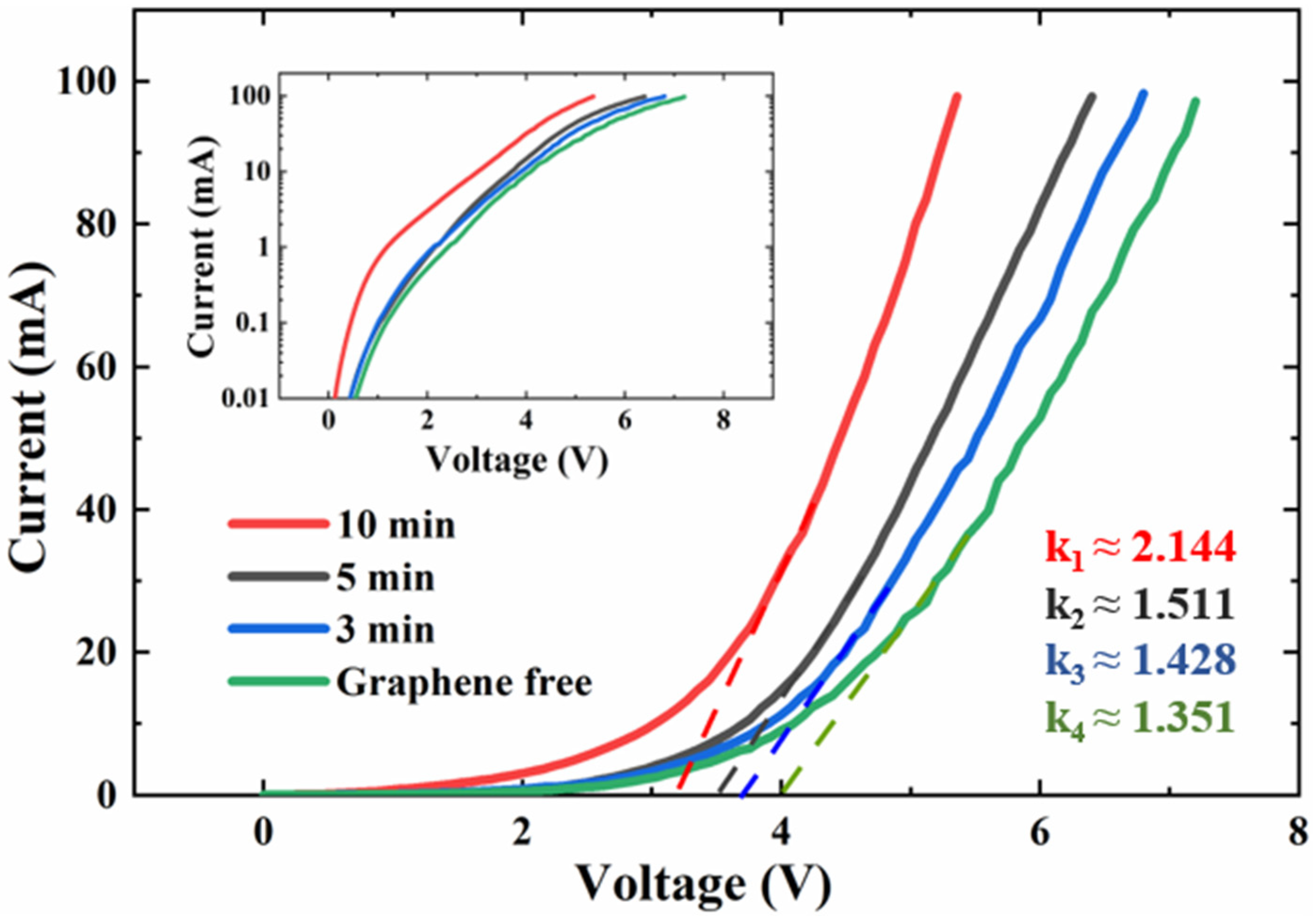
3. Results and Discussion
In order to study the effect of graphene of different qualities on LED performance, LEDs with different graphene growth time were fabricated.
Figure 3 shows the Raman characterization of graphene with different growth time after the fabrication of LEDs. The number of graphene layers is usually estimated in terms of the 2D/G ratio and the shape of the peaks [
14]. It can be seen that with the increase of growth time, the 2D/G ratio gradually decreases, indicating that the number of graphene layers gradually increases. The graphene is estimated to be about 5–10 layers thick, based on both the Raman spectra [
15] and our previous atomic force microscopy (AFM) measurement [
12]. In addition, the Raman characterization was performed after the LEDs were fabricated, indicating that the graphene still maintains good quality after the lift-off photolithography of the metal electrodes.
Figure 4 is the energy dispersive spectroscopy (EDS) surface scanning result, inset is the characterized area and the characterized elements are Ni, Ga and Au. Among them, the molecular ratio of Ni is 0.01%, and the weight ratio is 0.02%. This indicates that the Ni film has been substantially etched away.
In addition to the fabrication of LEDs with graphene, graphene-free LEDs were also fabricated for comparison using basically the same process, and their current–voltage characteristics are shown in
Figure 5. The inset is the current–voltage characteristics in semi-log scale. The dotted auxiliary lines are the reverse extension lines of the nearly linear part of the current–voltage characteristic curves, and their intersections with the abscissa represent the turn-on voltages of LEDs. The turn-on voltages of LEDs with growth time of 10 min, 5 min, 3 min and without graphene are about 3.2 V, 3.5 V, 3.7 V and 4 V, respectively; the operating voltages at 20 mA are about 3.5 V, 4.2 V, 4.4 V and 4.7 V, respectively. The slopes (k
1–k
4) of these auxiliary lines, which are mainly related to the LED series resistance, are also shown in
Figure 5. Compared with graphene-free LEDs, the current spreading effect of graphene will reduce the series resistance of graphene-coated LEDs. Therefore, with the increase of growth time, the slope increases and the series resistance decreases. It can be inferred that graphene improves electrical performance of LEDs, and the thicker the graphene the greater the improvement, which may be attributed to its better continuity. From the inset, it is clear that these LEDs have a certain degree of leakage current before reaching their respective turn-on voltage, which may be related to the recombination current in the barrier area. Compared with graphene-free LEDs, the leakage current of LEDs with a growth time of 3 min and 5 min is not much different. However, the LEDs with graphene grown for 10 min have serious leakage current. This may be due to the fact that many carbon atoms are adsorbed on the sidewalls of the mesas because the growth time is too long, even though graphene is not formed because there is no metal catalyst on the sidewalls. Therefore, properly increasing the growth time can effectively improve the electrical performance of LEDs.
Figure 6 is the optical microscope luminescence images of LEDs with and without graphene at 20 mA. Even though thicker graphene theoretically blocks more light [
10], the difference in luminescence of LEDs coated with different graphene is still small when observed under an optical microscope, so only a representative graphene-coated LED is shown. It can be seen that the graphene-free LED only emits light near the metal electrodes, while the graphene-coated LED emits light evenly on the entire mesa. This shows that graphene plays a good role in current expansion, which indicates that graphene plays a good role in current spreading.
4. Conclusions
In this paper, a method of growing transfer-free graphene on GaN by PECVD is introduced. LEDs with different thickness of graphene are fabricated by controlling the growth time. In the whole process, the Ni film is not only used as the mask for mesa etching but also as the catalyst for graphene growth, which is subsequently removed to achieve direct contact between graphene and GaN. When the growth time is less than ten minutes, the thickness of graphene increases with the growth time. The measurement results show that graphene realizes current spreading and effectively improves the electrical performance of LEDs, although excessive growth time may lead to current leakage of LEDs. This method makes CVD graphene achieve good contact with GaN substrate, avoiding the defects and impurities introduced in the transfer process.
Author Contributions
Conceptualization, P.T. and J.S.; methodology, P.T., F.X. and J.S.; investigation, K.L.; data curation, P.T. and Y.M.; writing—original draft preparation, P.T.; writing—review and editing, P.T., Z.D. and J.S.; supervision, W.G. and J.S. All authors have read and agreed to the published version of the manuscript.
Funding
This research was funded by the Fujian Provincial Projects (2021HZ0114, 2021J01583, 2021L3004), the Fujian Science & Technology Innovation Laboratory for Optoelectronic Information of China (2021ZZ122, 2020ZZ110), the National Key R&D Program of China (2018YFA0209004) and the Beijing Municipal Commission of Education (KM201810005029).
Data Availability Statement
Not applicable.
Conflicts of Interest
The authors declare no conflict of interest.
References
- Amano, H.; Kito, M.; Hiramatsu, K.; Akasaki, I. P-type conduction in Mg-doped GaN treated with low-energy electron-beam irradiation (LEEBI). Jpn. J. Appl. Phys. 1989, 28, 2112–2114. [Google Scholar] [CrossRef] [Green Version]
- Nakamura, S.; Mukai, T.; Senoh, M.; Lwasa, N. Thermal annealing effects on p-type Mg-doped GaN films. Jpn. J. Appl. Phys. 1992, 31, 139–142. [Google Scholar] [CrossRef]
- Neugebauer, J.; Vandewalle, C.G. Role of hydrogen in doping of GaN. Appl. Phys. Lett. 1996, 68, 1829–1831. [Google Scholar] [CrossRef] [Green Version]
- Hamberg, I.; Granqvist, C.G. Evaporated Sn-doped In2O3 films: Basic optical properties and applications to energy-efficient windows. J. Appl. Phys. 1986, 60, 123–160. [Google Scholar] [CrossRef]
- Li, F.; Lin, Z.; Zhang, B.; Zhang, Y.; Wu, C.; Guo, T. Fabrication of flexible conductive graphene/Ag/Al-doped zinc oxide multilayer films for application in flexible organic light-emitting diodes. Org. Electron. 2013, 14, 2139–2143. [Google Scholar] [CrossRef]
- Jiang, G.; Tian, H.; Wang, X.-F.; Hirtz, T.; Wu, F.; Qiao, Y.-C.; Gou, G.-Y.; Wei, Y.-H.; Yang, J.-M.; Yang, S.; et al. An efficient flexible graphene-based light-emitting device. Nanoscale Adv. 2019, 1, 4745–4754. [Google Scholar] [CrossRef] [Green Version]
- Bolotin, K.; Sikes, K.; Jiang, Z.; Klima, M.; Fudenberg, G.; Hone, J.; Kim, P.; Stormer, H. Ultrahigh electron mobility in suspended graphene. Solid State Commun. 2008, 146, 351–355. [Google Scholar] [CrossRef] [Green Version]
- Li, X.; Cai, W.; Colombo, L.; Ruoff, R.S. Evolution of graphene growth on Ni and Cu by carbon isotope labeling. Nano Lett. 2009, 9, 4268–4272. [Google Scholar] [CrossRef] [PubMed] [Green Version]
- Sun, J.; Lindvall, N.; Cole, M.T.; Angel, K.T.T.; Wang, T.; Teo, K.B.K.; Chua, D.H.C.; Liu, J.; Yurgens, A. Low partial pressure chemical vapor deposition of graphene on copper. IEEE Trans. Nanotechnol. 2012, 11, 255–260. [Google Scholar] [CrossRef]
- Kim, B.-J.; Lee, C.; Jung, Y.; Baik, K.H.; Mastro, M.A.; Hite, J.K.; Eddy, C.R., Jr.; Kim, J. Large-area transparent conductive few-layer graphene electrode in GaN-based ultra-violet light-emitting diodes. Appl. Phys. Lett. 2011, 99, 143101. [Google Scholar] [CrossRef]
- Sutter, P.; Sadowski, J.T.; Sutter, E. Graphene on Pt (111): Growth and substrate interaction. Phys. Rev. B 2009, 80, 245411. [Google Scholar] [CrossRef] [Green Version]
- Xiong, F.; Sun, J.; Cole, M.T.; Guo, W.; Yan, C.; Dong, Y.; Wang, L.; Du, Z.; Feng, S.; Li, X.; et al. GaN LEDs with in situ synthesized transparent graphene heat-spreading electrodes fabricated by PECVD and penetration etching. J. Mater. Chem. C 2022, 10, 6794–6804. [Google Scholar] [CrossRef]
- Giannazzo, F.; Fisichella, G.; Greco, G.; La Magna, A.; Roccaforte, F.; Pecz, B.; Yakimova, R.; Dagher, R.; Michon, A.; Cordier, Y. Graphene integration with nitride semiconductors for high power and high frequency electronics. Phys. Status Solidi A 2017, 214, 1600460. [Google Scholar] [CrossRef]
- Ferrari, A.C.; Meyer, J.C.; Scardaci, V.; Casiraghi, C.; Lazzeri, M.; Mauri, F.; Piscanec, S.; Jiang, D.; Novoselov, K.S.; Roth, S.; et al. Raman spectrum of graphene and graphene layers. Phys. Rev. Lett. 2006, 97, 187401. [Google Scholar] [CrossRef] [PubMed] [Green Version]
- Bi, H.; Sun, S.; Huang, F.; Xie, X.; Jiang, M. Direct growth of few-layer graphene films on SiO2 substrates and their photovoltaic applications. J. Mater. Chem. 2012, 22, 411–416. [Google Scholar] [CrossRef]
| Publisher’s Note: MDPI stays neutral with regard to jurisdictional claims in published maps and institutional affiliations. |
© 2022 by the authors. Licensee MDPI, Basel, Switzerland. This article is an open access article distributed under the terms and conditions of the Creative Commons Attribution (CC BY) license (https://creativecommons.org/licenses/by/4.0/).