Article

Impact of CdCl2 Treatment in CdTe Thin Film Grown on Ultra-Thin Glass Substrate via Close Spaced Sublimation

by
Nowshad Amin
1,2,*,
Mohammad Rezaul Karim
3,4 and
Zeid Abdullah ALOthman
5,*
1
College of Engineering, Universiti Tenaga Nasional (The Energy University), Jalan IKRAM-UNITEN, Kajang 43000, Malaysia
2
Institute of Sustainable Energy, Universiti Tenaga Nasional (The Energy University), Jalan IKRAM-UNITEN, Kajang 43000, Malaysia
3
Center of Excellence for Research in Engineering Materials (CEREM), Deanship of Scientific Research (DSR), College of Engineering, King Saud University, P.O. Box 800, Riyadh 11421, Saudi Arabia
4
K.A.CARE Energy Research and Innovation Center, Riyadh 11451, Saudi Arabia
5
Chemistry Department, College of Science, King Saud University, P.O. Box 2455, Riyadh 11451, Saudi Arabia
*
Authors to whom correspondence should be addressed.
Crystals 2021, 11(4), 390; https://doi.org/10.3390/cryst11040390
Submission received: 22 February 2021 / Revised: 24 March 2021 / Accepted: 29 March 2021 / Published: 7 April 2021
(This article belongs to the Special Issue Synthesis, Structure and Property Analysis of Crystalline Layers)

Abstract

:
In this study, close-spaced sublimation (CSS) grown cadmium telluride (CdTe) thin films with good adhesion to 100 µm thin Schott D263T ultra-thin glass (UTG) were investigated. Cadmium chloride (CdCl2) treatment in vacuum ambient was executed to enhance the film quality and optoelectrical properties of CdTe thin film. The post-deposition annealing temperature ranging from 360–420 °C was examined to improve the CdTe film quality on UTG substrate. Various characterization techniques have been used to observe the compositional, morphological, optical, as well as electrical properties. Scanning electron microscopy (SEM) verified that the CdTe morphology and grain size could be controlled via CdCl2 treatment temperature. Energy Dispersive X-Ray Analysis (EDX) results confirmed that the annealing temperature range of 375–390 °C yielded the stoichiometric CdTe films. UV-Vis analysis estimated the post-treatment bandgap energy in the range of 1.39–1.46 eV. Carrier concentration and resistivity were obtained in the order of 1013 cm−3 and 104 Ω-cm, respectively. All the experimental results established that the CdCl2 treatment temperature range of 390–405 °C might be considered as the optimum process temperature for the deposition of CdTe solar cell on UTG substrate in close-spaced sublimation (CSS) method.

1. Introduction

CdTe thin-film solar cells are a promising choice for terrestrial utilization [1]. CdTe has an optimal direct band gap of 1.5 eV [2]. Available CdTe structures are namely zinc blende (cubic) or wurtzite (hexagonal) form [3]. Having a high absorption coefficient (>104 cm−1) and simplicity of deposition, the light to be converted to electricity in a few micrometer thin CdTe layers which allowed fabrication on various type of substrates i.e., glass, foils, polymers, and ultra-thin glass (UTG) for lightweight and bendable configurations [4]. Soda-lime glass (SLG) is the most popular glass used in thin-film fabrication; however, because of its low thermal stability and transmittance, borosilicate glass has become a choice for superstrate CdTe thin films. Boron makes borosilicate glass less reactive with additives, and this glass type is about ten times less prone to corrosion than SLG [5]. Portability and adaptability introduce lower fabrication cost, matchable structures, and thermally stable growth up to the desired CdTe temperature (~700 °C) using borosilicate UTG substrates [6]. In addition, ITO coating by distributing a thin but uniform layer of indium tin oxide over a glass substrate as the transparent conductive oxide (TCO), is applicable for different types of glass to reduce the resistance of the glass. Hence, in this study, ITO-coated 100-micron thin borosilicate glass substrate as presented in Figure 1 is utilized considering the proposed high-temperature deposition using CSS and annealing. A thin film of CdS often completes the n-type side of the device and interfaces with the CdTe. The best efficiency obtained with laboratory-scale cells using this technology is 22.1%, achieved by First Solar. The manufacture of the CdS/CdTe solar cell includes at least four different processes specifically, including a high-temperature process of cadmium telluride preparation, meaning that the control of the quality of each layer and the characteristics of the interface is critical. Besides, recent research has shifted to replacing the traditional CdS window layer. MgxZn1−xO (MZO) is a promising alternative window layer material that has a higher bandgap and has contributed to >18% laboratory cell efficiencies [7,8]. Cadmium selenide (CdSe) is another option. It has been used to adjust bulk lifetime and manipulate absorber bandgap grading to improve photocurrent. Nevertheless. novel approaches related to alternative widow material for CdTe-based devices are still in the primary stage and there is limited knowledge on how these novel window materials affect nucleation, grain size, and recombination [9]. On the other hand, the passivation treatment is a critical factor in processing CdTe thin film with high efficiency [10]. Therefore, to study the treatment effect on the CdTe thin film using UTG substrate by selecting the baseline materials of the standard CdTe thin-film structure, there can be targeted trade-offs and the impact of introducing more uncertainties in results would be avoided. Among various post-deposition treatments, CdCl2 has proven to be the key to elevate the efficiency and stability of CdTe solar cells [11]. The treatment can be conducted through different methods, classified into two types: one-step methods such as vapor transfer and closed space sublimation (CSS) and two-step processes that include evaporation or wet treatment accompanied by annealing. Wet chemical treatment has the advantage of being a non-vacuum procedure that is simple and inexpensive to conduct. In the literature, various approaches for wet treatment have been documented, namely dipping the substrate in the solution or dropping the solution on the substrate surface and annealing step can be performed at different temperatures for different periods and in various atmospheres (air, vacuum, pure O2, etc.). After the residual removal stage and before the back contact formation, devices can be smoothly etched in a bromine/methanol solution to remove the oxidization if full cell fabrication is targeted [12,13].
In general, CdCl2 improves the short circuit current and open circuit voltage through enhancing the crystallite grain nucleation in CdTe, recrystallization, surface amendment, grain boundaries passivation, doping concentration modification, assisting inter-diffusion at the interface, defect density amending, and boosting lifetime of charge carriers in CdTe layer [14]. Through passivation and defect compensation at grain boundaries resulting from post-treatment, treated polycrystalline designs offer better functionality compared to single-crystal cell designs [15]. An impressive increase in efficiency from 1% to higher than 10% has been reported after the CdCl2 treatment process [16]. The CdCl2 reaction might not always induce recrystallization of the CdTe films, considering the initial stress state within the film and the type and conditions of the treatment process. However, even in the treatment cases where there is no recrystallization, this treatment is important due to a reduction in the density of deep levels within the band energy and defect structure modification, boosting overall properties in devices [17].
Prior reports by Moutinho et al. stated that the CdCl2 process effectively decreased the inhomogeneous stress in CSS deposited film especially while 400 °C annealing temperature was proposed [18]. Li et al. determined that for CdCl2 treatment, chlorine was segregated at the grain boundaries, cooperating to passivate the surface [19]. Treatment in air ambient was found to increase the surface oxidation with a lot of chlorine residues left in CdTe surface causing increased resistivity, and reduced acceptor’s density resulted in a reduction of efficiency [20], In contrast, the annealing process in vacuum ambient enhanced open-circuit voltage (Voc) and Jsc, as well as efficiency [11]. It is demonstrated that the vacuum ambient CdCl2 treatment leads to CdTe absorbers with grain refinement, recrystallization, and grain boundary passivation [21] To further understand the effect of gas during the wet CdCl2 treatment process on nanocrystal CdTe cells, Jain et al. studied the annealing of several “oxygen-deficient” devices. The study was in a nitrogen glovebox with less than 0.01 parts per million and air treated devices where oxygen content was 21% and nitrogen content was 78% using the standard method for device fabrication. The authors’ concluded that both devices exhibit diode characteristics, but the device annealed in air exhibits photovoltaic behavior, whereas the device annealed in an oxygen deficient atmosphere does not show any photo-response [22]. Wang et al. demonstrated that air ambient CdCl2 treatment not only improved the grain size and quality but also incorporated Cl and more O into the film, both of which can significantly improve the heterojunction quality and device performance [23]. Dharmadasa et al. concluded from the recent CdCl2 treatment studies that three main elements to consider in this process are Cd, Cl, and O. Air treated devices followed by vacuum annealing process presented better cell performance as O2 may introduce CdO into CdS and CdTe layers, and completely change the wetting properties, growth behavior, or electrical properties of these layers [24].
Annealing temperature also plays a significant role in the CdCl2 treatment process, as CdCl2 treated films present large grains of several microns in size. Still, if annealing temperature oversteps or does not reach specific qualifications, the grains tend to detach from one another that is apparent from the dark areas at the grain borders, suggesting the creation of voids within grains. This grain separation is in line with previous reports in the literature [9]. The impacts of CdCl2 annealing condition on CdTe cells have been already examined [25]. However, the major inspirations for earlier works have been the microstructure of the CdTe absorber and its correlation with the device efficiency [26]. Even though several experiments have been performed so far, complete perception has not yet been achieved [27]. The coaction of CdCl2 on the CdTe layer was examined in different ways and soaked CdTe films in CdCl2 solution using several methods before heat treatment. The CdCl2 solution was formulated as a solvent with methanol or water with different concentrations [28]. Some researchers have coated solid CdCl2 layers on CdTe surfaces with different techniques including vacuum evaporation [29], and the thickness of the evaporated CdCl2 was mostly comparable to the CdTe layer [30]. Oxygen ambient was also studied to act as a p-type dopant in CdTe leading to type conversion [31], and the temperature range from 350 °C to 450 °C was found to be the best for CdCl2 heat treatment within 10 to 20 min [32]. Moreover, multiple improvements such as (a) re-crystallization and grain growth, (b) the CdS/CdTe interface interacts, (c) lifespan extension, (d) passivation of grain boundaries, and overall improvement in full cell efficiencies have been reported [33].
Schott glass substrate was primarily used on silicon cells and recently D263T borosilicate glass model was integrated as an incredibly thin bendable substrate from the earliest PV studies in Germany [24]. Schott D263T glass has been effectively merged into lightweight X-ray optics for space-borne uses [34], organic light-emitting devices (OLED) [35], and photodetectors [36]. In addition, there are more than ten deposition methods used to produce CdTe thin film to date, but CSS is known as the most suitable technique due to the comfort of use and cost-effectiveness [37]. Hence, it is interesting to fabricate and analyze CdTe thin films grown on UTG by the CSS method. Reports on the characterization of CdTe thin films developed on UTG using the CSS technique and CdCl2 treatment using a variety of temperature intervals are yet to be published. Therefore, the main aim of this study is to investigate the impact of CdCl2 treatment annealing temperature in CdTe thin film grown on UTG substrate via CSS.

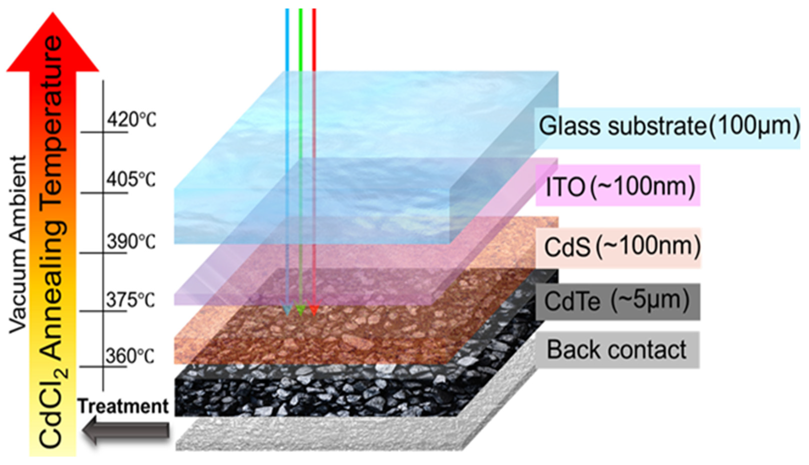
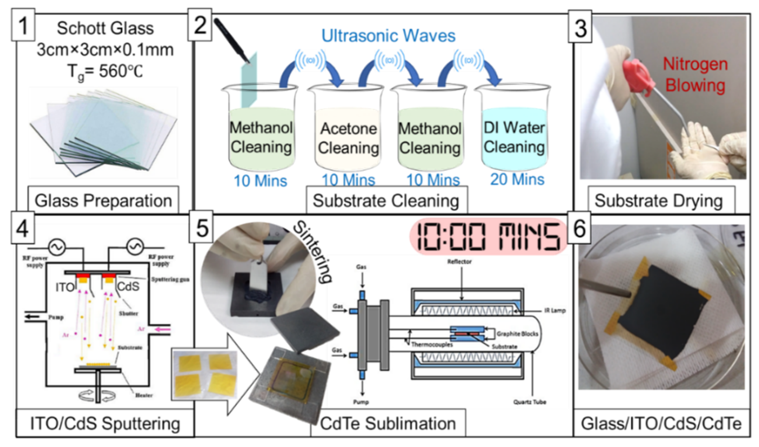
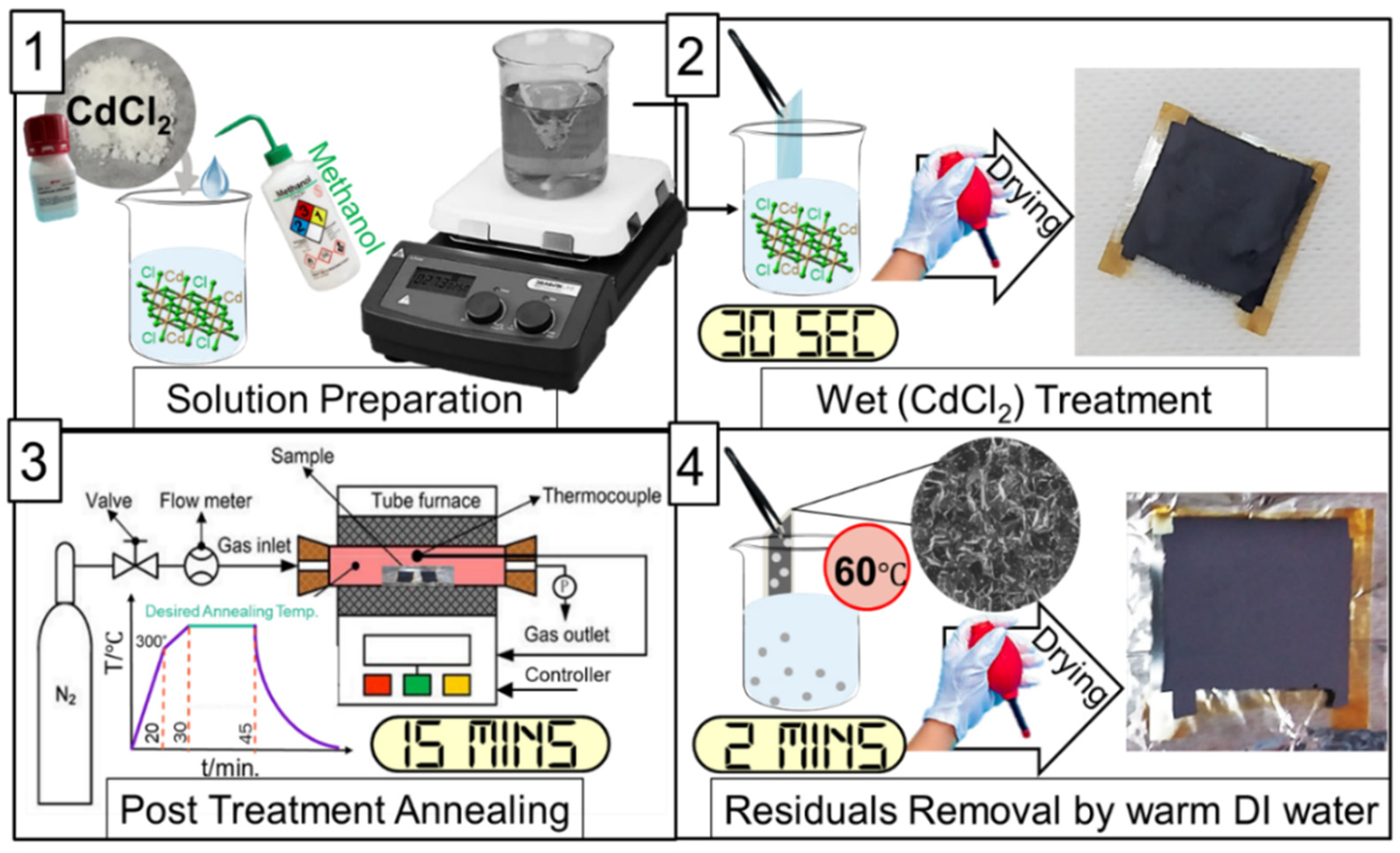
2. Experimental Procedure

2.1. Thin Film Growth

All UTG (3 cm × 3 cm) substrates were cleaned sequentially (Methanol and Acetonefrom Kanto Chemical, Japan, DI water from Younglin AquaMax, Korea) using an ultrasonic bath from Fisher Scientific, UK. Industrial N2 gas was used to dry up the samples after cleaning. Initially, indium doped tin oxide (ITO) and cadmium sulfide (CdS) target materials were purchased from Matsurf Technologies Inc. (Edina, MN, USA) and deposited by radio frequency (RF) sputtering. The distance between the target and substrate surface was 14 cm and the diameter of the targets was 2-inch. The deposition conditions are presented in Table 1. The schematic of the complete process of film preparation, cleaning, and deposition are shown in Figure 2. The CSS deposition parameters for CdTe film growth are presented in Table 2.

2.2. CdCl2 Treatment Process

In this work, the CdCl2 powder from Kanto Chemical, Japan is used as treatment solution with 0.3 M concentration in DI water. Subsequently, grown CdTe films were immersed in CdCl2 solution for 30 s. After the dipping process, the films were dried manually followed by annealing in an evacuated furnace tube, supplied by MTI Co., Los Angeles, CA, USA, in vacuum ambient. Annealing temperature in the range 360–420 °C was varied keeping the annealing time fixed at 15 min. Finally, the samples were kept in the furnace for gradual cooling to room temperature for around 1 h. Figure 3 illustrates the overview of the CdCl2 treatment procedure. Finally, the films were washed in warm water several times just after completion of the heat treatment.

2.3. CdTe Thin Film Characterization

Ultra-high-resolution Field Emission Scanning Electron Microscopy (FESEM) with triple detectors (Hitachi SU8020) from HI-Tech Instruments, Japan, was used to study the treatment effects on surface morphology, grain size, and thickness of the CdTe films. The FEI Helios NanoLab 660 Dual Beam (DB) electron beam and gallium ion beam-focused ion beam (FIB) from Crest, Malaysia, was used to collect compositional data with a diameter ranging from 0.5 to 4.0 µm. By incorporating the Perkin-Elmer-Lambda-35 UV–vis spectrophotometer, optical measurements were taken within a wavelength range of 200–1100 nm. The electrical properties were deduced by ECOPIA HMS-3000 Hall Effect measurement from Bridge Tech., Chandler Heights, AZ, USA.

3. Results and Discussion

Previous flexible CdTe structures using bendable substrates such as Mo or polymer reported difficulties in the CdCl2 activation step [38]. Therefore, using UTG glass could be a breakthrough step to activate CdTe flexible films. Table 3 presents the simpler sample ID for various post-annealing treatment temperatures.

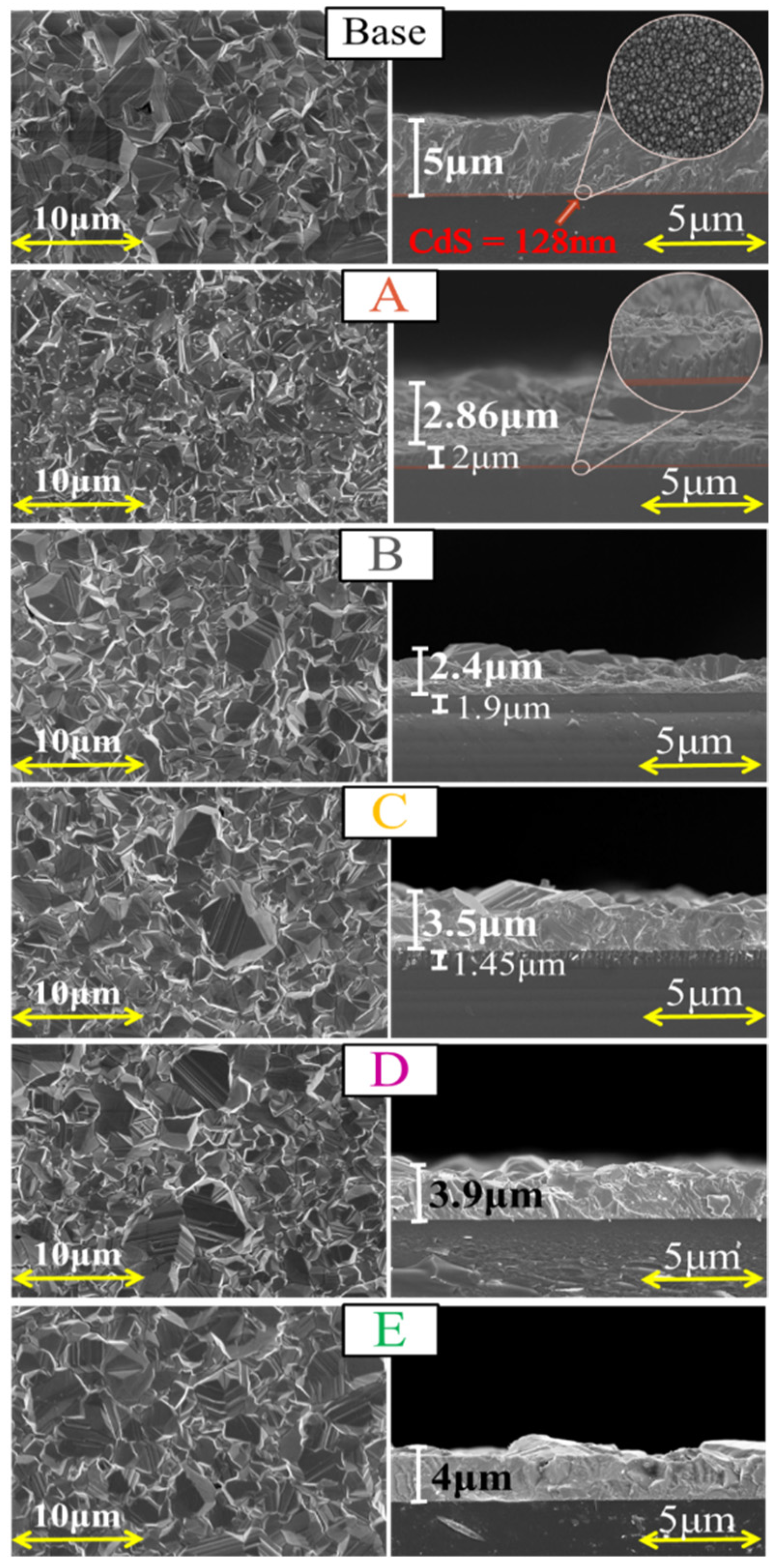
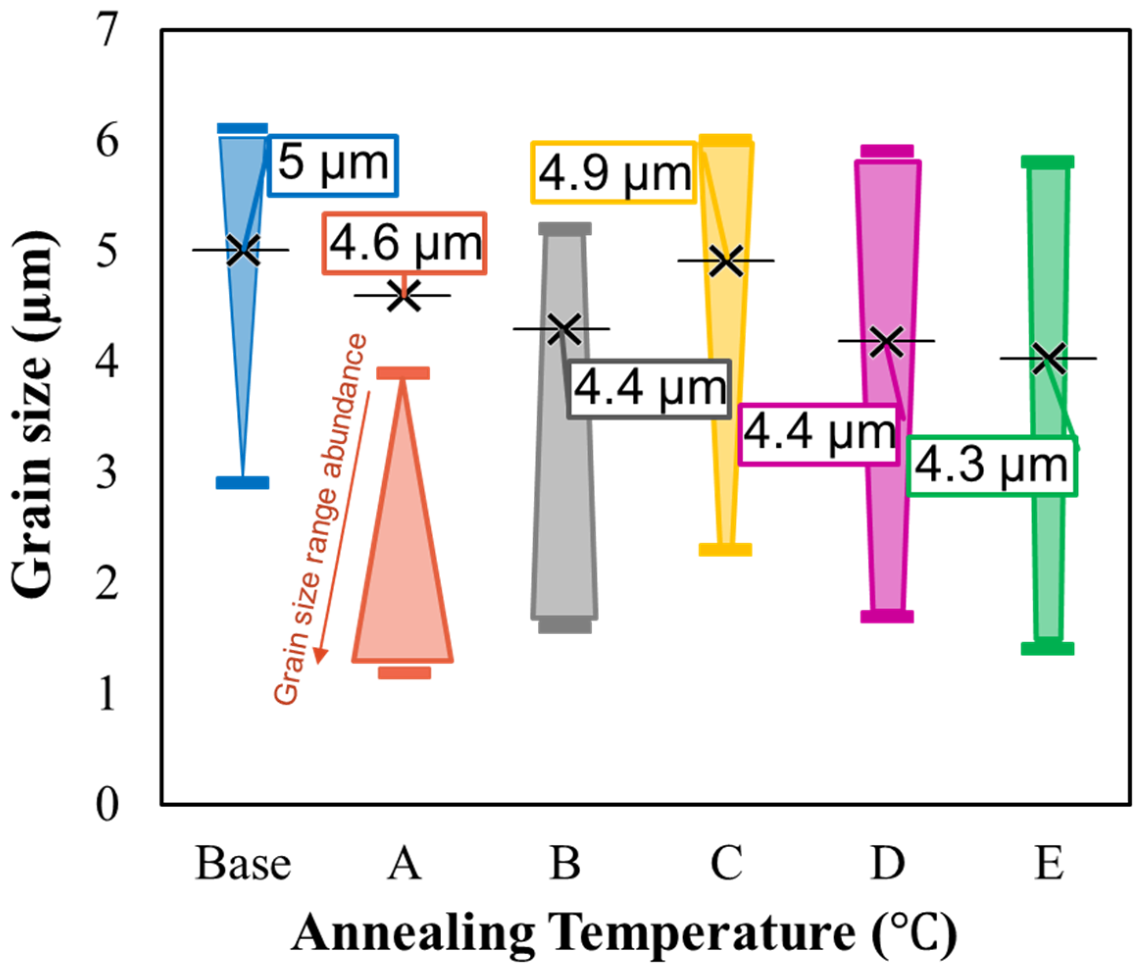
3.1. Surface Morphology by FESEM

Surface morphology analysis plays a substantial role in presenting the changes in the shape and size of the CdTe grains for as-deposited and CdCl2 -treated samples in the thickness range of few microns (~5 µm) [28]. From FESEM studies in Figure 4, the top view and cross-section results showed that the films had a column-shaped layout of clear non-cracking growth texture, which indicated the film quality. The general surface specifications of CdTe films did not alter to the extent of phase change; however, a consistent trend concerning the transformation in CdTe grain form was observed. The CdCl2 heat treatment facilitates grain boundary segregation, also classified as grain growth. This may be due to the recrystallization of CdTe during the heat treatment process, which lowered the atomic diffusion barrier at the CdTe grain boundaries. As a process of producing a liquid flux, the CdCl2 treatment approach recrystallizes the CdTe layer where some of the small grains coalesce into larger ones, while some of the larger grains split into smaller ones and reorient themselves, providing an entirely different microstructure [39]. CdTe crystallinity slowly increases during the heat treatment with CdCl2 due to the coalescing of crystalline nanoparticles, then a structural transition has been distinguished for the samples treated using higher temperatures (>390 °C) through a steady increase in temperature and crystalline grain boundary melting [40].
Impurities like Cd, Cl, and O in grains cause the CdTe crystals to continue as solids because of their high melting point of approximately 1093 °C. Hence, melting grain borders which start at around 375 °C are the main cause of the CdTe crystals to shift in orientations. The CdTe layer shifts from Te-rich to Cd-rich for samples annealed below (≤390 °C) because of CdCl2 heat treatment, which is the key point in the fabrication of high-performance cells [24]. The substance solidified afterward showing an enhancement at 390 °C in CdTe grain orientation. Relative intensities differ according to the heat treatment conditions. Grains develop primarily upward during heating due to Oswald ripening, and pinholes may form in higher annealing temperatures (<405 °C) resulting from the formation of large grains [41]. Therefore, at higher temperatures ~420 °C, film quality declines. The balance in growth rate between the crystallographic planes is a typical process causing roughness. To reduce the surface roughness, choosing the best treatment temperature range to alter the fastest growth direction is effective [42]. Figure 5 shows the changes in grain size for each treatment temperature.
Grain size usually refers to the average diameter of the individual crystal orientations found in polycrystalline materials. FESEM data represents the average grain size of the films to be highly dependent on the annealing temperature as a function of thickness. Presumably, fewer grain boundaries lead to reduced scattering and recombination of photogenerated carriers and the prevailing description is that Cl from the CdCl2 treatment segregates to grain boundaries, depleting or even inverting them with respect to grain interiors. Junctions between grain interiors and grain boundaries are expected to repel holes and conduct electrons to the back contact more efficiently [43]. Overall morphology results in this work imply that the films are uniform, smooth, homogeneous, and nearly dense-packed as well as free from voids, cracks, or pinholes. The smaller grain size in low treatment temperature happens as the consequence of insufficient heat for Te to turn into liquid although Cd is in liquid form at 360 °C, forming the vapor atoms during rapid film formation. This contributes to the formation of more atoms from which Cd-rich grains grow. Only at a higher annealing temperature of about 390 °C does the desorption of adatoms starts. Moreover, diffusion is much slower than adatoms because of surrounding surface atoms which result in forming the crater (layered hole) as in case A and B. Increasing the annealing temperature as for case C and D leads to the decrease in craters and then increases again for higher temperatures at 420 °C (case E). This suggests an incomplete treatment process in specific temperatures (below 390 °C) and over-heating when annealing temperatures >410 °C applied. Since, in the CSS deposition process, films go through a transition temperature (600 °C) and experience the highest possible grain nucleation stage, the thickness will not increase significantly during treatment [44,45]. From Figure 5. It is found that annealing temperature range 390–410 °C is suitable to improve spacing of the concentric atomic steps to form a uniform grain structure with improved symmetry for an increased minority carrier lifetime. In addition, topographic contrast of atomic steps can reveal phenomena related to attachment and detachment of atoms and qualify the film with respect to electrical properties. FESEM results agree with previous studies [42]. Grain boundary (GB) contrast is dark in untreated samples, suggesting high re-combination and bright contrast after treatment, as the effect of Cl in grain boundary passivation and electrical specs modification [46]. In total, ionization energy (IE = Evac − EVB) increased for treated samples, especially for samples B and E, with bright-lined grain boundaries [47].

3.2. Compositional Properties by EDX

EDX analysis was carried out to investigate the qualitative elemental analysis of the CdTe layer before and after the CdCl2 treatment. From research works based on semi-insulating CdTe, it is well known that Te precipitation forms in CdTe material, irrespective of the growth technique [48]. CdCl2 treatment and annealing remove these precipitated Te [25] that formed during the growth of CdTe due to the natural behavior of Te and known to cause the poor electronic quality of Ti-rich CdTe layers. As shown in Figure 6, Cd concentrations increase with the annealing temperature to about 380 °C with 49.60% Cd dominance. In cases A and B, the Cd peak increased between 0 to 2 keV and for films C and D, the Cd peak is presented to be in its highest intensity between 3 to 4 keV that reduced afterward for case E.
The higher intensity in Cd peak may be due to the reaction between Cd from CdCl2 and elemental Te to form CdTe or the excess Te sublimation and oxidized Te compounds during heat treatment using the optimum annealing temperature (~390 °C). On the other hand, the Te peak was observed to be in its highest intensity for case E, which is annealed at 420 °C. At a glance, the highest weightage of Te and Cd found in the samples at 420 °C and 375 °C temperature, respectively. From FESEM and EDX results, annealing temperature ranged 375–390 °C, yielding the stoichiometric CdTe layer, with more crystallinity and closer to Cd-rich samples, suitable for high-efficiency cell design.

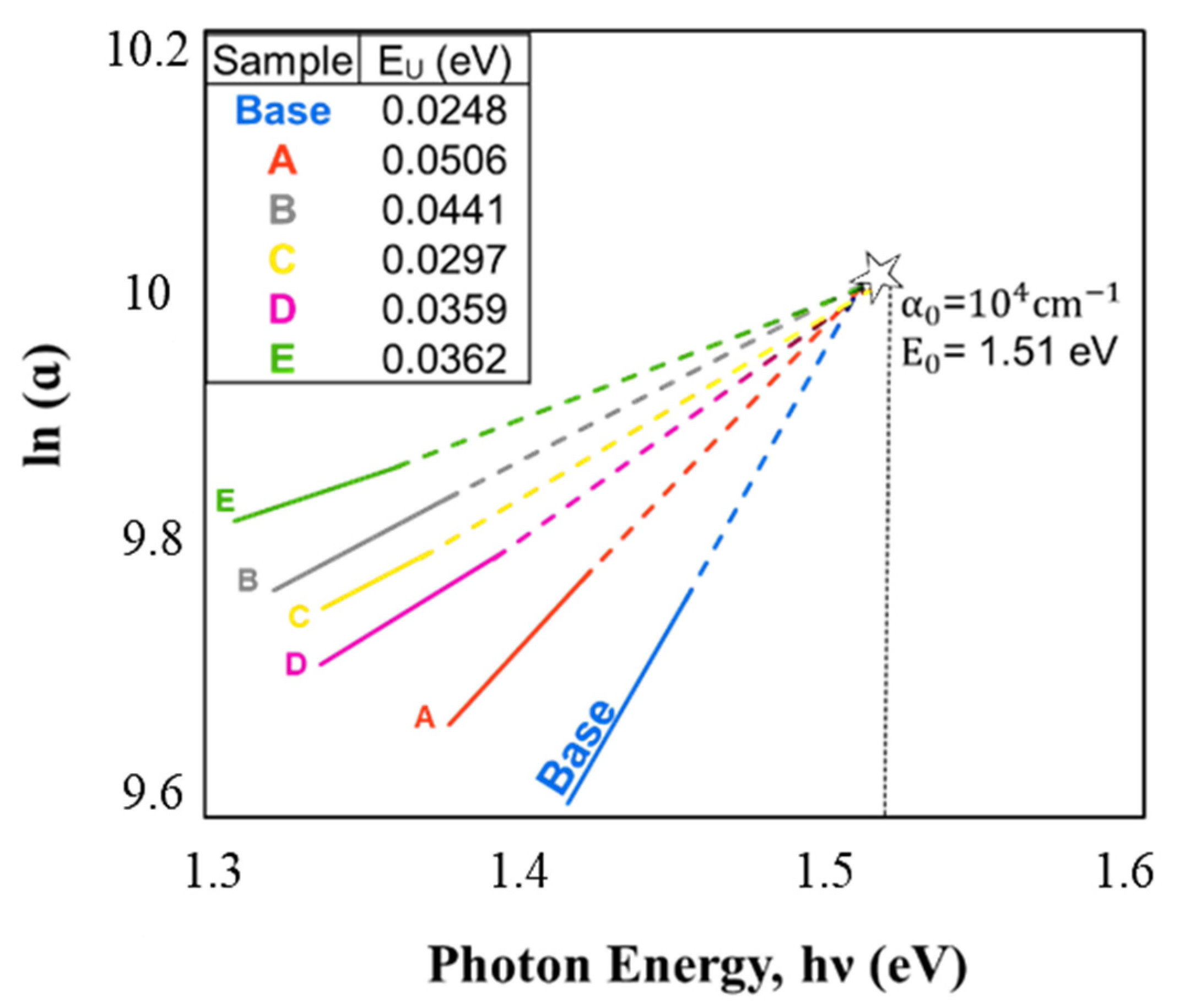
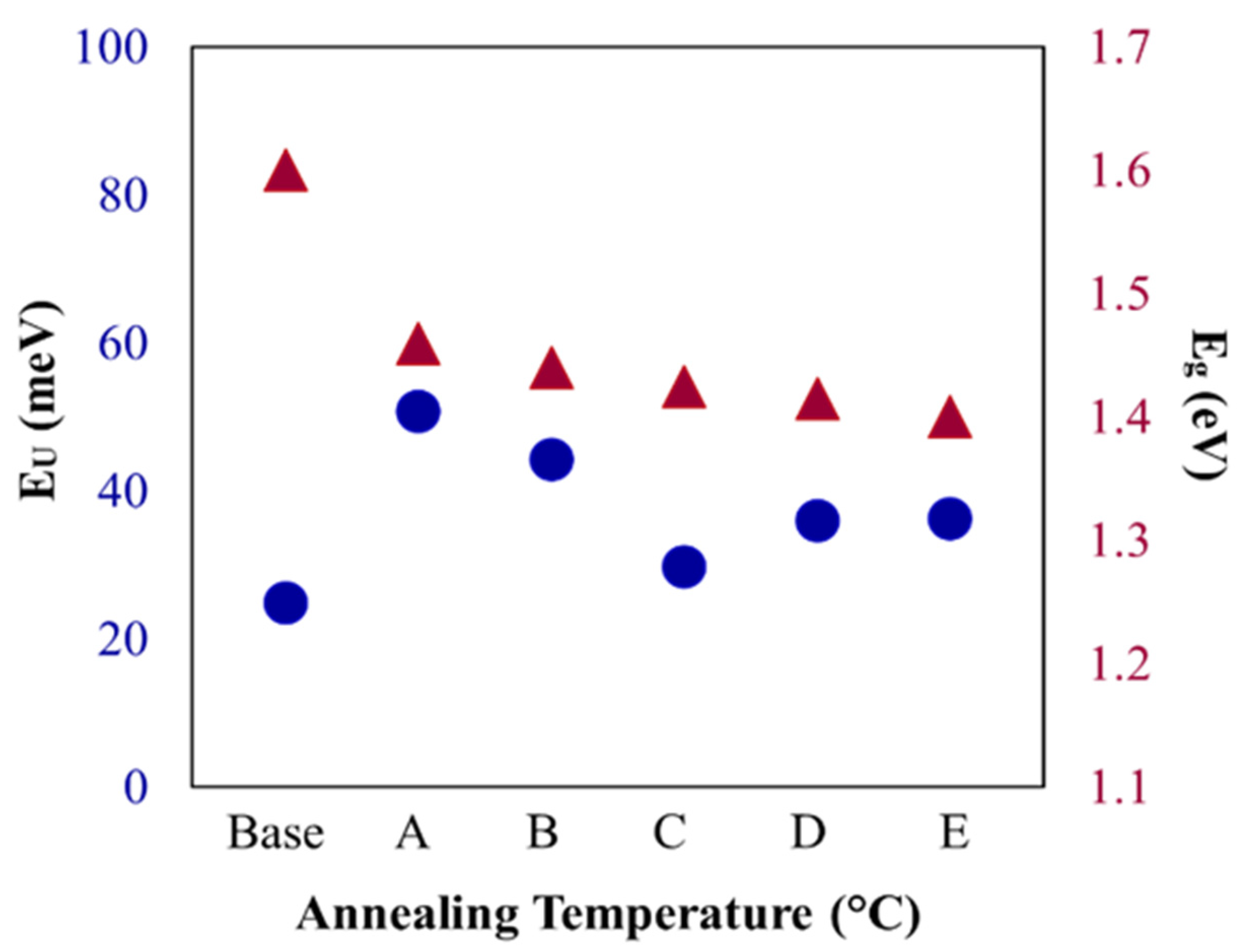
3.3. Optical Analysis

The energy band was calculated using the Tauc equation where the relation between absorption coefficient α and optical band gap Eg can be expressed as follows.
α h ν = K   ( h ν Eg ) n ,   when   α = 2.303   A t
where hν represents the photon energy which can be calculated by the following equation.
hν (eV) = 1.24/λ (µm)
where K is the electronic transition probability constant; t is the film thickness; A is the absorbance and power factor of n which is assumed to be ½ for direct bandgap materials [49]. Generally, bandgap in compounds can be modified through the stoichiometric deviations, grain boundary order, preferred orientation changes, as well as dislocation density and these factors, are the main characteristics of the films, targeted to improve using CdCl2 in this study. The optical band gap for treated CdTe was found in the range 1.4–1.5 eV, which was consistent with a report by Nima et al. [50]. It has been found that grain uniformity in the substrate, frontal layers, as well as CdTe layer before and after treatment have a direct effect on the optical energy gap (Eg). The reductions in the optical energy gap here from 1.6 to optimum 1.4 eV relates to greater CdTe thin films crystallinity and grain size, which in turn reduces the defect states or localized state intensity.
Chander et al. reported energy band gaps ranging from 1.6 to 1.7 for untreated samples due to the aforesaid deviation phenomenon in quantum scales [15]. From Figure 7, untreated CdTe film shows a band gap of 1.6 eV, which is higher than the bandgap for treated samples, in the range of 1.4 eV. This difference in the band energy value may be the result of better homogeneity and lower localized states [51]. For treated samples, the obtained bandgap range 1.39–1.46 eV may be the result of plasma frequency variation ascribed to the carrier density adjustments. Small changes in energy values for treated samples can be related to thermally excited impurity atoms in the bottom of the conduction band. Thickness dependency is another impactful factor on optical band energy for treated samples as reported by Khairnar et al. [52]. Moreover, the refractive index as a function of electronic polarizability, ionization, and local fields was calculated. From Table 4, the refractive index shows the lowest value 2.9 for baseline and is in the range from 2.97 to 3 for treated films.
The Refractive index portrays the effect of dislocation density [51] and increases while transmittance decreases slightly for treated films compared to untreated CdTe samples. No significant changes in the refractive index may be due to the same optical band gap and thickness for treated films. Besides, three critical phenomena occur in optical absorption spectra: (i) defect and impurities section (weak absorption), (ii) perturbation and disorder structural section (absorption edge), and (iii) the strong absorption section (optical energy gap) [53]. From Figure 8, changes in carrier concentration imputed to CdCl2 treatment affects the absorption coefficient near the band edge presented as the Urbach energy.
Urbach energy was estimated by plotting the ln α versus energy (hv) graph. The increase in α in the range of absorption edge or Urbach tail can be explained from transitions between the tails of the density of states in valance and conduction bands [38]. Additionally, the main factors of photon capture efficiency or phonon state disorders can be presented using Urbach energy changes [2]. The Urbach energy varies for each treated sample and the lowest deviation amount results from treated samples using 390 °C annealing temperature. Lower Urbach energy using electrical transitions between localized states can be a sign of orderly treated surface and better crystallinity in group C samples. Chandramohan et al. investigated CdTe designs using different types of substrates and reported that optical properties of CdTe thin films are directly related to substrate material used and its compatibility during the heat treatment process [54]. Salavei et al. applied a more concentrated CdCl2 solution to avoid the deviation of flexible substrate material and resultant inhomogeneity, as well as irreproducibility of the CdCl2 treatment step, yet efficiency loss was reported due to using opaque flexible substrates [31]. Here, the optimum treatment procedure applicable for CdTe superstrate design was proposed, and the final film’s results confirmed that high transparency and clarity properties of glass without any deformation or optical loss could be fabricated using UTG substrates. This verified the high potential of UTG glass for CdTe cell fabrication as stated in other work [55]. In addition, the absorption coefficient α0 is 104 cm−1 in the visible region proving that the desired absorbance over 90% for an efficient absorber layer. Figure 9 presents the relation between the band gap and Urbach tail. Band energy value is almost the same for all treated samples with around 2 eV lower amount from the untreated CdTe film. However, the Urbach energy has its highest value at 360 °C, and recommending this annealing temperature is not effective to reduce defects in CdTe films.

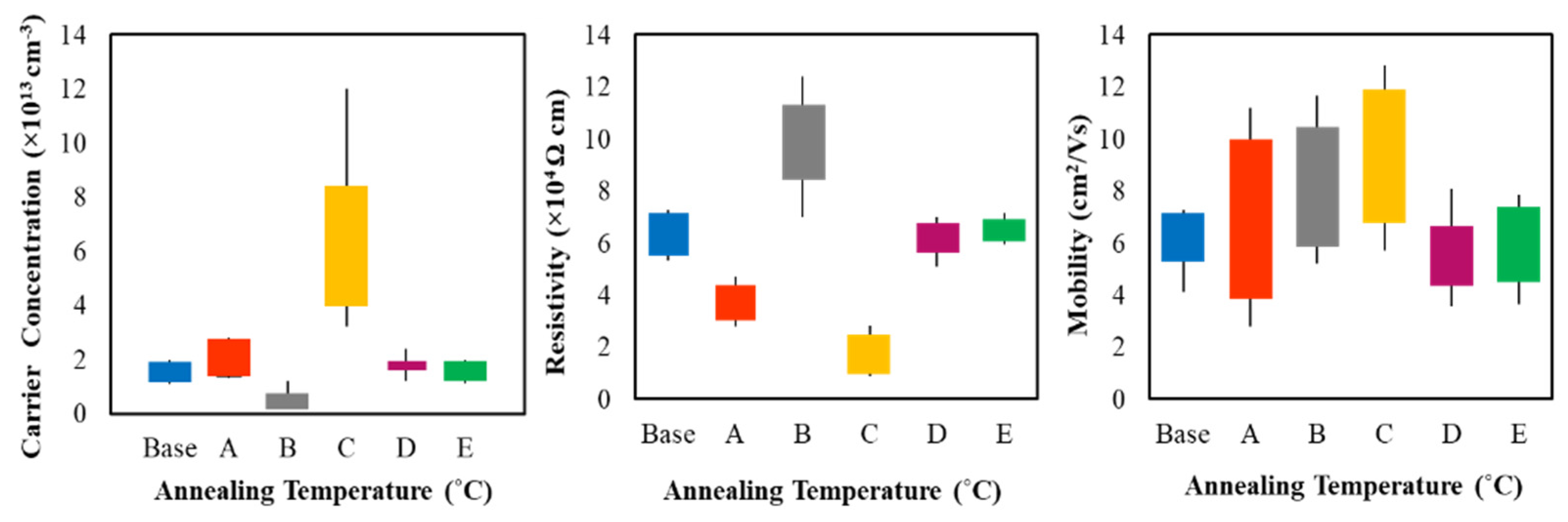
3.4. Electrical Properties

Carrier concentration, mobility, and the type of charge carriers were estimated using hall measurement. Hall calculation was proposed using current I = 45 nA in room temperature and all the films indicate p-type. The equations connecting the carrier concentration, mobility, and resistivity are represented as [σ = qημh] and [σ = 1/ρ] following ohm’s low, where σ is conductivity, ρ is resistivity, q is the electron charge, η is the electron density, and µh is the hall mobility. Carrier concentration is the number of free carriers present in the semiconductor and for p-type semiconductors, these free carriers are the number of holes in the valence band at thermal equilibrium. From Table 5, resistivity and carrier concentration are in the range of 104 Ω-cm and 1013 cm−3, respectively, in line with other studies [37,56]. The low carrier concentration is well known to be one of the efficiencies limiting factors in CdTe solar cells that will result in a steep C-V curve. Here, air ambient during the wet dipping process is proposed to improve carrier concentration value as stated in previous studies [57]. However, self-compensation of CdTe should be considered and other factors such as annealing temperature and annealing ambient are found to be highly effective that need to be optimized too. Mobility is referred to the velocity of electrons inside a semiconducting material in the presence of an electric field. Hence, levels of an impurity, defects, and carrier concentrations affect the mobility of carriers in a semiconductor. Mobility decreases for batch D and E, and for C samples, the highest carrier concentration is achieved indicating effective treatment to be around 390–405 °C.
CdTe has the drawback that it is difficult to achieve high doping concentration due to self-compensation from intrinsic defects form, e.g., vacancies (VCd, VTe), interstitial defects (Cdi, Tei), and grain boundaries [58]. Therefore, CdTe carrier concentration is found low, which is one of the key challenges to improve CdTe solar cells’ energy yield performance. It is therefore suggested that the choice of the optimum annealing temperature in the treatment process as a crucial stage has a notable impact on film properties. In this study using 390 °C as presented in Figure 10, crystallinity has improved and resulted in sample C with a slightly improved carrier concentration rate of 2 × 1014 cm−3. Aligning to the literature, we found that better crystallinity resulted in lower electrical resistivity, which was consistent with this study as well. This was mainly due to reduced carrier scattering and recombination across the grain boundaries (GB). Figure 10 and Figure 11 confirm the reduction of carrier scattering at grain boundaries and increase in mobility for annealed samples using temperature below 405 °C, like other studies by reference [59].
Electrical property among grain boundaries is essential to clarify the optimum treatment temperature for CdTe thin film. Aligning with the literature, it is confirmed that surface uniformity and improved boundaries result in lower electrical resistivity resulted from sample C, mostly because of lower carrier dispersion and recombination through grain boundaries consistent with other studies [37]. However, the Hall measurement alone is not a widespread calculation to resemble the electrical property endorsement of CdTe concerning the post-deposition treatment. It is credible to accomplish more characterization analysis in the future that would possibly confer more strong features.

4. Conclusions

The influence of CdCl2 treatment in CdTe thin film is discussed and investigated thoroughly using various characterization tools. Analyzed results verify the temperature dependence for grain growth. For samples treated approximately at 390 °C with CdTe grain size ranging between 2 to 6 μm, the film surface morphology is clear, tightly packaged, and free of visible crystal defects. The optical transition was direct in nature, and the bandgap was observed in the range of 1.39–1.46 eV after treatment. The film treated at 390 °C resulted in the highest carrier concentration and mobility. Morphology and crystal orientation validate the quality of the thin films unaffected for UTG (100 μm) used as substrate. This study verified the UTG substrate survived the optimum treatment temperature needed for CdTe films and no deformation or structural changes happened during the subsequent CdCl2 treatment process. The optimized results for CdTe film thickness of around 5 µm with uniform grain growth after CdCl2 treatment are found showing resistivity of 104 Ω-cm, carrier concentration of 1013 cm−3, the band gap of 1.4 eV, the absorption coefficient of 104 cm−3, and optimum CdS thickness of 130 nm. The optimum results demonstrate that the CdCl2 treatment temperature within the range of 390–405 °C might be considered as the optimum temperature for the fabrication of CdTe solar cell on UTG substrate via CSS method.

Author Contributions

Conceptualization, N.A.; data curation, N.A.; formal Analysis, N.A.; funding acquisition, Z.A.A.; methodology, N.A.; investigation, N.A.; project administration, N.A., M.R.K., and Z.A.A.; writing—original draft preparation, N.A.; writing—review and editing, N.A.; visualization, M.R.K. and Z.A.A.; validation, N.A.; supervision, N.A., M.R.K., and Z.A.A. All authors have read and agreed to the published version of the manuscript.

Funding

This project was funded by the National Plan for Science, Technology, and Innovation (MAARIFAH), King Abdul Aziz City for Science and Technology, Kingdom of Saudi Arabia, with award number 13-ENE2229-02.

Institutional Review Board Statement

Not applicable.

Informed Consent Statement

Not applicable.

Data Availability Statement

Not applicable.

Acknowledgments

Authors acknowledge the National Plan for Science, Technology, and Innovation (MAARIFAH), King Abdulaziz City for Science and Technology, Kingdom of Saudi Arabia for its grant with award number 13-ENE2229-02.

Conflicts of Interest

The authors declare no conflict of interest.

References

  1. Fang, X.; Ren, S.; Li, C.; Li, C.; Chen, G.; Lai, H.; Zhang, J.; Wu, L. Investigation of recombination mechanisms of CdTe solar cells with different buffer layers. Sol. Energy Mater. Sol. Cells 2018, 188, 93–98. [Google Scholar] [CrossRef]
  2. Islam, M.A.; Rahman, K.S.; Sobayel, K.; Enam, T.; Ali, A.M.; Zaman, M.; Akhtaruzzaman, M.; Amin, N. Fabrication of high efficiency sputtered CdS: O/CdTe thin film solar cells from window/absorber layer growth optimization in magnetron sput-tering. Sol. Energy Mater. Sol. Cells 2017, 172, 384–393. [Google Scholar] [CrossRef]
  3. Oluyamo, S.S.; Akinboyewa, L.O.; Fuwape, I.A.; Olusola, O.I.O.; Adekoya, M.A. Influence of nanocellulose concentration on the tunability of energy bandgap of cadmium telluride thin films. Cellulose 2020, 27, 8147–8153. [Google Scholar] [CrossRef]
  4. Doroody, C.; Rahman, K.; Abdullah, S.; Harif, M.; Rosly, H.; Tiong, S.; Amin, N. Temperature difference in close-spaced sub-limation (CSS) growth of CdTe thin film on ultra-thin glass substrate. Results Phys. 2020, 18, 103213. [Google Scholar] [CrossRef]
  5. Le Bourhis, E. Glass: Mechanics and Technology; John Wiley & Sons: Weinheim, Germany, 2014. [Google Scholar]
  6. Ho, S.M. Synthesis of Thin Films on Flexible Substrates: A Review. Middle-East. J. Sci. Res. 2016, 24, 2235–2238. [Google Scholar]
  7. Paul, S.; Swartz, C.; Sohal, S.; Grice, C.; Bista, S.S.; Li, D.-B.; Yan, Y.; Holtz, M.; Li, J.V. Buffer/absorber interface recombination reduction and improvement of back-contact barrier height in CdTe solar cells. Thin Solid Film. 2019, 685, 385–392. [Google Scholar] [CrossRef]
  8. Song, T.; Kanevce, A.; Sites, J.R. Emitter/absorber interface of CdTe solar cells. J. Appl. Phys. 2016, 119, 233104. [Google Scholar] [CrossRef]
  9. Amarasinghe, M.; Colegrove, E.; Moseley, J.; Moutinho, H.; Albin, D.; Duenow, J.; Jensen, S.; Kephart, J.; Sampath, W.; Si-vananthan, S.; et al. Obtaining large columnar CdTe grains and long lifetime on nanocrystalline CdSe, MgZnO, or CdS layers. Adv. Energy Mater. 2018, 8, 1702666. [Google Scholar] [CrossRef]
  10. Abbas, A.; West, G.D.; Bowers, J.W.; Kaminski, P.M.; Maniscalco, B.; Walls, J.M.; Barth, K.L.; Sampath, W.S. Cadmium chloride assisted re-crystallization of CdTe: The effect of varying the annealing time. Mrs Online Proc. Libr. Arch. 2014, 1638, 1–6. [Google Scholar] [CrossRef]
  11. McCandless, B.; Metzger, W.K.; Buchanan, W.; Sriramagiri, G.; Thompson, C.; Duenow, J.; Albin, D.; Jensen, S.A.; Moseley, J.; Al-Jassim, M. Enhanced p-Type Doping in Polycrystalline CdTe Films: Deposition and Activation. IEEE J. Photovolt. 2019, 9, 912–917. [Google Scholar] [CrossRef]
  12. Awni, R.A.; Li, D.B.; Song, Z.; Bista, S.S.; Razooqi, M.A.; Grice, C.R.; Chen, L.; Liyanage, G.K.; Li, C.; Phillips, A.B.; et al. In-fluences of buffer material and fabrication atmosphere on the electrical properties of CdTe solar cells. Prog. Photovolt. Res. Appl. 2019, 27, 1115–1123. [Google Scholar] [CrossRef]
  13. Schuler, G.P.; Maniscalco, B.; Bowers, J.W.; Claudio, G.; M, J. Walls Optimisation of Cadmium Chlo-Ride Solution Processing of Close Space Sublimated Thin Film CdTe Solar Cells. 2013. pp. 175–178. Available online: https://repository.lboro.ac.uk/articles/conference_contribution/Optimisation_of_cadmium_chloride_solution_processing_of_close_space_sublimated_thin_film_CdTe_solar_cells/9556787/1 (accessed on 22 February 2021).
  14. Bai, Z.; Wan, L.; Hou, Z.; Wang, D. Effect of CdCl2 annealing treatment on CdS thin films and CdTe/CdS thin film solar cells. Phys. Status Solidi 2010, 8, 628–630. [Google Scholar] [CrossRef]
  15. Chander, S.; Dhaka, M.S. CdCl2 treatment concentration evolution of physical properties correlation with surface morphology of CdTe thin films for solar cells. Mater. Res. Bull. 2018, 97, 128–135. [Google Scholar] [CrossRef]
  16. Abbas, A.; West, G.D.; Bowers, J.W.; Isherwood, P.; Kaminski, P.M.; Maniscalco, B.; Rowley, P.; Walls, J.M.; Barricklow, K.; Sampath, W.S.; et al. The effect of cadmium chloride treatment on close spaced sublimated cadmium telluride thin film solar cells. In Proceedings of the 2012 IEEE 38th Photovoltaic Specialists Conference (PVSC) PART 2, Austin, TX, USA, 3–8 June 2012; pp. 1–6. [Google Scholar]
  17. Kim, M.; Sohn, S.; Lee, S. Reaction kinetics study of CdTe thin films during CdCl2 heat treatment. Sol. Energy Mater. Sol. Cells 2011, 95, 2295–2301. [Google Scholar] [CrossRef]
  18. Moutinho, H.R.; Al-Jassim, M.M.; Levi, D.H.; Dippo, P.C.; Kazmerski, L.L. Effects of CdCl2 treatment on the recrystallization and electro-optical properties of CdTe thin films. J. Vac. Sci. Technol. A: Vac. Surf. Film. 1998, 16, 1251–1257. [Google Scholar] [CrossRef]
  19. Li, C.; Poplawsky, J.; Wu, Y.; Lupini, A.R.; Mouti, A.; Leonard, D.N.; Paudel, N.; Jones, K.; Yin, W.; Al-Jassim, M.; et al. From atomic structure to photovoltaic properties in CdTe solar cells. Ultramicroscopy 2013, 134, 113–125. [Google Scholar] [CrossRef]
  20. Chander, S.; Dhaka, M. Time evolution to CdCl2 treatment on Cd-based solar cell devices fabricated by vapor evaporation. Sol. Energy 2017, 150, 577–583. [Google Scholar] [CrossRef]
  21. Samoilenko, Y.; Yeung, G.; Munshi, A.H.; Abbas, A.; Reich, C.L.; Walker, M.; Reese, M.O.; Zakutayev, A.; Walls, J.M.; Sampath, W.S.; et al. Stable magnesium zinc oxide by reactive Co-Sputtering for CdTe-based solar cells. Sol. Energy Mater. Sol. Cells 2020, 210, 110521. [Google Scholar] [CrossRef]
  22. Jain, G.; Ahnood, A.; Chanaewa, A.; Fox, K.; Mulvaney, P. The role of CdCl2 treatments and annealing in the formation of sintered CdTe nanocrystal solar cells. Phys. Lett. A 2019, 383, 1199–1202. [Google Scholar] [CrossRef]
  23. Wang, L.; Luo, M.; Qin, S.; Liu, X.; Chen, J.; Yang, B.; Leng, M.; Xue, D.-J.; Zhou, Y.; Gao, L.; et al. Ambient CdCl2 treatment on CdS buffer layer for improved performance of Sb2Se3 thin film photovoltaics. Appl. Phys. Lett. 2015, 107, 143902. [Google Scholar] [CrossRef]
  24. Willeke, G.P.; Weber, E.R. Advances in Photovoltaics: Part 2; Newnes: Oxford, UK, 17 October 2013. [Google Scholar]
  25. Harvey, S.P.; Teeter, G.; Moutinho, H.; Al-Jassim, M.M. Direct evidence of enhanced chlorine segregation at grain boundaries in polycrystalline CdTe thin films via three-dimensional TOF-SIMS imaging. Prog. Photovolt. Res. Appl. 2015, 23, 838–846. [Google Scholar] [CrossRef]
  26. AbuEl-Rub, K.M.; Hahn, S.R.; Tari, S.; Dissanayake, M.A.K.L. Effects of CdCl2 heat treatment on the morphological and chemical properties of CdTe/CdS thin films solar cells. Appl. Surf. Sci. 2012, 258, 6142–6147. [Google Scholar] [CrossRef]
  27. Dharmadasa, I.M.; Ojo, A.A. Unravelling complex nature of CdS/CdTe based thin film solar cells. J. Mater. Sci. Mater. Electron. 2017, 28, 16598–16617. [Google Scholar] [CrossRef] [Green Version]
  28. Dharmadasa, I.M. Review of the CdCl2 Treatment Used in CdS/CdTe Thin Film Solar Cell Development and New Evidence towards Improved Understanding. Coatings 2014, 4, 282–307. [Google Scholar] [CrossRef]
  29. Romeo, N.; Bosio, A.; Tedeschi, R.; Romeo, A.; Canevari, V. A highly efficient and stable CdTe/CdS thin film solar cell. Sol. Energy Mater. Sol. Cells 1999, 58, 209–218. [Google Scholar] [CrossRef]
  30. Hajimammadov, R.; Fathi, N.; Bayramov, A.; Khrypunov, G.; Klochko, N.; Li, T. Effect of ‘CdCl2 Treatment’ on properties of CdTe-based solar cells prepared by physical vapor deposition and close-spaced sublimation methods. Jpn. J. Appl. Phys. 2011, 50, 05FH01. [Google Scholar] [CrossRef]
  31. Salavei, A.; Rimmaudo, I.; Piccinelli, F.; Menossi, D.; Romeo, N.; Bosio, A.; Dharmadasa, R.; Romeo, A. Flexible CdTe solar cells by a low temperature process on ITO/ZnO coated polymers. In Proceedings of the 27th European Photovoltaic Solar Energy Conference and Exhibition, Frankfurt, Germany, 24 September 2012; pp. 24–28. [Google Scholar]
  32. Major, J.D.; Al Turkestani, M.; Bowen, L.; Brossard, M.; Li, C.; Lagoudakis, P.; Pennycook, S.J.; Phillips, L.J.; Treharne, R.E.; DuRose, K. In-depth analysis of chloride treatments for thin-film CdTe solar cells. Nat. Commun. 2016, 7, 13231. [Google Scholar] [CrossRef] [Green Version]
  33. Dharmadasa, I.M.; Echendu, O.K.; Fauzi, F.; Abdul-Manaf, N.A.; Olusola, O.I.; Salim, H.I.; Madugu, M.L.; Ojo, A.A. Im-provement of composition of CdTe thin films during heat treatment in the presence of CdCl2. J. Mater. Sci. Mater. Electron. 2017, 28, 2343–2352. [Google Scholar] [CrossRef] [Green Version]
  34. Ulmer, M.P.; Graham, M.E.; Vaynman, S.; Cao, J.; Takacs, P.Z. Magnetic smart material application to adaptive x-ray optics. In Adaptive X-ray Optics; International Society for Optics and Photonics: San Diego, CA, USA, 2010; Volume 7803, p. 780309. [Google Scholar]
  35. Ottermann, C.; Sparschuh, G. Process for Producing Organic Light-Emitting Devices. U.S. Patent Application 10/556,752, 29 November 2007. [Google Scholar]
  36. Osedach, T.P.; Geyer, S.M.; Ho, J.C.; Arango, A.C.; Bawendi, M.G.; Bulović, V. Lateral heterojunction photodetector consisting of molecular organic and colloidal quantum dot thin films. Appl. Phys. Lett. 2009, 94, 26. [Google Scholar] [CrossRef]
  37. Rahman, K.S.; Harif, M.N.; Rosly, H.N.; Kamaruzzaman, M.I.B.; Akhtaruzzaman, M.; Alghoul, M.; Misran, H.; Amin, N. Influence of deposition time in CdTe thin film properties grown by Close-Spaced Sublimation (CSS) for photovoltaic applica-tion. Results Phys. 2019, 14, 102371. [Google Scholar] [CrossRef]
  38. Romeo, A.; Arnold, M.; Bätzner, D.L.; Zogg, H.; Tiwari, A. Development of high efficiency flexible CdTe solar cells. In Proceedings of the PV in Europe from PV Technology to Energy Solutions Conference and Exhibition, Rome, Italy, 7 October 2002; pp. 377–381. [Google Scholar]
  39. Harif, M.N.; Rahman, K.S.; Rosly, H.N.; Chelvanathan, P.; Doroody, C.; Misran, H.; Amin, N. An approach to alternative post-deposition treatment in CdTe thin films for solar cell application. Superlattices Microstruct. 2020, 147, 106687. [Google Scholar] [CrossRef]
  40. Dharmadasa, I.M.; Bingham, P.A.; Echendu, O.K.; Salim, H.I.; Druffel, T.; Dharmadasa, R.; Sumanasekera, G.U.; Dharmasena, R.R.; Dergacheva, M.B.; Mit, K.A.; et al. Fabrication of CdS/CdTe-based thin film solar cells using an electrochemical technique. Coatings 2014, 4, 380–415. [Google Scholar] [CrossRef]
  41. Munshi, A.H.; Kephart, J.M.; Abbas, A.; Danielson, A.; Gḗlinas, G.; Beaudry, J.-N.; Barth, K.L.; Walls, J.M.; Sampath, W.S. Effect of CdCl2 passivation treatment on microstructure and performance of CdSeTe/CdTe thin-film photovoltaic devices. Sol. Energy Mater. Sol. Cells 2018, 186, 259–265. [Google Scholar] [CrossRef] [Green Version]
  42. Kajikawa, Y. Analysing surface roughness evolution in thin films. In Thin Film Growth; Woodhead Publishing: Cambridge, UK, 2011; pp. 60–82. [Google Scholar]
  43. Berg, M.; Kephart, J.M.; Sampath, W.S.; Ohta, T.; Chan, C. Effects of CdCl2 treatment on the local electronic properties of polycrystalline CdTe measured with photoemission electron microscopy. In Proceedings of the 2017 IEEE 44th Photovoltaic Specialist Conference (PVSC), Washington, DC, USA, 25–30 June 2017; pp. 3417–3421. [Google Scholar]
  44. Major, J.D. Grain boundaries in CdTe thin film solar cells: A review. Semicond. Sci. Technol. 2016, 31, 093001. [Google Scholar] [CrossRef]
  45. Amin, N.; Rahman, K.S. Close-Spaced Sublimation (CSS): A Low-Cost, High-Yield Deposition System for Cadmium Telluride (CdTe) Thin Film Solar Cells. Mod. Technol. Creat. Thin-Film Syst. Coat. 2017, 361, 361–380. [Google Scholar]
  46. Li, C.; Wu, Y.; Poplawsky, J.; Pennycook, T.J.; Paudel, N.; Yin, W.; Haigh, S.J.; Oxley, M.P.; Lupini, A.R.; Al-Jassim, M.; et al. Grain-Boundary-Enhanced Carrier Collection in CdTe Solar Cells. Phys. Rev. Lett. 2014, 112, 156103. [Google Scholar] [CrossRef]
  47. Berg, M.; Kephart, J.M.; Munshi, A.; Sampath, W.S.; Ohta, T.; Chan, C. Local Electronic Structure Changes in Polycrystalline CdTe with CdCl2 Treatment and Air Exposure. ACS Appl. Mater. Interfaces 2018, 10, 9817–9822. [Google Scholar] [CrossRef] [Green Version]
  48. Ayoub, M.; Hage-Ali, M.; Koebel, J.M.; Zumbiehl, A.; Klotz, F.; Rit, C.; Regal, R.; Fougeres, P.; Siffert, P. Annealing effects on defect levels of CdTe: Cl materials and the uniformity of the electrical properties. IEEE Trans. Nucl. Sci. 2003, 50, 229–237. [Google Scholar] [CrossRef]
  49. Shaaban, E.; Afify, N.; El-Taher, A. Effect of film thickness on microstructure parameters and optical constants of CdTe thin films. J. Alloy. Compd. 2009, 482, 400–404. [Google Scholar] [CrossRef]
  50. Gorji, N.E. Deposition and doping of CdS/CdTe thin film solar cells. J. Semicond. 2015, 36, 54001. [Google Scholar] [CrossRef]
  51. Maxwell, G.L. Characterization and Modeling of CdCl2 Treated CdTe/CdS Thin-Film Solar Cell. Ph.D. Thesis, Colorado State University, Fort Collins, CO, USA, 2010. [Google Scholar]
  52. Khairnar, U.P.; Bhavsar, D.S.; Vaidya, R.U.; Bhavsar, G.P. Optical properties of thermally evaporated cadmium telluride thin films. Mater. Chem. Phys. 2003, 80, 421–427. [Google Scholar] [CrossRef]
  53. Hasaneen, M.; Alrowaili, Z.A.; Mohamed, W. Structure and optical properties of polycrystalline ZnSe thin films: Validity of Swanepol’s approach for calculating the optical parameters. Mater. Res. Express 2020, 7, 016422. [Google Scholar] [CrossRef]
  54. Chandramohan, S.; Sathyamoorthy, R.; Lalitha, S.; Senthilarasu, S. Structural properties of CdTe thin films on different sub-strates. Sol. Energy Mater. Sol. Cells 2006, 90, 686–693. [Google Scholar] [CrossRef]
  55. Cho, E.; Kang, Y.; Kim, D. Post-growth process for flexible CdS/CdTe thin film solar cells with high specific power. Opt. Express 2016, 24, A791–A796. [Google Scholar] [CrossRef] [PubMed]
  56. Gu, H.; Ren, A.; Zhang, J.; Li, K.; Li, C.; Wang, W.; Xu, H. The study of oxygen concentration in the CdTe thin film prepared by vapor transport deposition for CdTe photovoltaic devices. J. Mater. Sci. Mater. Electron. 2017, 28, 9442–9449. [Google Scholar] [CrossRef]
  57. Regalado-Perez, E.; Reyes-Banda, M.G.; Mathew, X. Influence of oxygen concentration in the CdCl2 treatment process on the photovoltaic properties of CdTe/CdS solar cells. Thin Solid Film. 2015, 582, 134–138. [Google Scholar] [CrossRef]
  58. McCandless, B.E.; Buchanan, W.A.; Thompson, C.P.; Sriramagiri, G.; Lovelett, R.J.; Duenow, J.; Albin, D.; Jensen, S.; Colegrove, E.; Moseley, J.; et al. Overcoming Carrier Concentration Limits in Polycrystalline CdTe Thin Films with In Situ Doping. Sci. Rep. 2018, 8, 1–13. [Google Scholar] [CrossRef] [Green Version]
  59. Rahman, K.S.; Haque, F.; Khan, N.A.; Islam, M.A.; Alam, M.M.; Alothman, Z.A.; Sopian, K.; Amin, N. Effect of CdCl2 treatment on thermally evaporated CdTe thin films. Chalcogenide Lett. 2014, 11, 129–139. [Google Scholar]
Figure 1. Schematic view of CdTe solar cell structure with a post-annealing temperature range.
Crystals 11 00390 g001
Figure 2. Schematic of the complete process of film preparation, (1) Glass preparation, (2) substrate cleaning, (3) Substrate drying, (4) ITO/CdS sputtering, (5) CdTe Sublimation, (6) Glass/ITO/CdS/CdTe.
Crystals 11 00390 g002
Figure 3. Schematic illustration of the sequential CdCl2 treatment, (1) Solution preparation, (2) Wet CdCl2 treatment, (3) Post treatment annealing, (4) Residuals removal by warm DI water.
Crystals 11 00390 g003
Figure 4. Surface morphology, top view (left figures) and cross-section views (right figures) of the base and CdCl2 treated CdTe thin films obtained by FESEM.
Crystals 11 00390 g004
Figure 5. Grain size variation for CdTe films for different temperatures.
Crystals 11 00390 g005
Figure 6. EDX spectra of CdTe thin films.
Crystals 11 00390 g006
Figure 7. Tauc plot for the determination of bandgap of CdTe films before and after treatment.
Crystals 11 00390 g007
Figure 8. Urbach energy determination of CdTe film.
Crystals 11 00390 g008
Figure 9. The relation between the bandgap energy and the Urbach tail of CdTe films.
Crystals 11 00390 g009
Figure 10. The Hall effect results for CdTe films before and after treatment.
Crystals 11 00390 g010
Figure 11. Changes in electrical parameters of CdTe thin film for various annealing temperatures.
Crystals 11 00390 g011
Table 1. Deposition parameters of sputtered ITO and CdS layers.
ParameterITO LayerCdS Layer
ModeDCRF
Substrate TemperatureAmbientAmbient
Deposition Time (mins)4010
Power (W)5040
Argon Flow Rate (SCCM)45
Base Pressure (Torr)10−510−5
Operating Pressure (mTorr)2518
Table 2. Growth parameters for CSS deposited CdTe films.
ParameterCondition
Substrate Temperature500 °C
Source Temperature600 °C
Argon Flow Rate1–1.5 Torr
Source-Substrate Distance1 mm
Deposition Time 10 min
Ambient GasArgon
Table 3. Simplified sample name for different annealing temperatures.
Sample ID#Annealing Temperature (°C)
Base-
A360
B375
C390
D405
E420
Table 4. Optical parameters of CdTe thin film for various annealing temperatures.
SampleBand Gap, Eg (eV)Urbach Energy, EU (meV)Refractive Index (n)
Base1.624.802.90
A1.4650.682.97
B1.4444.172.98
C1.42529.752.99
D1.41535.953.00
E1.3936.293.00
Table 5. Electrical properties of CdTe film for various annealing temperatures.
SampleCarrier Concentration
[×1013] (/cm3)
Mobility
(cm2/Vs)
Resistivity
[×104] (Ω-cm)
Base1.40926.57536.7451
A2.32457.15713.7567
B0.70987.181111.2617
C6.98498.76501.0208
D1.81415.33886.453
E1.81145.49546.2786
Publisher’s Note: MDPI stays neutral with regard to jurisdictional claims in published maps and institutional affiliations.

