Abstract
Copper oxide (CuxO) films are considered to be an attractive hole-transporting material (HTM) in the inverted planar heterojunction perovskite solar cells due to their unique optoelectronic properties, including intrinsic p-type conductivity, high mobility, low-thermal emittance, and energy band level matching with the perovskite (PS) material. In this study, the potential of reactive sputtered CuxO thin films with a thickness of around 100 nm has been extensively investigated as a promising HTM for effective and stable perovskite solar cells. The as-deposited and annealed films have been characterized by using X-ray Diffraction (XRD), Scanning Electron Microscopy (SEM), Photoluminescence (PL), UV-Vis spectroscopy, and Hall-effect measurement techniques. The significant change in structural and optoelectronic properties has been observed as an impact of the thermal annealing process. The phase conversion from Cu2O to CuO, including grain size increment, was observed upon thermal annealing. The transmittance and optical bandgap were found to vary with the films’ crystallographic transformation. The predominant p-type conductivity and optimum annealing time for higher mobility have been confirmed from the Hall measurement. Films’ optoelectrical properties were implemented in the complete perovskite solar cell for numerical analysis. The simulation results show that a 40 min annealed CuxO film yields the highest efficiency of 22.56% with a maximum open-circuit voltage of 1.06 V.
1. Introduction
A significant recent discovery in the field of photovoltaics is known to be organic–inorganic perovskite solar cells (PSCs) [1]. It has attracted much more attention because it showed the best alternative approach for replacing the costly crystalline silicon solar cells [2,3,4,5]. Remarkably, by improving the desired optoelectronic properties utilizing device engineering and material design, the recorded power conversion efficiency (PCE) of PSCs has already been raised from 3.1% to 25.2% in only 10 years of duration [6]. However, achieving long-term stability in PSC remains a big challenge. PSCs are typically prone to decay when exposed to humidity, oxygen, heat, and/or light etc., which must be solved for practical applications. It should be noticed that among the several causes, the nature of hole-transporting materials (HTMs) have a big influence on PSCs instability. Currently, organic–inorganic Poly(3,4-ethylenedioxythiophene)-poly(styrenesulfonate) (PEDOT: PSS) and 2,2′,7,7′-Tetrakis[N,N-di(4-methoxyphenyl)amino]-9,9′-spirobifluorene (Spiro-OMeTED) are commonly used as the HTM in heterojunction PSCs due to their conformity and high performance [7]. However, both materials are expensive, and their fabrication technique is complex. Also, their acidity degrades the perovskite layer, which ultimately affects cell stability [8]. For solving the above issues, inorganic p-type materials as the hole transport layer (HTL) has been proposed by several researchers that have already shown excellent chemical stability. Also, fabricating inorganic HTM is simpler than the commonly used organic HTM [9,10].
Some inorganic HTLs, such as nickel oxide (NiO) [11], copper thiocyanate (CuSCN) [12], copper iodide (CuI) [13], graphene oxide (GO) [14], and copper oxide CuxO (CuO or Cu2O) [15] have already attracted significant interest because of their suitable optoelectronic properties for high-efficiency solar cell application [16]. It should be noticed that among them, CuxO has versatile applications, including superconductors, sensors, and even as an absorber layer in solar cells. Also, CuxO can create a very good ohmic contact between the perovskite layer and the anode, which certainly enhances the carrier transportation to the load. Also, CuxO thin films can be prepared by various low-cost and simple methods, including successive ionic-layer adsorption and reaction (SILAR) method [17], electrochemical deposition [18,19], thermal oxidation [20], chemical dissolution [21], and reactive sputtering [22]. Despite its various advantages in PSC applications, the highest efficiency of PSC with a CuxO HTL was reported at only about 17% [23], which is significantly lower than the efficiency achieved with organic HTM, indicating the vital importance of more study. Each method mentioned above has its own set of benefits and drawbacks. However, the sputtering process is known to be a dominant process for fabricating thin films with desired compositions and highly uniform thicknesses, which is almost impossible to achieve through other processes. In contrast to the other deposition techniques, sputtering allows for the preparation of pinhole-free and homogeneous thin films over a wide deposition area, making it a promising candidate for industrial applications. Besides, radio frequency (RF) sputtering allows for low-temperature deposition, which has a lower impact on the underneath layer during film fabrication, which is an important factor in achieving a high-efficiency solar cell. In this study, the structural, morphology, optical, and electrical properties of reactive sputtered and subsequently annealed CuxO thin films have been extensively investigated to elucidate the performance of CuxO thin films on PSCs. A complete PSC using CuxO as HTL has been investigated via numerical analysis by employing a one-dimensional SCAPS-1D software. The properties of the CuxO thin film and PSCs performance analysis revealed that the low-temperature processed CuxO thin film could be a potential inorganic HTL for high efficiency and highly stable PSCs.
2. Materials and Methodology
CuxO thin films of around 100 nm thickness were deposited on commercially available quartz glass substrates using RF magnetron reactive sputtering from Cu (Plasma Materials 99.99%) target. Sputtering sources were placed at an angle of 40° with the surface of the substrate holder. The sputtering was carried out in an Ar:O (80:20) atmosphere with a total pressure of 8–10 mT and a baseline pressure of 10−5 T. The films were deposited at RT using deposition RF power 50 W. The films were thermally annealed at 300 °C for a different time duration ranging from 20–60 min in an N2/O2 (80:20) ambient pressure of 500 mT. The structural properties were investigated using X-ray diffraction (XRD) spectroscopy. The XRD patterns were taken using a Cu-Kα radiation wavelength of 1.54 Å using the BRUKER aXS-D8 Advance (BRUKER, Madison, WI, USA) Cu-Ka diffractometer in the 2θ ranging from 20° to 70°. The surface morphology, grain size, and grain growth are observed from the SEM images that were carried out using the LEO 1450 Vp (Carl Zeiss AG, Jena, Germany) electron microscope. The carrier concentration, carrier mobility, and resistivity were measured by employing the Hall measurement system ECOPIA 3000 (Bridge Technology, Madison, WI, USA). The optical properties, such as optical transmittance and bandgap, have been estimated by the UV-Vis spectrometry using the Perkin Elmer Instruments Lambda35 spectrophotometer (PerkinElmer, Waltham, MA, USA). Photoluminescence (PL) measurements were taken using excitation light with a wavelength of 452 nm with an Edinburgh Instruments FLSP920 spectrofluorometer (Edinburgh Instruments Ltd., Livingston, United Kingdom) at room temperature.
Also, in the present study, a well-known solar cell device simulation software, SCAPS-1D (version 3.3.01), was employed for investigating the influence of CuxO material properties on the device behavior of planner perovskite solar cells (PSCs). Simulation work helped to predict the experimental outcomes beforehand of solar cell fabrication. The various parameters of the CuxO HTL layer found in this study have been used for realizing the optimum film-deposition technique. The cell output performance, including the carrier generation-recombination, has been appraised from the light IV, dark IV, and capacitance-voltage (C–V) characteristics. The significant impact of CuxO thin films’ optoelectronic properties on PSCs has been observed, which could benefit the fabrication of high efficiency and highly stable PSCs.
3. Results and Discussion
Figure 1a shows the XRD patterns of CuxO thin films prepared by the sputtering technique and subsequent thermal annealing. The emerging peaks at around 36.7° and 43.1° can be assigned to the () and () planes of the Cu2O crystal structure. After being heated for 60 min, CuO’s diffraction peaks showed up at 35.5° and 38.7° corresponding to the () and () planes, respectively. The conversion of Cu2O thin films prepared by electrolysis technique into CuO upon thermal annealing has also been reported elsewhere [24]. Also, the XRD patterns found in this study for Cu2O and CuO are consistent with the reported literature [25,26]. The peak at the () plane is slightly shifted towards a lower angle upon thermal annealing, as shown in Table 1. This may be due to the N-doping that occurred during the annealing, and also it indicates the increase of film-crystallite size. The peak shifts to the lower angle side for N-doping were also reported elsewhere [27]. It should be noted that in 60 min of annealed film, a mixed phase of Cu2O and CuO has been observed, with the peak associated with Cu2O being very weak. The partial conversion of Cu2O to CuO may occur due to the increase of adsorbed O atoms in the film, for which film crystal structure converted from Cu2O to CuO. The chemical reaction for conversion can be represented by the following equation:
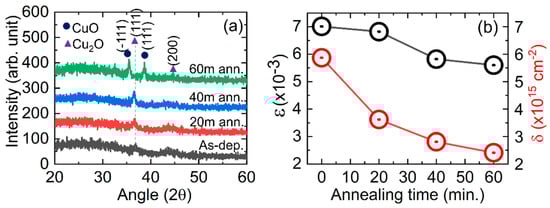
Figure 1.
(a) X-ray Diffraction (XRD) patterns of CuxO thin films prepared in this study and (b) estimated micro-strain (ε) and dislocation density (δ) in the films.

Table 1.
Estimated structural and optical properties of the CuxO thin films with respect to the annealing time.
It should be noted that the very low peak height in all of the films’ XRD patterns, as shown in Table 1, indicates the retention of the amorphous phase in the films. Particularly, the amorphous phase should be reduced with thermal annealing since more energy is supplied for recrystallization and an improvement in the crystallinity of the CuxO thin films; however, no significant change was observed in this study. The recrystallization of the film during thermal annealing may be impacted by N- and/or O-doping; thus, the film crystallinity is unable to be dominant. The average crystallite size of the films was calculated using the Debye–Scherrer formula [28]. From Table 1, it can be seen that the average crystallite size of CuxO is increasing with the increase in annealing time, which is in the range of 16–20 nm. The increase of crystallite size gives an indication of the recrystallization of the film upon thermal annealing. Moreover, the micro-strain () and dislocation density () were also calculated using the formula mentioned in the literature [28], and the findings are shown in Figure 1b. Particularly, ε and δ could be developed in the films via substitution, relocation of the atoms, and/or scattered grain distribution. Hereby, we found that the and for the plane () are reduced in the case of all the thermal-treated films. It may have occurred due to an increase in grain size and grain distribution upon thermal treatment. Also, the reduction of and may have occurred due to the replacement of Cu2+ and O2− atoms in their reference lattice during thermal annealing.
Figure 2a shows the transmittance spectra of as-deposited and thermal-treated CuxO thin films. A clear blue shift, including an increase of average transmittance in the wavelength region (400–900 nm), is seen for the films that underwent 20 min and 40 min of thermal annealing; however, it decreased for films that underwent 60 min of thermal annealing. Additionally, the interference patterns, as observed in the lower wavelength region, indicate the thickness homogeneity and/or surface roughness of the prepared films. Also, this could have occurred due to the difference in the refractive index of the CuxO thin films and substrate and/or the interference of multiple light reflections that occurred during the measurement [29].

Figure 2.
(a) Optical transmittance of the films, (b) bandgap evaluation curves for the CuxO thin films annealed in an N2/O2 (80:20) ambient at different time duration (insets: schematic of bandgap diagrams varied due to the thermal annealing), and (c,d) SEM image for 40 min annealed and 60 min annealed films.
Figure 2b illustrates the estimated values of (αhν)2 plotted against hν to determine the energy bandgap [30]. The estimated bandgap () value ranges from 2.18 eV to 2.34 eV, in good agreement with the other reported study on CuxO thin films [11]. The of the annealed film increased from 2.25 to 2.34 eV when the annealing time increased to 40 min, however, it reduced to 2.18 eV when the annealing time was increased further to 60 min. The decrease in bandgap may be related to the structural transition from Cu2O to CuO, as seen in XRD results. As it is certain that the N- and/or O-doping concentration is depending on the annealing time, we can say that Eg intensely depends on the N- and/or O-doping concentration in the CuxO thin films. A similar phenomenon has also been reported for N-doped Cu2O films [31]. This increase in the optical bandgap of the N-doped Cu2O thin films is also quite similar to the rutile N-doped TiO2 films [32]. It should be noticed that the bandgap widening that occurred due to the N-doping has a limit, whereas it could be saturated in a heavy N-doping range [27]. Thus, the bandgap reduced from 60 min of annealing time. The bandgap widening mechanism is schematically shown for 40 min of annealing in the inset of Figure 2b. Particularly, due to the N-doping, the conduction band edge is negatively shifted and the valance band edge is positively shifted as confirmed by the literature [27]. Figure 2c,d show the surface morphology of CuxO thin films of 20 min and 60 min annealing time. Both films consist entirely of round-shape grains that are aggregated due to their high-surface energy. The average grain size of 20 min annealed film is approximately 12 nm, whereas it is increased to 16 nm from 60 min of annealing time. The increase in grain size may also affect the optical properties that were seen in Figure 2a,b. The change in optical properties and surface morphology reveals the impact of thermal annealing in N2/O2 ambient on the optical properties of CuxO thin films. The films’ refractive index has been measured utilizing the Moss relation [33,34], which is directly related to the fundamental energy bandgap ():
where is a constant of 108 eV. All of the films were tested for both static and high-frequency dielectric constants. The static dielectric constant () was calculated using its relationship with the energy bandgap of the semiconductor compound materials, which could be expressed as [35]:
Also, the high-frequency dielectric constant was estimated from the following relation [34],
For the prepared CuxO films, the estimated , , and values are presented in Table 1. As seen in Table 1, the values of n, , and are slightly decreased until 40 m of annealing; however, they increase significantly from 60 min of annealing. The result is quite consistent with the previous report [36].
Figure 3 shows the PL emission spectra of the CuxO thin film for as-deposited and 40 min annealed films. To determine the accurate peak positions, the peak has been fitted using Gaussian fit. The luminescence at around 600 nm is related to excitons [37], the peak at 630 nm is associated with the direct band-to-band recombination of the phono assisted exciton [38,39], and the peak at around 665 nm is attributed to the recombination of excitons bound to double-charged oxygen vacancies (VO2+) [40]. It has also been reported that the PL emission around 600–630 nm is associated with the direct bandgap of high-quality CuxO thin films [41]. CuO has been reported to have a weak PL signal in the wavelength range of 620–900 nm [42]; thus, the strong peak at around 630 nm found in this study may be represented by Cu2O crystals, which are also supported by the XRD analysis. It can be seen that the exciton luminescence and band-to-band recombination luminescence are higher for the annealed film than as-deposited films, which indicates that the crystalline quality improves after annealing. The peak associated with oxygen vacancies is observed to reduce after thermal annealing for 40 min, which suggests the reduction of oxygen vacancy or increase of oxygen content in the film upon annealing. The increase of oxygen content has also been confirmed by the Energy-dispersive X-ray spectroscopy (EDX) measurement, as shown in Figure 3.
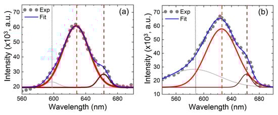
Figure 3.
Photoluminescence spectra of CuxO thin films for as-deposited (a) and annealed (40 min) films (b).
Figure 4a. Moreover, the Full Width at Half Maximum (FWHM) of the fitted peak at around 630 nm for annealed CuxO film is slightly broadened compared with the as-deposited samples. This broadening has been interpreted as a Cu-N bonding [37], which may play an important role in films’ electrical properties.

Figure 4.
(a) The EDX spectra of CuxO thin films (top) as-deposited, (middle) annealed for 40 min, and (bottom) annealed for 60 min and (b) electrical characteristics of the prepared CuxO thin films (color of the legend determine the parameters).
The EDX spectra confirm the presence of copper and oxygen along with other elements from the glass substrates. Cu and O atomic concentrations in as-deposited films were 45.12% and 54.88%, respectively, compared to 37.45% and 62.55% for 40 min annealed films, and 23.82% and 76.18% for 60 min annealed films. The increase in oxygen content in the film confirms the oxygen adsorption into the CuxO lattice. The electrical properties of the CuxO thin films prepared by sputtering and consecutive thermal annealing were investigated using the Hall Effect measurement system, and the results are shown in Figure 4b. Upon thermal annealing, it can be seen that the carrier concentration is slightly increased; however, resistivity is decreased. The lowest (2.71 × 1015 cm−3) and highest (2.83 × 1016 cm−3) carrier concentrations were found for as-deposited and 60 min of thermally annealed film, respectively. It should be noted that the conductivity and carrier concentration in CuxO thin films are directly related to the Cu vacancies in the crystal structure. Particularly, the carriers were generated from the Cu vacancies (acceptor-like) or O vacancies (donor-like) in CuxO films [43]. With close observation, it can be seen that the rise in carrier concentration is minor until 40 min of annealing, but it significantly increases at 60 min of annealing. It has been reported that the Cu vacancies are higher in CuO films than Cu2O films [44,45]. Since upon 60 min of thermal annealing Cu2O is converted to CuO, the highest increment of carrier concentration is observed for 60 min annealed film. On the other hand, it was seen that O content increased in the film of 40 min annealing, but it was only a slight increase of carrier concentration. A possible explanation is that annealing in N2/O2 ambient may also induce the diffusion of nitrogen into film lattice and increase the Cu vacancies. The increase of Cu vacancies as well as hole concentration due to the nitrogen diffusion into the CuxO film has already been reported elsewhere [37]. The variation of annealing time in N2/O2 ambient led to the total variation in Cu or O vacancies, resulting in variation in carrier concentration is observed; however, more study is needed to confirm the impact.
The variations of hole mobility nearly have the opposite trend compared with that of the resistivity. In particular, two factors influenced the films’ resistivity; carrier concentration and mobility (i.e., ). The higher carrier concentration as well as higher mobility yield lower resistivity. The increase of mobility may be related to the improvement of films’ crystal quality, as seen in XRD. In contrast, the mobility decreases for the film annealed for 60 min. It was seen that the CuO phase is dominated in that film, and it was reported that the hole mobility is lower for the CuO film than the corresponding Cu2O film [46]. Particularly, most oxides exhibit poor hole mobility in the valence band because of the localized O 2p states on the upper valence band. The lowest value of mobility 14.18 cm2 V−1 s−1 has been found for the as-deposited film, which improved to as high as 27.51 18 cm2 V−1 s−1 for 40 min of thermally annealed film.
4. Device Simulation
Utilizing the CuxO as a hole transport layer (HTL), the PSC device performance has been investigated using the one-dimensional software SCAPS-1D (version 3.3.01). The optoelectronic properties of CuxO were used as found in this analysis, except that the thickness was set at 80 nm. Readers should refer to the literature for descriptions of SCAPS-1D, including other layer parameters [47]. The energy band diagram of the modeled PSC structure is shown in the inset of Figure 5e. Particularly, the most common HTL for PSCs are organic materials, such as Spiro-OMeTAD, PEDOT: PSS, and Poly[bis(4-phenyl)(2,4,6-trimethylphenyl)amine (PTAA); however, their hygroscopic nature influences the instability of the PSCs [48]. Additionally, various inorganic p-type semiconducting materials as the HTL have been approaches toward the development of highly stable PSCs instead of organic HTLs. Among them, NiOx is one of the most widely investigated HTL because of its high transmittance, large bandgap, deep valence band, and easier deposition technique [49]. Zhang et al. reported the highest PCE to date of 19.47%using NiOx nanocrystal as the HTL in inverted structure PSC [50]. In 2020, Li et al. reported PSC achieving as high as 21.66% PCE via a NiOx/Spiro Bilayers HTL [51]. It should be noted that NiOx-based HTLs show some shortcomings, including low-hole conductivity and poor electrical and/or physical contact with the perovskite layer. On the other hand, CuxO material as an HTL has superior properties, including deep valence band and high carrier mobility. The only drawback is its low optical bandgap, which brought significant optical losses, thus widening the optical bandgap of CuxO thin film, considering a crucial scope that could be achieved via appropriate doping and/or modifying the fabrication technique. The PSC using Cr-doped CuxO HTL already showed high-conversion efficiencies of 20.54% and significantly improved the cell stability [49]. Figure 5 and Table 2 shows the results found from the numerical simulation utilizing the inverted planner PSC structure of Glass/FTO/CuxO/MAIPbI3/PCBM/Ag.
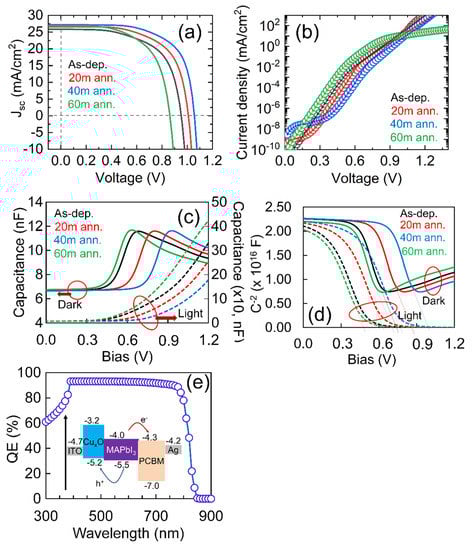
Figure 5.
(a) The light current density-voltage (J-V) curves, (b) Semi-log plot of dark current-voltage (I-V) curve found for PSCs with different CuxO thin films, (c,d) shows the capacitance-voltage curves in light and dark mode for the modeled PSCs and (e) shows the external quantum efficiency (EQE) for the highest-efficiency PSC using 40 m annealed CuxO thin film (inset shows the schematic band diagram of the PSC used in this study).
Table 2.
The performance parameter, including electrical properties of the perovskite solar cells, using CuxO thin films as a hole transport material (HTM).
Figure 5a,b and Table 2 show the light and dark current-voltage characteristics of the simulated PSCs using different optical and electrical properties of the CuxO thin films found in this study. It could be seen that all the performance parameters are improved until 40 min of thermal annealing, which reduced the further increase of annealing time to 60 min. It could be seen that Voc and Jsc varied significantly, as similar to fill factor (FF). It is well-known that FF is directly related to the charge extraction and transport that occurred in PSC. Further, the extraction and transport of charges depend on the mobility of the carrier, the morphology of the film, and the interfacial and bulk charge recombination rates of the solar cell. Also, in the case of the conventional p-i-n semiconductor model, Voc relies on the splitting of the quasi-Fermi energy levels of the electron and hole in the entire system, and Jsc is determined by the carrier recombination that may influence by the interface states as well as defects in the individual active layers. Also, the spectral response of the perovskite materials influences Jsc. Thus, the PSC’s performance is significantly affected by the charge transport layer and energy distribution of the perovskite thin films [52,53]. To understand the variation of the performance parameters better, the semi-log plot of the dark IV of PSCs with different CuxO thin films was investigated, as shown in Figure 5b. The minimum ideality factor (n) and dark recombination current (Io) are found for the CuxO film that had been annealed for 40 min. From the previous section’s results, it could be predicted that optimum N-doping occurs when the film is annealed for 40 min, resulting in the highest bandgap, which confirms the lowest optical loss, highest hole mobility, and highest carrier concentration that may influence the n and Io to reduce. The lowest value of n and Io lead to the highest device efficiency, as seen in Table 2. Also, we use capacitance-voltage (CV) measurements in both dark and illumination conditions to evaluate the impact of CuxO materials on the built-in potential (Vbi) of PSCs. Based on the CV characteristics shown in Figure 5c,d, the Vbi is estimated by the intercept according to the classic Mott–Schottky model [54,55]. As shown in Figure 5d, the Vbi of the PSCs with different CuxO HTLs fabricated in this study are determined to be 0.72 V and 1.0 V in dark conditions and 0.53 V to 0.75 V under light (one-sun) condition, respectively. The impact of the optical and electrical properties of the CuxO materials on the device Vbi in both dark and illumination conditions is seen here. Particularly, the Vbi is determined by the bulk band offset in solar cells and the energy difference between the interfaces of different layers. In the case of PSCs, the Vbi is determined by the energy difference at the interface of cathode/ETL and anode/HTL and the bulk polarization from the grain boundary defects [56]. Moreover, in the case of the passivated grain boundary, the Vbi is then mostly controlled by the energy difference at the interface of cathode/ETL and anode/HTL in PSCs, such as a metal-insulator-metal (MIM) model. This implies that the properties of the transport layer have a major effect on the Vbi of PSCs, as seen in this study.
Additionally, cathode/ETL and the anode/HTL interfaces could contribute to the photoexcitation because of the accumulation of photo-generated carriers at their interfaces. Consequently, the Vbi could be divided into static and dynamic components defined by the energy difference at the interface of cathode/ETL and anode/HTL and the accumulation of photo-generated carriers at their interface. Particularly, the Vbi is mainly affected by the dynamic component, namely the accumulation of photo-generated carriers at their interface [57,58]. In this study, the Vpeak shift with the increase of annealing time until 40 min, as seen in Figure 5c, reflects the interfacial photo-generated carrier accumulation in solar cells [58]. Also, the height of the Vpeak reflects the density of the accumulated photo-generated carriers at the interface. This suggests a reduced interface-charge accumulation occurred for the CuxO film of 40 min annealed, which forms higher Vbi through a dynamic parameter in the PSC. Figure 5e shows the external quantum efficiency (EQE) for the highest-achieved efficiency for the CuxO HTL prepared by 40 min of thermal annealing in N2/O2 ambient. The best efficiency achieved in this study is 19.70% with a Voc of 1.06 V, a Jsc of 27.14 mA/cm2, and a fill factor (FF) of 68.65%. The PSC’s efficiency is shown to be highly dependent on the properties of CuxO thin films, meaning that CuxO HTL needs much more research to obtain the most effective and stable PSCs. According to the results found in this study, CuxO thin film could certainly be a better potential HTL than other materials currently used in PSCs.
5. Conclusions
In our work, the properties of reactive-sputtered CuxO thin films have been demonstrated elaborately using XRD, SEM, EDX, UV-Vis, PL, and Hall effect measurement techniques. The film’s structural and optical properties were found to be dependent on the subsequent air annealing time, as well as the amount of oxygen that was incorporated during the annealing process. The CuxO film’s crystal properties were found to improve until 40 min of annealing; however, the film annealed for 60 min showed dominant CuO crystal. The optical bandgap has been found to increase until 40 min of annealing, and the decrease in further increase of annealing time to 60 min may be due to the major crystallographic change, as seen in XRD. Films’ refractive index and dielectric constants also varied similar to the optical bandgap. The PL deconvolution showed that the exciton-assisted band-to-band recombination is increased upon thermal annealing. The hole mobility is observed to increase until 40 min of annealing time, and resistivity is oppositely varied. The highest hole mobility (27.51 cm2 V−1 s−1) has been achieved in this study. Form the numerical simulation, the minimum ideality factor (n) and the dark recombination current (Io) in PSC were found for the CuxO film that had been annealed for 40 min. The C-V analysis showed that CuxO films have better energy level alignment with perovskite film and the low interface-charge accumulation, and a higher Vbi has been found for 40 min annealed film. According to the simulation results, a 40 min annealed CuxO film showed the highest efficiency of 22.56% with performance parameters, Voc = 1.06 V, Jsc = 27.14 mA/cm2, and FF = 78.65%. The improved photovoltaic performance implies that CuxO is a promising HTM for future efficient and stable low-temperature roll-to-roll perovskite solar cell fabrication.
Author Contributions
The experiments were planned and carried out by M.A.I. and Y.A.W.; M.A.I. led the manuscript writing effort, with support from M.U.K. and D.A.B.; M.U.K., A.A., and A.S.A.A. contributed to the interpretation of the results and helped to carry out the experiments. N.A. has supervised the research. The findings were discussed by all contributors, and they all contributed to the final manuscript. All authors have read and agreed to the published version of the manuscript.
Funding
This work was supported by the Malaysian Ministry of Higher Education through the FRGS grant FRGS/1/2020/TK0/UM/02/33 and the Taif University for partial support through the Project number (TURSP-2020/163), Taif 21944, Saudi Arabia.
Data Availability Statement
Data is contained within the article.
Acknowledgments
The authors also acknowledge the support from the Faculty of Engineering, Universiti Malaya (@UM) for other support.
Conflicts of Interest
The authors declare no conflict of interest.
References
- Qidong, T.; Tang, K.-C.; Yan, F. Recent Progress of Inorganic Perovskite Solar Cells. Energy Environ. Sci. 2019, 12, 2375–2405. [Google Scholar]
- Ibn-Mohammed, T.; Koh, S.C.L.; Reaney, I.M.; Acquaye, A.; Schileo, G.; Mustapha, K.B.; Greenough, R. Perovskite Solar Cells: An Integrated Hybrid Lifecycle Assessment and Review in Comparison with Other Photovoltaic Technologies. Renew. Sustain. Energy Rev. 2017, 80, 1321–1344. [Google Scholar] [CrossRef]
- Ball, J.M.; Stranks, S.D.; Hörantner, M.T.; Hüttner, S.; Zhang, W.; Crossland, E.J.W.; Ramirez, I.; Moritz, R.; Johnston, M.B.; Friend, R.H.; et al. Optical Properties and Limiting Photocurrent of Thin-Film Perovskite Solar Cells. Energy Environ. Sci. 2015, 8, 602–609. [Google Scholar] [CrossRef]
- Zhou, D.; Zhou, T.; Yu, T.; Zhu, X.; Tu, Y. Perovskite-Based Solar Cells: Materials, Methods, and Future Perspectives. J. Nanomater. 2018, 2018, 8148072. [Google Scholar] [CrossRef]
- Bhat, A.; Dhamaniya, B.P.; Chhillar, P.; Korukonda, T.B.; Rawat, G.; Pathak, S.K. Analysing the Prospects of Perovskite Solar Cells within the Purview of Recent Scientific Advancements. Crystals 2018, 8, 242. [Google Scholar] [CrossRef]
- Chen, L.X. Beyond PCE: Looking at a Big Picture in Photovoltaic Research. ACS Energy Lett. 2018, 3, 1967–1968. [Google Scholar] [CrossRef]
- Malinkiewicz, O.; Yella, A.; Lee, Y.H.; Espallargas, G.M.; Graetzel, M.; Nazeeruddin, M.K.; Bolink, H.J. Perovskite Solar Cells Employing Organic Charge-Transport Layers. Nat. Photonics 2014, 8, 128–132. [Google Scholar] [CrossRef]
- Zhu, Z.; Bai, Y.; Zhang, T.; Liu, Z.; Long, X.; Wei, Z.; Wang, Z.; Zhang, L.; Wang, J.; Yan, F.; et al. High-Performance Hole-Extraction Layer of Sol–Gel-Processed NiO Nanocrystals for Inverted Planar Perovskite Solar Cells. Angew. Chem. 2014, 126, 12779–12783. [Google Scholar] [CrossRef]
- Rong, Y.; Hu, Y.; Mei, A.; Tan, H.; Saidaminov, M.I.; Il Seok, S.; McGehee, M.D.; Sargent, E.H.; Han, H. Challenges for Commercializing Perovskite Solar Cells. Science 2018, 361, 6408. [Google Scholar] [CrossRef]
- Ito, S.; Tanaka, S.; Manabe, K.; Nishino, H. Effects of Surface Blocking Layer of Sb2S3 on Nanocrystalline TiO2 for CH3NH3PbI3 Perovskite Solar Cells. J. Phys. Chem. C 2014, 118, 16995–17000. [Google Scholar] [CrossRef]
- Wang, K.C.; Jeng, J.Y.; Shen, P.S.; Chang, Y.C.; Diau, E.W.G.; Tsai, C.H.; Chao, T.Y.; Hsu, H.C.; Lin, P.Y.; Chen, P.; et al. P-Type Mesoscopic Nickel Oxide/Organometallic Perovskite Heterojunction Solar Cells. Sci. Rep. 2014, 4, 1–8. [Google Scholar] [CrossRef] [PubMed]
- Ye, S.; Sun, W.; Li, Y.; Yan, W.; Peng, H.; Bian, Z.; Liu, Z.; Huang, C. CuSCN-Based Inverted Planar Perovskite Solar Cell with an Average PCE of 15.6%. Nano Lett. 2015, 15, 3723–3728. [Google Scholar] [CrossRef] [PubMed]
- Jeffrey, A.C.; Fung, R.C.M.; Kamat, P.V. An Inorganic Hole Conductor for Organo-Lead Halide Perovskite Solar Cells. Improved Hole Conductivity with Copper Iodide. J. Am. Chem. Soc. 2014, 136, 758–764. [Google Scholar]
- Wu, Z.; Bai, S.; Xiang, J.; Yuan, Z.; Yang, Y.; Cui, W.; Gao, X.; Liu, Z.; Jin, Y.; Sun, B. Efficient Planar Heterojunction Perovskite Solar Cells Employing Graphene Oxide as Hole Conductor. Nanoscale 2014, 6, 10505–10510. [Google Scholar] [CrossRef]
- Zuo, C.; Ding, L. Solution-Processed Cu2O and CuO as Hole Transport Materials for Efficient Perovskite Solar Cells. Small 2015, 11, 5528–5532. [Google Scholar] [CrossRef]
- Jiang, T.; Xie, T.; Zhang, Y.; Chen, L.; Peng, L.; Li, H.; Wang, D. Photoinduced Charge Transfer in ZnO/Cu2O Heterostructure Films Studied by Surface Photovoltage Technique. Phys. Chem. Chem. Phys. 2010, 12, 15476–15481. [Google Scholar] [CrossRef]
- Chatterjee, S.; Pal, A.J. Introducing Cu2O Thin Films as a Hole-Transport Layer in Efficient Planar Perovskite Solar Cell Structures. J. Phys. Chem. C 2016, 120, 1428–1437. [Google Scholar] [CrossRef]
- Joseph, S.; Kamath, P.V. Electrochemical Deposition of Cu2O on Stainless Steel Substrates: Promotion and Suppression of Oriented Crystallization. Solid State Sci. 2008, 10, 1215–1221. [Google Scholar] [CrossRef]
- Fujiwara, T.; Nakaue, T.; Yoshimura, M. Direct Fabrication and Patterning of Cu2O Film by Local Electrodeposition Method. Solid State Ion. 2004, 175, 541–544. [Google Scholar] [CrossRef]
- Chen, L.C.; Wang, C.C.; Lu, S.W. Annealing Effects of Sputtered Cu2O Nanocolumns on ZnO-Coated Glass Substrate for Solar Cell Applications. J. Nanomater. 2013, 2013, 891365. [Google Scholar] [CrossRef]
- Jimenez-Cadena, G.; Comini, E.; Ferroni, M.; Sberveglieri, G. Synthesis of Cu2O Bi-Pyramids by Reduction of Cu(OH)2 in Solution. Mater. Lett. 2010, 64, 469–471. [Google Scholar] [CrossRef]
- Nordseth, Ø.; Kumar, R.; Bergum, K.; Chilibon, I.; Foss, S.E.; Monakhov, E. Nitrogen-Doped Cu2O Thin Films for Photovoltaic Applications. Materials 2019, 12, 3038. [Google Scholar] [CrossRef]
- Sun, W.; Li, Y.; Ye, S.; Rao, H.; Yan, W.; Peng, H.; Li, Y.; Liu, Z.; Wang, S.; Chen, Z.; et al. High-Performance Inverted Planar Heterojunction Perovskite Solar Cells Based on a Solution-Processed CuO x Hole Transport Layer. Nanoscale 2016, 8, 10806–10813. [Google Scholar] [CrossRef]
- Dubale, A.A.; Pan, C.J.; Tamirat, A.G.; Chen, H.M.; Su, W.N.; Chen, C.H.; Rick, J.; Ayele, D.W.; Aragaw, B.A.; Lee, J.F.; et al. Heterostructured Cu2O/CuO Decorated with Nickel as a Highly Efficient Photocathode for Photoelectrochemical Water Reduction. J. Mater. Chem. A 2015, 3, 12482–12499. [Google Scholar] [CrossRef]
- Murali, D.S.; Kumar, S.; Choudhary, R.J.; Wadikar, A.D.; Jain, M.K.; Subrahmanyam, A. Synthesis of Cu2O from CuO Thin Films: Optical and Electrical Properties. AIP Adv. 2015, 5, 047143. [Google Scholar] [CrossRef]
- Gupta, D.; Meher, S.R.; Illyaskutty, N.; Alex, Z.C. Facile Synthesis of Cu2O and CuO Nanoparticles and Study of Their Structural, Optical and Electronic Properties. J. Alloys Compd. 2018, 743, 737–745. [Google Scholar] [CrossRef]
- Nakano, Y.; Saeki, S.; Morikawa, T. Optical Bandgap Widening of p-type Cu2O Films by Nitrogen Doping. Appl. Phys. Lett. 2009, 94, 022111. [Google Scholar] [CrossRef]
- Islam, M.A.; Rahman, K.S.; Misran, H.; Asim, N.; Hossain, M.S.; Akhtaruzzaman, M.; Amin, N. High Mobility and Transparent ZTO ETM Prepared by RF Reactive Co-Sputtering for Perovskite Solar Cell Application. Results Phys. 2019, 14, 102518. [Google Scholar] [CrossRef]
- Moshfegh, A.Z.; Azimirad, R.; Akhavan, O. Optical Properties and Surface Morphology of Evaporated (WO3)1− x–(Fe2O3)x Thin Films. Thin Solid Film. 2005, 484, 124–131. [Google Scholar] [CrossRef]
- Islam, M.A.; Misran, H.; Akhtaruzzaman, M.; Amin, N. Influence of Oxygen on Structural and Optoelectronic Properties of CdS Thin Film Deposited by Magnetron Sputtering Technique. Chin. J. Phys. 2020, 67, 170–179. [Google Scholar] [CrossRef]
- Ishizuka, S.; Suzuki, K.; Okamoto, Y.; Yanagita, M.; Sakurai, T.; Akimoto, K.; Fujiwara, N.; Kobayashi, H.; Matsubara, K.; Niki, S. Polycrystalline n-ZnO/p-Cu2O Heterojunctions Grown by RF-Magnetron Sputtering. Phys. Status Solidi (c) 2004, 1, 1067–1070. [Google Scholar] [CrossRef]
- Diwald, O.; Thompson, T.L.; Zubkov, T.; Goralski, E.G.; Walck, S.D.; Yates, J.T. Photochemical Activity of Nitrogen-Doped Rutile TiO2 (110) in Visible Light. J. Phys. Chem. B 2004, 108, 6004–6008. [Google Scholar] [CrossRef]
- Akaltun, Y.; Yıldırım, M.A.; Ateş, A.; Yıldırım, M. Zinc Concentration Effect on Structural, Optical and Electrical Properties of Cd1− xZnxSe Thin Films. Mater. Res. Bull. 2012, 47, 3390–3396. [Google Scholar] [CrossRef]
- Hannachi, L.; Bouarissa, N. Band Parameters for Cadmium and Zinc Chalcogenide Compounds. Phys. B Condens. Matter 2009, 404, 3650–3654. [Google Scholar] [CrossRef]
- Mezrag, F.; Mohamed, W.K.; Bouarissa, N. The Effect of Zinc Concentration upon Optical and Dielectric Properties of Cd1− xZnxSe. Phys. B Condens. Matter 2010, 405, 2272–2276. [Google Scholar] [CrossRef]
- Akaltun, Y. Effect of Thickness on the Structural and Optical Properties of CuO Thin Films Grown by Successive Ionic Layer Adsorption and Reaction. Thin Solid Film. 2015, 594, 30–34. [Google Scholar] [CrossRef]
- Li, J.; Mei, Z.; Liu, L.; Liang, H.; Azarov, A.; Kuznetsov, A.; Liu, Y.; Ji, A.; Meng, Q.; Du, X. Probing Defects in Nitrogen-Doped Cu2O. Sci. Rep. 2014, 4, 1–6. [Google Scholar]
- Izaki, M.; Sasaki, S.; Mohamad, F.B.; Shinagawa, T.; Ohta, T.; Watase, S.; Sasano, J. Effects of Preparation Temperature on Optical and Electrical Characteristics of (111)-Oriented Cu2O Films Electrodeposited on (111)-Au Film. Thin Solid Film. 2012, 520, 1779–1783. [Google Scholar] [CrossRef]
- Liu, Y.L.; Liu, Y.C.; Mu, R.; Yang, H.; Shao, C.L.; Zhang, J.Y.; Lu, Y.M.; Shen, D.Z.; Fan, X.W. The Structural and Optical Properties of Cu2O Films Electrodeposited on Different Substrates. Semicond. Sci. Technol. 2004, 20, 44. [Google Scholar] [CrossRef]
- Yu, W.L.; Lin, Y.Z.; Zhu, X.W.; Hu, Z.G.; Han, M.J.; Cai, S.S.; Chen, L.L.; Shao, H.H. Diversity of Electronic Transitions and Photoluminescence Properties of p-type Cuprous Oxide Films: A Temperature-Dependent Spectral Transmittance Study. J. Appl. Phys. 2015, 117, 045701. [Google Scholar]
- Gan, J.; Galeckas, A.; Venkatachalapathy, V.; Riise, H.N.; Svensson, B.G.; Monakhov, E.V. Study of Photoluminescence Properties of CuxO Thin Films Prepared by Reactive Radio Frequency Magnetron Sputtering. MRS Online Proc. Libr. 2015, 1792, 1–7. [Google Scholar] [CrossRef]
- Huang, C.Y.; Chatterjee, A.; Liu, S.B.; Wu, S.Y.; Cheng, C.L. Photoluminescence Properties of a Single Tapered CuO Nanowire. Appl. Surf. Sci. 2010, 256, 3688–3692. [Google Scholar] [CrossRef]
- Jeong, Y.K.; Choi, G.M. Nonstoichiometry and Electrical Conduction of CuO. J. Phys. Chem. Solids 1996, 57, 81–84. [Google Scholar] [CrossRef]
- Wu, D.; Zhang, Q.; Tao, M. LSDA+ U Study of Cupric Oxide: Electronic Structure and Native Point Defects. Phys. Rev. B 2006, 73, 235206. [Google Scholar] [CrossRef]
- Hu, X.; Gao, F.; Xiang, Y.; Wu, H.; Zheng, X.; Jiang, J.; Li, J.; Yang, H.; Liu, S. Influence of Oxygen Pressure on the Structural and Electrical Properties of CuO Thin Films Prepared by Pulsed Laser Deposition. Mater. Lett. 2016, 176, 282–284. [Google Scholar] [CrossRef]
- Yao, Z.Q.; Liu, S.L.; Zhang, L.; He, B.; Kumar, A.; Jiang, X.; Zhang, W.J.; Shao, G. Room Temperature Fabrication of p-channel Cu2O Thin-Film Transistors on Flexible Polyethylene Terephthalate Substrates. Appl. Phys. Lett. 2012, 101, 042114. [Google Scholar] [CrossRef]
- Hajjiah, A.; Kandas, I.; Shehata, N. Efficiency Enhancement of Perovskite Solar Cells with Plasmonic Nanoparticles: A Simulation Study. Materials 2018, 11, 1626. [Google Scholar] [CrossRef] [PubMed]
- Pitchaiya, S.; Natarajan, M.; Santhanam, A.; Asokan, V.; Yuvapragasam, A.; Ramakrishnan, V.M.; Palanisamy, S.E.; Sundaram, S.; Velauthapillai, D. A Review on the Classification of Organic/Inorganic/Carbonaceous Hole Transporting Materials for Perovskite Solar Cell Application. Arab. J. Chem. 2020, 13, 2526–2557. [Google Scholar] [CrossRef]
- Kung, P.K.; Li, M.H.; Lin, P.Y.; Chiang, Y.H.; Chan, C.R.; Guo, T.F.; Chen, P. A Review of Inorganic Hole Transport Materials for Perovskite Solar Cells. Adv. Mater. Interfaces 2018, 5, 1800882. [Google Scholar] [CrossRef]
- Zhang, W.; Song, J.; Wang, D.; Deng, K.; Wu, J.; Zhang, L. Dual Interfacial Modification Engineering with p-type NiO NanoCrystals for Preparing Efficient Planar Perovskite Solar Cells. J. Mater. Chem. C 2018, 6, 13034–13042. [Google Scholar] [CrossRef]
- Li, R.; Wang, P.; Chen, B.; Cui, X.; Ding, Y.; Li, Y.; Zhang, D.; Zhao, Y.; Zhang, X. NiOx/Spiro Hole Transport Bilayers for Stable Perovskite Solar Cells with Efficiency Exceeding 21%. ACS Energy Lett 2019, 5, 79–86. [Google Scholar] [CrossRef]
- Edri, E.; Kirmayer, S.; Henning, A.; Mukhopadhyay, S.; Gartsman, K.; Rosenwaks, Y.; Hodes, G.; Cahen, D. Why Lead Methylammonium Tri-Iodide Perovskite-Based Solar Cells Require a Mesoporous Electron Transporting Sscaffold (But Not Necessarily a Hole Conductor). Nano Lett. 2014, 14, 1000–1004. [Google Scholar] [CrossRef]
- Shao, Y.; Yuan, Y.; Huang, J. Correlation of Energy Disorder and Open-Circuit Voltage in Hybrid Perovskite Solar Cells. Nat. Energy 2016, 1, 1–6. [Google Scholar] [CrossRef]
- Perrier, G.; De Bettignies, R.; Berson, S.; Lemaître, N.; Guillerez, S. Impedance Spectrometry of Optimized Standard and Inverted P3HT-PCBM Organic Solar Cells. Sol. Energy Mater. Sol. Cells 2012, 101, 210–216. [Google Scholar] [CrossRef]
- Fabregat-Santiago, F.; Garcia-Belmonte, G.; Bisquert, J.; Bogdanoff, P.; Zaban, A. Mott-Schottky Analysis of Nanoporous Semiconductor Electrodes in Dielectric State Deposited on SnO2 (F) Conducting Substrates. J. Electrochem. Soc. 2003, 150, E293. [Google Scholar] [CrossRef]
- Lin, P.Y.; Wu, T.; Ahmadi, M.; Liu, L.; Haacke, S.; Guo, T.F.; Hu, B. Simultaneously Enhancing Dissociation and Suppressing Recombination in Perovskite Solar Cells. Nano Energy 2017, 36, 95–101. [Google Scholar] [CrossRef]
- Wu, T.; Hsiao, Y.C.; Li, M.; Kang, N.G.; Mays, J.W.; Hu, B. Dynamic Coupling Between Electrode Interface and Donor/Acceptor Interface via Charge Dissociation in Organic Solar Cells at Device-Operating Condition. J. Phys. Chem. C 2015, 119, 2727–2732. [Google Scholar] [CrossRef]
- Luo, D.; Chen, Q.; Qiu, Y.; Zhang, M.; Liu, B. Device Engineering for All-Inorganic Perovskite Light-Emitting Diodes. Nanomaterials 2019, 9, 1007. [Google Scholar] [CrossRef]
Publisher’s Note: MDPI stays neutral with regard to jurisdictional claims in published maps and institutional affiliations. |
© 2021 by the authors. Licensee MDPI, Basel, Switzerland. This article is an open access article distributed under the terms and conditions of the Creative Commons Attribution (CC BY) license (https://creativecommons.org/licenses/by/4.0/).