Investigation of 1/f and Lorentzian Noise in TMAH-treated Normally-Off GaN MISFETs


Abstract
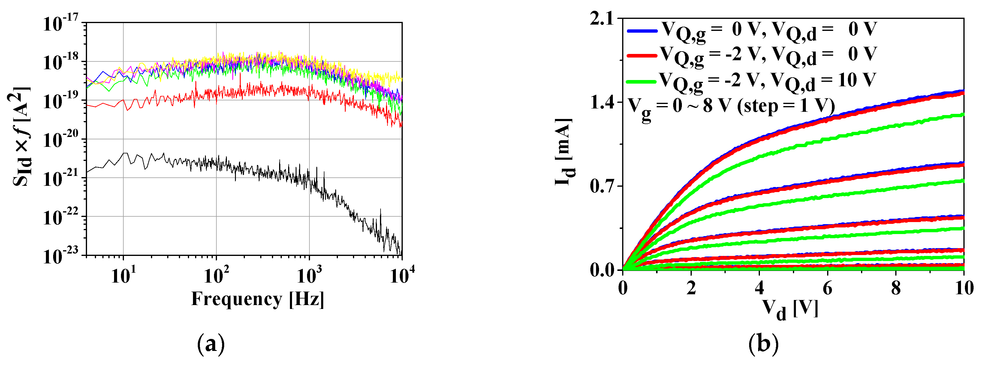
:
1. Introduction
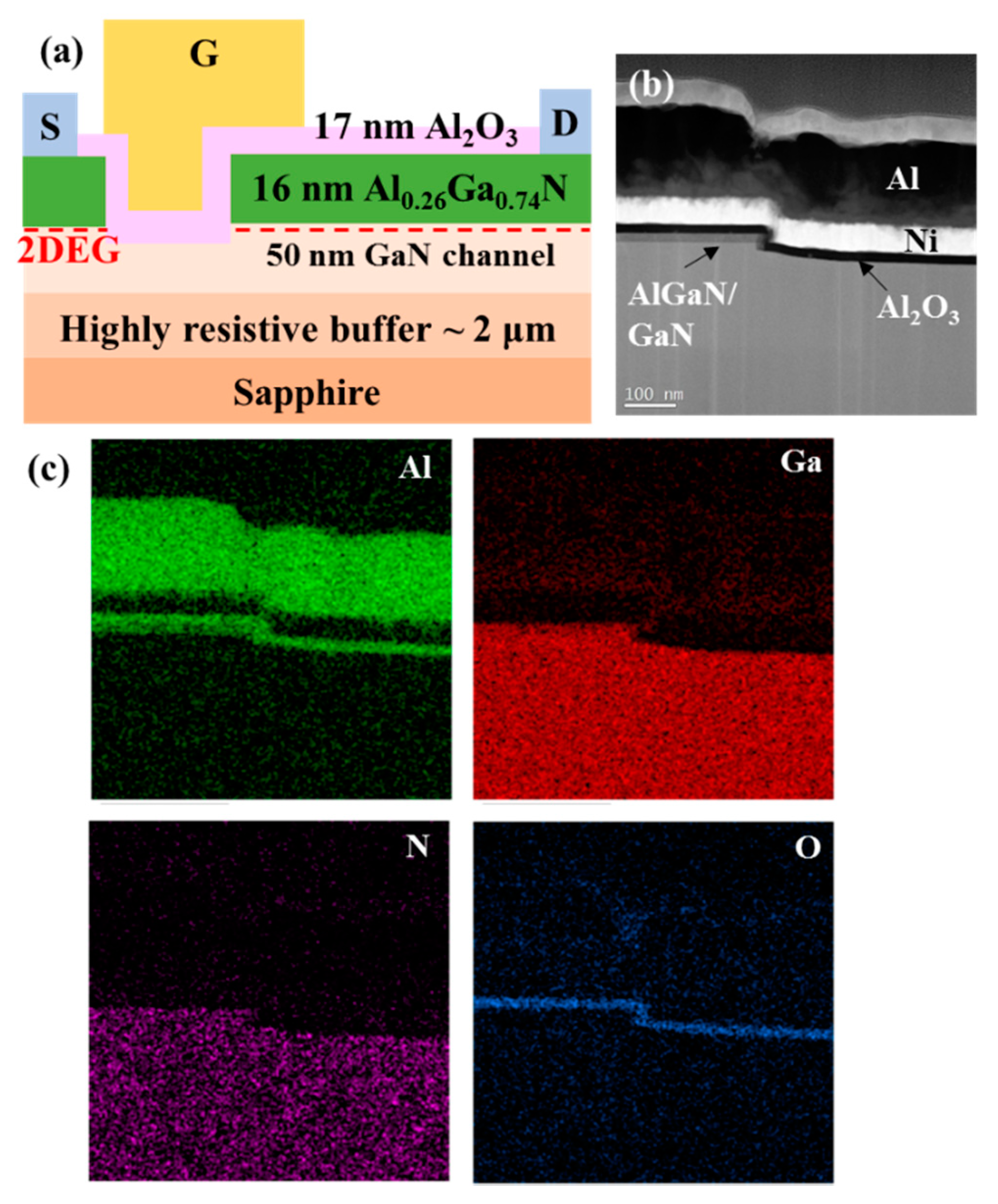
2. Materials and Methods
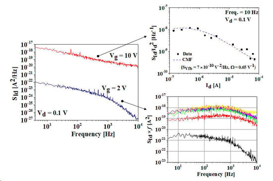
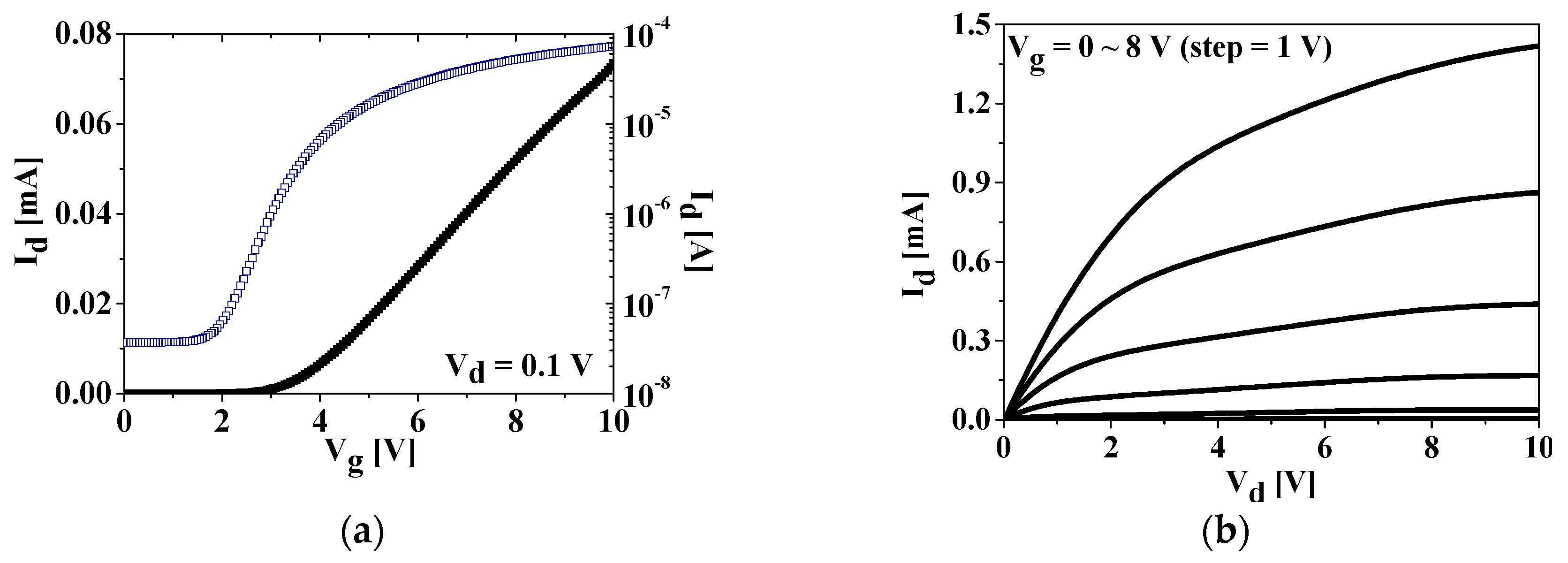
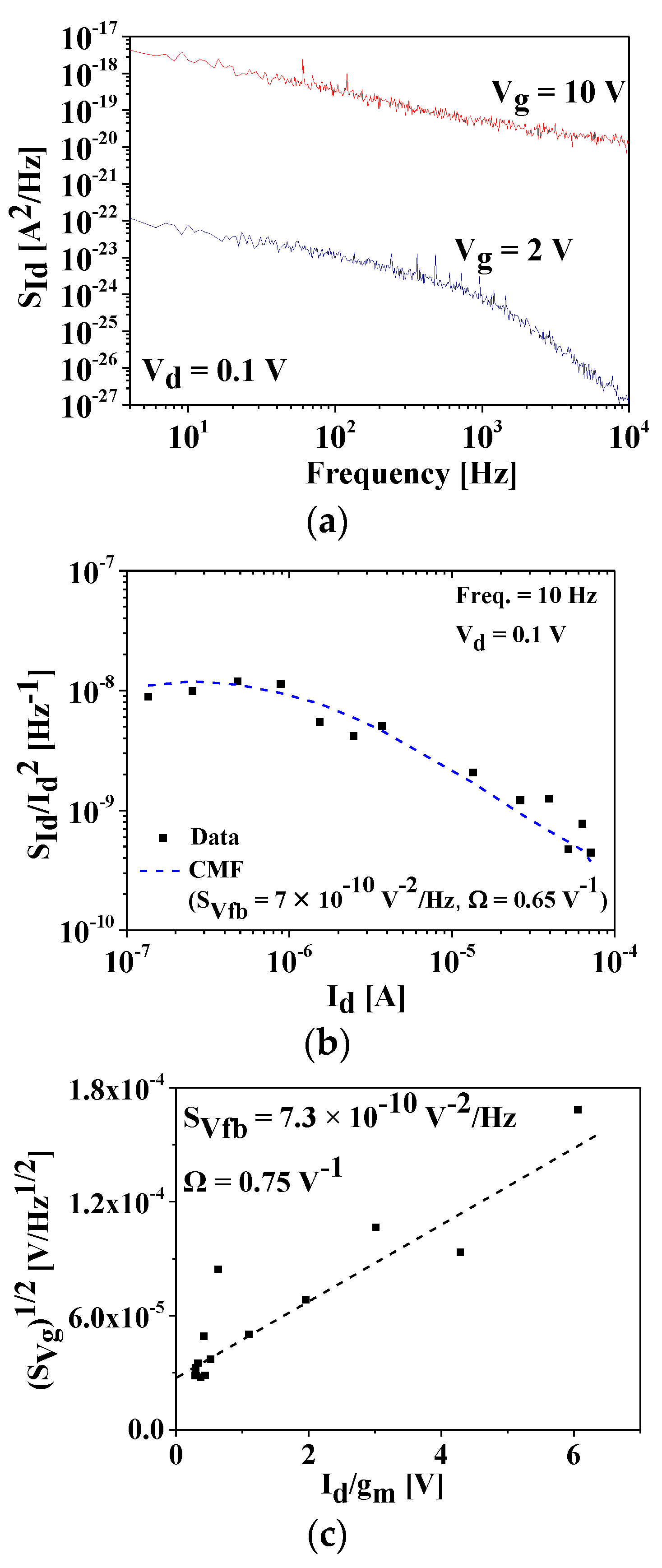
3. Results and Discussion
4. Conclusions
Author Contributions
Funding
Conflicts of Interest
References
- Im, K.-S.; Ha, J.-B.; Kim, K.-W.; Lee, J.-S.; Kim, D.-S.; Hahm, S.-H.; Lee, J.-H. Normally Off GaN MOSFET Based on AlGaN/GaN Heterostructure with Extremely High 2DEG Density Grown on Silicon Substrate. IEEE Electron Device Lett. 2010, 31, 192–194. [Google Scholar]
- Kim, K.-W.; Jung, S.-D.; Kim, D.-S.; Kang, H.-S.; Im, K.-S.; Oh, J.-J.; Ha, J.-B.; Shin, J.-K.; Lee, J.-H. Effects of TMAH Treatment on Device Performance of Normally Off Al2O3/GaN MOSFET. IEEE Electron Device Lett. 2011, 32, 1376–1378. [Google Scholar] [CrossRef]
- Sakong, S.; Lee, S.-H.; Rim, T.; Jo, Y.-W.; Lee, J.-H.; Jeong, Y.-H. 1/f Noise Characteristics of Surface-Treated Normally-Off Al2O3/GaN MOSFETs. IEEE Electron Device Lett. 2015, 36, 229–231. [Google Scholar] [CrossRef]
- Yin, R.; Li, Y.; Sun, Y.; Wen, C.P.; Hao, Y.; Wang, M. Correlation between border traps and exposed surface properties in gate recessed normally-off Al2O3/GaN MOSFET. Appl. Phys. Lett. 2018, 112, 233505. [Google Scholar] [CrossRef]
- Choi, H.-S. Mobility Degradation Effect to Hooge’s Constant in Recessed-Gate Al2O3/AlGaN/GaN MIS Power Transistors. IEEE Electron Device Lett. 2014, 35, 624–626. [Google Scholar]
- Sindhuri, V.; Son, D.-H.; Lee, D.-G.; Sakong, S.; Jeong, Y.-H.; Cho, I.-T.; Lee, J.-H.; Kim, Y.-T.; Cristoloveanu, S.; Bae, Y.; et al. 1/f Noise Characteristics of AlGaN/GaN FinFETs with and without TMAH surface treatment. Microelectron. Eng. 2015, 147, 134–136. [Google Scholar] [CrossRef]
- Reddy, M.S.P.; Lee, J.-H.; Jang, J.-S. Electrical Characteristics of TMAH-Surface Treated Ni/Au/Al2O3/GaN MIS Schottky Structures. Electron. Mater. Lett. 2014, 10, 411–416. [Google Scholar] [CrossRef]
- Reddy, M.S.P.; Park, H.; Kim, S.-M.; Jang, S.-H.; Jang, J.-S. High-performance light-emitting diodes using hierarchically mplane GaN nano-prism light extractors. J. Mater. Chem. C 2015, 3, 8873–8880. [Google Scholar]
- Reddy, M.S.P.; Son, D.-H.; Lee, J.-H.; Jang, J.-S.; Reddy, V.R. Influence of tetramethylammonium hydroxide treatment on the electrical characteristics of Ni/Au/GaN Schottky barrier diode. Mater. Chem. Phys. 2014, 143, 801–805. [Google Scholar] [CrossRef]
- Im, K.-S.; Choi, J.S.; Hwang, Y.M.; An, S.J.; Roh, J.-S.; Kang, S.-H.; Lee, J.-H.; Lee, J.-H. 1/f Noise Characteristics of AlGaN/GaN HEMTs with Periodically Carbon-doped GaN Buffer Layer. Microelectron. Eng. 2019, 215, 110985. [Google Scholar] [CrossRef]
- Reddy, M.S.P.; Caulmilone, R.; Cristoloveanu, S.; Im, K.-S.; Lee, J.-H. Trap and 1/f-noise effects at the surface and core of GaN nanowire gate-all-around FET structure. Nano Res. 2019, 12, 809–814. [Google Scholar] [CrossRef]
- Im, K.-S.; An, S.J.; Theodorou, C.G.; Ghibaudo, G.; Cristoloveanu, S.; Lee, J.-H. Effect of Gate Structure on the Trapping Behavior of GaN Junctionless FinFETs. IEEE Electron Device Lett. 2020, 41, 832–835. [Google Scholar] [CrossRef]
- He, Z.; Chen, Y.; He, J.; Su, W.; Fang, W.; En, Y.; Huang, Y.; Liu, Y. Hydrogen effects on AlGaN/GaN MISFET with LPCVD-SiNx gate dielectric. Semicond. Sci. Technol. 2019, 34, 035020. [Google Scholar] [CrossRef]
- Chen, Y.Q.; Zhang, Y.C.; Liu, Y.; Liao, X.Y.; En, Y.F.; Fang, W.X.; Huang, Y. Effect of Hydrogen on Defects of AlGaN/GaN HEMTs Characterized by Low-Frequency Noise. IEEE Trans. Electron Devices 2018, 65, 1321–1326. [Google Scholar] [CrossRef]
- McWhorter, A.L. 1/f Noise and Germanium Surface Properties in Semiconductor Surface Physics; University of Pennsylvania Press: Philadelphia, PA, USA, 1957; pp. 207–208. [Google Scholar]
- Vandamme, L.K.J.; Hooge, F.N. What do we certainly know about1/f noise in MOSTs? IEEE Trans. Electron. Devices 2008, 55, 3070–3085. [Google Scholar] [CrossRef]
- Ohba, Y.; Hatano, A. A study on strong memory effects for Mg doping in GaN metalorganic chemical vapor deposition. J. Cryst. Growth 1994, 145, 214–218. [Google Scholar] [CrossRef]
- Heikman, S.; Keller, S.; DenBaars, S.P.; Mishra, U.K. Growth of Fe doped semi-insulating GaN by metalorganic chemical vapor deposition. Appl. Phys. Lett. 2002, 81, 439–441. [Google Scholar] [CrossRef]
- Kang, H.-S.; Won, C.-H.; Kim, Y.-J.; Kim, D.-S.; Yoon, Y.J.; Kang, I.M.; Lee, Y.S.; Lee, J.-H. Suppression of current collapse in AlGaN/GaN MISHFET with carbondoped GaN/undoped GaN multilayered buffer structure. Phys. Status Solidi A 2015, 212, 1116–1121. [Google Scholar] [CrossRef]
- Chroboczek, J.A.; Piantino, G. France Patent 15075, November 1999.
- Ghibaudo, G.; Roux, O.; Nguyen-duc, C.; Balestra, F.; Brini, J. Improved analysis of low frequency noise in field-effect MOS transistors. Phys. Status Solidi A 1991, 124, 571–581. [Google Scholar] [CrossRef]
- Theodorou, C.G.; Fasarakis, N.; Hoffman, T.; Chiarella, T.; Ghibaudo, G.; Dimitriadis, C.A. Flicker noise in n-channel nanoscale tri-gate fin-shaped field-effect transistors. Appl. Phys. Lett. 2012, 101, 243512. [Google Scholar] [CrossRef]
- Im, K.-S.; Reddy, M.S.P.; Caulmilone, R.; Theodorou, C.G.; Ghibaudo, G.; Cristoloveanu, S.; Lee, J.-H. Low-frequency noise characteristics of GaN nanowire gate-all-around transistors with/without 2-DEG channel. IEEE Trans. Electron Devices 2019, 66, 1243–1248. [Google Scholar] [CrossRef]
- Theodorou, C.G.; Fasarakis, N.; Hoffman, T.; Chiarella, T.; Ghibaudo, G.; Dimitriadis, C.A. Origin of the low-frequency noise in n-channel FinFETs. Solid State Electron. 2013, 82, 21–24. [Google Scholar] [CrossRef]
© 2020 by the authors. Licensee MDPI, Basel, Switzerland. This article is an open access article distributed under the terms and conditions of the Creative Commons Attribution (CC BY) license (http://creativecommons.org/licenses/by/4.0/).
Share and Cite
Im, K.-S.; Siva Pratap Reddy, M.; Choi, Y.J.; Hwang, Y.; An, S.J.; Roh, J.-S. Investigation of 1/f and Lorentzian Noise in TMAH-treated Normally-Off GaN MISFETs. Crystals 2020, 10, 717. https://doi.org/10.3390/cryst10080717
Im K-S, Siva Pratap Reddy M, Choi YJ, Hwang Y, An SJ, Roh J-S. Investigation of 1/f and Lorentzian Noise in TMAH-treated Normally-Off GaN MISFETs. Crystals. 2020; 10(8):717. https://doi.org/10.3390/cryst10080717
Chicago/Turabian StyleIm, Ki-Sik, Mallem Siva Pratap Reddy, Yeo Jin Choi, Youngmin Hwang, Sung Jin An, and Jea-Seung Roh. 2020. "Investigation of 1/f and Lorentzian Noise in TMAH-treated Normally-Off GaN MISFETs" Crystals 10, no. 8: 717. https://doi.org/10.3390/cryst10080717
APA StyleIm, K.-S., Siva Pratap Reddy, M., Choi, Y. J., Hwang, Y., An, S. J., & Roh, J.-S. (2020). Investigation of 1/f and Lorentzian Noise in TMAH-treated Normally-Off GaN MISFETs. Crystals, 10(8), 717. https://doi.org/10.3390/cryst10080717