Article

Investigation of Statistical Metal-Insulator Transition Properties of Electronic Domains in Spatially Confined VO2 Nanostructure

1
The Institute of Scientific and Industrial Research, Osaka University, 8-1 Mihogaoka, Ibaraki, Osaka 567-0047, Japan
2
Division of Materials Science, Graduate School of Science and Technology, Nara Institute of Science and Technology, Takayama 8916-5, Ikoma, Nara 630-0192, Japan
3
National Institute of Advanced Industrial Science and Technology, Higashi 1-1-1, Tsukuba, Ibaraki 305-8565, Japan
*
Author to whom correspondence should be addressed.
Crystals 2020, 10(8), 631; https://doi.org/10.3390/cryst10080631
Submission received: 29 June 2020 / Revised: 20 July 2020 / Accepted: 21 July 2020 / Published: 22 July 2020
(This article belongs to the Special Issue Electronic Phenomena of Transition Metal Oxides)

Abstract

:
Functional oxides with strongly correlated electron systems, such as vanadium dioxide, manganite, and so on, show a metal-insulator transition and an insulator-metal transition (MIT and IMT) with a change in conductivity of several orders of magnitude. Since the discovery of phase separation during transition processes, many researchers have been trying to capture a nanoscale electronic domain and investigate its exotic properties. To understand the exotic properties of the nanoscale electronic domain, we studied the MIT and IMT properties for the VO2 electronic domains confined into a 20 nm length scale. The confined domains in VO2 exhibited an intrinsic first-order MIT and IMT with an unusually steep single-step change in the temperature dependent resistivity (R-T) curve. The investigation of the temperature-sweep-rate dependent MIT and IMT properties revealed the statistical transition behavior among the domains. These results are the first demonstration approaching the transition dynamics: the competition between the phase-transition kinetics and experimental temperature-sweep-rate in a nano scale. We proposed a statistical transition model to describe the correlation between the domain behavior and the observable R-T curve, which connect the progression of the MIT and IMT from the macroscopic to microscopic viewpoints.

Graphical Abstract

1. Introduction

A correlated electron material (CEM) exhibits rich and fascinating properties originating from the interplay between the spin, lattice, charge, and orbital degrees of freedom of the material. Vanadium dioxide (VO2) is one of the representative and most extensively studied CEMs [1]. VO2 displays an interesting metal-insulator transition (MIT) and insulator-metal transition (IMT) at a convenient temperature, which is accompanied by the structural phase transition. In the MIT process the high-temperature, tetragonal and metallic phase transits to the low-temperature, monoclinic and insulating phase, and in the IMT process vice versa. Figure 1 shows the temperature dependent resistivity (R-T) curve for a VO2 film sample. A gradual change in resistivity, as much as three orders of magnitude, was observed in the heating and cooling processes. The transition temperature from the insulator to the metal (TI→M) was ~77 °C and that from the metal to the insulator (TM→I) was ~65 °C. This transition has been attracting considerable interest for fundamental reasons [1,2] and possible applications [3,4,5,6,7,8,9,10,11,12] since the phase transition provides an abrupt change in resistivity of several orders of magnitude. Despite this strong motivation, the phase transition mechanisms cannot be addressed completely. A spatial phase inhomogeneity, i.e., phase-separation through the MIT and IMT [13,14,15,16,17,18,19,20,21,22,23,24,25], is the main reason hampering the understanding of the phase transition mechanism. The phase-separation could originate from the inevitable nonuniform local stress and/or chemical-composition distribution in a sample. Direct observations using the microscopic techniques showed that electronic phases are separated in a percolative manner [19,26,27,28].
Multiple phase coexistence has been observed not only in VO2, but also in many different CEMs, such as manganite [29,30,31] and nickelate [32,33,34]. The coexistence of metal and insulator domains around TI→M and TM→I, indicates that the properties of the CEMs are dominated by competing nanoscale and/or microscale electronic phases. The evolution of the ratio of the metal (or insulator) phase, i.e., the microscopic and macroscopic dynamics, determines the electronic transport property in the system. Therefore, a quantitative evaluation of the domain dynamics, which provides a seamless picture from the nanoscale to the macroscale, is indispensable.
Many researchers have been trying to capture a nanoscale electronic domain and investigate its exotic properties. A particularly effective approach to identify the phase transition for phase-separated CEMs is to spatially confine the target materials in ultrasmall scales equal to the average size of a single domain [18,26,35,36]. In the phase separation in the macrosize samples, such as VO2 thin films, metallic and insulating domains with a huge difference in conductivity are randomly mixed; the domains have a fractal nature near the transition temperatures. The percolation model can describe the transition behavior, namely, the relationship between the conductivity and the fraction of metal domains: PMet [19,26,27,28]. The counterpart of PMet, the occupation probability of the insulator phase: PIns is defined as PIns = 1 − PMet. The isotropic two-dimensional (2D) square-lattice percolation model can be applied for the thin film sample. The abrupt decrease and increase of the resistivity at PMet~0.6 and PMet~0.4 (=PIns~0.6) was reported in heating and cooling process, respectively, which correspond to the formation of the connection of metallic and insulating path between electrodes [19,26,27,28]. Thus, for a macrosize sample, the R-T curve shows huge but gradual change. In this manner, TI→M and TM→I are defined as temperatures at PMet~0.6 and PIns~0.6, respectively.
On the other hand, the discrete TI→M and TM→I were observed on the microsize sample whose size were close to the electric domains [13,17,18,20,26,37,38]. The size of the formed domains varies from the order of 100 nm on Al2O3 single-crystal substrates [17,18] to the order of 10 μm on TiO2(001) substrates [13,19,20]. The generation and extinction of the electronic domains can be attributed to nucleation, which initiates first-order phase transitions. Although there have been significant advances in understanding the general nature of the transition, the mechanism responsible for the domain generation, i.e., nucleation, is not yet well established. The nucleation rate and corresponding resistivity behavior strongly depend on the temperature (T) sweep conditions [39,40] and sample size [39,40,41]. However, the examination of the possible role of the temperature and sample size has been limited. A more complete understanding of these features associated with the phase-separation phenomena is indispensable to the advancement of our knowledge of the detailed physics of the phase transition in VO2. In this article, we investigate the domain dynamics in spatially confined VO2 samples. The advantage of nano-confined sample is the quantification of the domain generation (nucleation) process. An analysis based on the statistical transition model revealed the correlation between the domain size and the TI→M and TM→I distribution, which can explain the macroscopic progression of the IMT and MIT.

2. Materials and Methods

A VO2 thin film with a thickness of 50 nm was deposited on a commercial Al2O3(0001) substrate by pulsed laser deposition (PLD) (ArF excimer: wavelength of 193 nm) using a V2O5 sintered ceramic target, as reported elsewhere [18]. The base pressure in the PLD chamber was less than 2 × 10⁻⁶ Pa. The deposition was performed under an oxygen pressure of 1 Pa at 350 °C with an energy density of ~2 J cm−2 and a pulse repetition rate of 2 Hz.
To observe the structural change of the VO2 film with the temperature, temperature-dependent crystal structure of the VO2 film was confirmed by reflection high-energy electron diffraction (RHEED: R-DEC RDA-003G, Tsukuba, Ibaraki, Japan) and X-ray diffraction (XRD: Rigaku SmartLab, Akishima, Tokyo, Japan). In-situ RHEED observation in the PLD chamber was performed at 2 × 10⁻⁶ Pa in the temperature range from 30 °C to 100 °C. Before the RHEED observation, the VO2 film was cooled to 30 °C. RHEED patterns were observed using an electron beam of 15 keV energy and ∼1 mm diameter. These patterns were filtered using an image software program to emphasize spot features. θ–2θ scans were performed in an ex-situ XRD system with Cu Kα1 radiation with a Ge(220) monochromator and a sample heating stage. The temperature sequences was 120 °C→90 °C→80 °C→70 °C→60 °C→50 °C→20 °C.
After the RHEED and XRD measurements, VO2 wire structures with a width (W) of 0.6–2.0 μm were produced using a lithographic technique. The VO2 film was etched by reactive ion etching (RIE: Samco RIE-10NR, Kyoto, Kyoto, Japan) in SF6 gas, employing a photoresist mask. The optimized RIE conditions were 10 sccm SF6, 1 Pa, and 60 W. In order to measure the temperature-dependent dc transport property of the VO2 samples, a pair of Au electrodes with a gap length (L) of 20 nm or 2 μm were attached to the VO2 wires. The electrodes with L = 20 nm were produced through the two-times tilted Au/Ti deposition technique in accordance with previous reports [40,42]. The sample structure was confirmed by field-emission scanning electron microscopy (SEM: JEOL JSM7610F, Akishima, Tokyo, Japan). The temperature dependent resistivity (R-T) measurements were carried out for the VO2 wire samples with heating and cooling in 0.1 °C steps with temperature-sweep-rates of 0.5, 2, and 3 °C/min. As a reference, R-T measurements of a VO2 film (8 mm × 10 mm × 50 nm) were also performed. TI→M and TM→I for the film sample are calculated from the peak of d(log R)/dT vs. T plot of the heating and cooling curves, respectively.
The R-T curves for the samples were simulated using the random resistor network model [18,26,35]. The net resistivity of the system, Rsample, was evaluated by the cycle current equation,
H   R   H T   I = H   V ,
where H is a cycle basis matrix, R is a resistance matrix, I is a current vector, and V is a voltage vector, on the basis of the Kirchhoff’s laws [43]. For three-dimensional (3D) cubic lattice with a resistor on each edge, R is a diagonal matrix where each element is the edge ( q ) resistance. Elements of I and V correspond to a loop current and applied voltage in possible closed loop (cycle p ) circuits. H is the matrix of the cycle number by the edge number; the element is defined as + 1 (flow directions of cycle p and edge q are the same), −1 (opposite), or 0 (cycle p does not contain edge q at resistor q ). The model of the 3D resistor network with two side electrodes with applied voltage V 0 and current I 0 leads to R s a m p l e = V 0 / I 0 .
The number of the domains, leading to the edge resistance, in 3D sample is defined as ND = NL × NW × NH. The numbers of domains in the length, width, and height directions are defined as NL = L/Dave, NW = W/Dave, and NH = H/Dave, respectively. Dave is the mean domain size. Since the deposited VO2 thickness of 50 nm is enough smaller than the reported Dave [17], the calculations were performed using a 2D resistor network with NH = 1. The population of metallic domains at each temperature: PMet(T) was given by a Gaussian function. The metal and insulator domain arrangement in NL × NH domain geometry, i.e., either a metal or insulator at the (i, j) site ( i = 1 N L , j = 1 N W ) is randomly selected according to PMet(T). No interaction among the domains was considered.

3. Results and Discussion

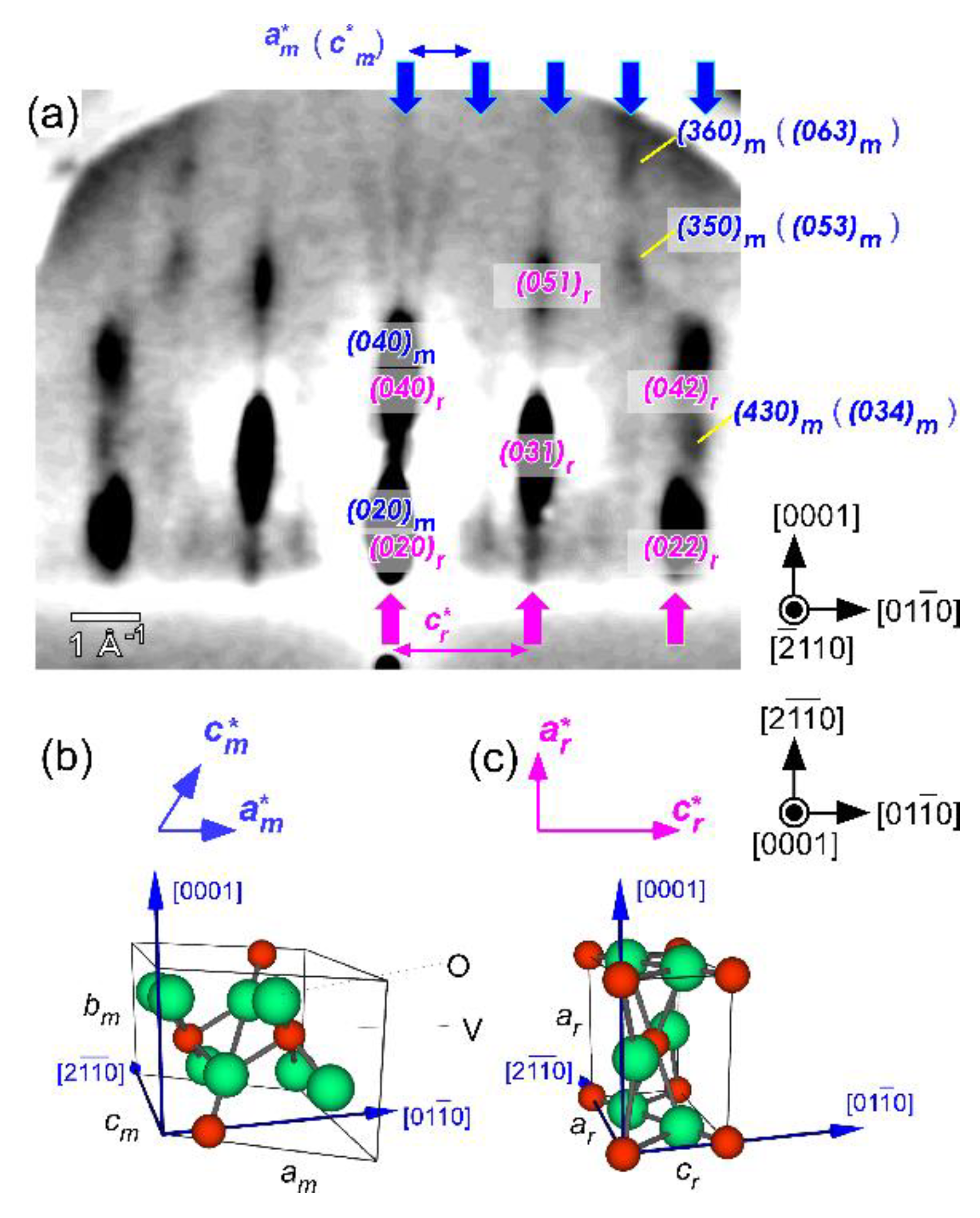
3.1. Phase-Separated VO2 Structure

XRD and RHEED results showed that an epitaxial VO2 film was grown on the Al2O3(0001) substrate. Figure 2a shows the XRD θ–2θ scan for the VO2 film at 20 °C. The strong reflections from the VO2(020) and VO2(040) planes at 2θ = 39.9° and 86.1°, respectively, indicate VO2 growth on the Al2O3(0001) substrate with its (010) plane parallel to the substrate surface [44]. Figure 2b shows the VO2(020) peak at various temperatures. With decreasing temperature from 120 °C to 20 °C, the peak position shifted toward a higher angle. The estimated lattice constant b is plotted against temperature in Figure 2c. The lattice constant b rapidly changed from 4.518 Å at 80 °C to 4.512 Å at 50 °C, that is, the thermal expansion coefficient was ~ 4 × 10 4 °C−1, while the thermal expansion coefficient was only ~ 7 × 10 6 °C−1 ( ~ 1 × 10 5 °C−1) below 50 °C (above 80 °C). This irregular thermal expansion has been established as a characteristic of the phase transition of VO2 [45]. The thermal expansion of the Al2O3 substrate in the c direction, was ~ 6 × 10 6 °C−1, as shown in the inset of Figure 2c, which is consistent with the value of 5 × 10⁻⁶ °C−1 (c direction) for the Al2O3 single crystal [46] within the experimental error. Thus, Figure 2c clearly indicates the structure transition from rutile VO2 (P42/mmm) at a high temperature to monoclinic VO2 (P21/c) at a low temperature [16]. The temperature dependence of the lattice constant indicates that during the phase transition in the cooling process, the initial state is rutile at T ≥ 90 °C, which is followed by a coexisting rutile/monoclinic state at 50 °C < T < 80 °C and a monoclinic state at T ≤ 50 °C.
RHEED patterns directly reveal the coexisting states in VO2 through the phase transition. Figure 3a shows a typical [ 2 ¯ 110 ] A l 2 O 3 -incident RHEED pattern from VO2 at 70 °C. The diffraction pattern consisted of two phases with different periodicities in the [ 01 1 ¯ 0 ] A l 2 O 3 direction. The most prominent diffraction peaks of one phase are noted by ( 020 ) r ,   ( 040 ) r ,   ( 031 ) r ,   ( 051 ) r ,   ( 022 ) r , and ( 042 ) r which are also indicated by pink arrows; these peaks have a period of 2.2 1 in the in-plane direction, which corresponds to the reciprocal lattice unit, c r * = 2 π / c r = 2.20   1 , along the c axis of the rutile VO2 phase. At a different incident azimuth angle, [ 01 1 ¯ 0 ] A l 2 O 3 -incident RHEED patterns (not shown) indicated diffraction peaks with a period of 1.4 1 corresponding to a r * = 1.38   1 . Thus, the crystalline orientation relationship of the prominent phase at higher temperatures is rutile VO2 (010)[100] Al2O3 (0001) 2 ¯ 110 (Figure 3c), as reported in Ref. [44]. The other phase had a shorter in-plane periodicity (1.3–1.4 1 ) at the [ 2 ¯ 110 ] A l 2 O 3 incidence, as shown by cyan arrows in Figure 3a. This phase is ascribed to monoclinic VO2(010)[001] (or [100]) Al2O3(0001) 2 ¯ 110 (Figure 3b) because the reciprocal lattice units, a m * = 1.30   1 and c m * = 1.39   1 , correspond to the shorter periodicity in RHEED (Figure 3a). Some diffraction peaks are noted as ( 350 ) m ,   ( 360 ) m , and ( 430 ) m (or ( 053 ) m ,   ( 063 ) m , and ( 034 ) m ). Since XRD showed monoclinic VO2[010] Al2O3[0001] (Figure 2), one can see the epitaxial VO2(010) growth on Al2O3(0001). The key point of the structural transformation between rutile and monoclinic VO2 observed in XRD and RHEED is not gradual with homogeneous changes, but comprises partial generations of drastic change from rutile to monoclinic with the spatial coexistence of the two phases, that is, phase-separated structure. This observation indicates that the gradual resistance change observed in an R-T curve (Figure 1) is associated with the propagation of the local crystallographic transformation, which is consistent with previous studies [37,47].

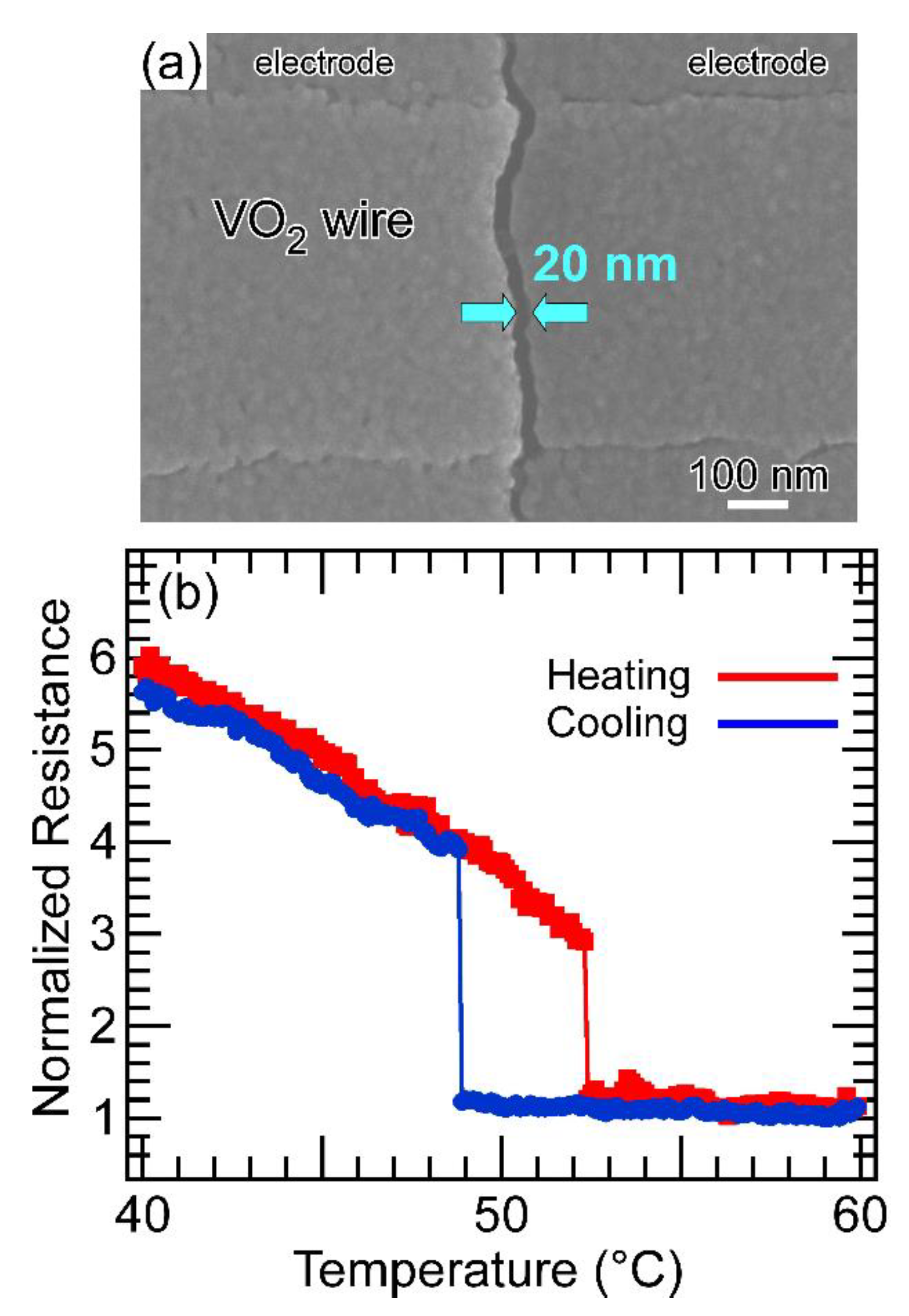
3.2. Transport Properties in the Phase-Separated VO2

For phase-separated materials, by utilizing the spatial confinement effect, it is possible to isolate individual contributions from specific interactions through their inherent length scale [35,36]. To realize the nano-confinement effect, a pair of Au/Ti electrodes with a gap length of 20 nm was attached along the length of a VO2 wire as shown in Figure 4a,b shows a typical R-T curve from the VO2 wire sample with W of 600 nm and L of 20 nm. Interestingly, one-step rapid resistivity changes were observed in both the heating and cooling processes, in contrast to the continuous changes in a macroscopic VO2 film sample (Figure 1). These one-step resistivity changes indicate the occurrence of the nano-confinement effect; the isolation of a single domain into a nano-space of 600 nm × 20 nm was realized. Although the VO2 wire sample with the nano-gap electrodes showed one-step resistance changes, their change ratio through IMT and MIT was smaller than those in the film sample, which is mainly because of the unintended damages during dry etching process. However, the one-step change which is absent in the macrosize sample clearly showed that this sample exhibit a prototype of first order transition.
VO2 undergoes a MIT and IMT accompanied by a structural transition: from a high-symmetry, metallic rutile phase at to a low-symmetry insulating monoclinic phase with V-V dimerization in cooling (MIT) process and vice versa in heating (IMT) process [2]. The IMT in VO2 is understood by the collapse of an insulating state (electron crystal) to a metallic state (electron liquid). This is a simple picture for a nano-scale single domain. The observation of the step changes in resistivity due to the spatial confinement effect shows that the single domain has an ideal first-order IMT and MIT with one-step resistivity change. Therefore, the ensemble of the step IMTs and MITs in a macrosize sample, where the IMT and MIT in numerous domains contributes to the observable IMT and MIT as an R-T curve, should show a gradual resistivity change without step changes as shown in Figure 1. Such a spatial distribution of the metal and insulator domains is illustrated in Figure 5a.
To consider the phase-separated condition quantitatively, we have proposed the statistical transition model [18,35], where the IMT and MIT property of a single domain, the number of domains ND, in the sample, and their statistical behavior, that is, the TI→M and TM→I distribution, are taken into account. The step resistivity change reflects the IMT and MIT from a single domain, showing the ideal first-order transition. Figure 5b shows the ideal R-T curve for a VO2 single domain through the IMT and MIT. For example, in the heating (cooling) process, the domain has two transport properties defined as RIns(T) and RMet(T); RIns(T) switches with RMet(T) at TI→M (RMet(T) switches with RIns(T) at TM→I). Therefore, assuming the simplest first-order IMT and MIT, the resistivity of a single domain Rs(T) is described as
R s ( T ) = { R I n s ( T ) = A T e x p ( E g k B T )                                 ( T > T M I : i n s u l a t i n g   r e g i o n ) R M e t ( T ) = R 0 + B T 2 + C T 5                             ( T T M I : m e t a l l i c   r e g i o n ) ,
where R I n s ( T ) R M e t ( T ) . A, B, and C are coefficients, R0 is the residual resistivity in the metallic phase, Eg is the activation energy in the insulating (semiconducting-like) phase, and kB is the Boltzmann constant. The parameters in Equation (2) were obtained by fitting for an R-T curve for a film sample.
In the temperature-induced IMT of VO2, metal domains initially nucleate at seed sites in a sample, then grow and spread with increasing temperature. The domain dynamics, i.e., the temperature-dependent population of the metal domains, strongly affects the observable transport property of the sample. To express the phase-separated condition as domain dynamics, the TI→M and TM→I distribution is defined in this model. The direct observation of the coexistence of metal and insulator domains in the vicinity of the observable TI→M and TM→I [13,14,15,16,17,18,19,20,21,22,23,24,25] indicates that the TI→M and TM→I values of the single domains are distributed. The distribution of TI→M and TM→I for each domain can be described using the Gaussian function as
f ( T ) = 1 2 π σ 2 e x p [ ( T T c e n t e r ) 2 2 σ 2 ] ,
where σ is the half width of the Gaussian distribution and Tcenter is the temperature where the population of metal domains, PMet is equal to that of insulator domains, PIns, i.e., PMet(Tcenter) = PIns(Tcenter) = 50%. f(T) gives the probability of the IMT and MIT at a certain temperature. Here, the values of σ and Tcenter in the heating process are treated to be different from those in the cooling process [48]. Thus, the metal population is obtained as
P M e t ( T ) = N D · f ( T ) = 1 P I n s ( T ) .
Here, we treat the resistor network with the edge resistor having the single domain resistivity R s ( T ) in Equation (2) under Equations (3) and (4), and obtain R s a m p l e ( T ) from the cycle current equation in Equation (1).
Three-dimensional (3D) cubic-lattice networks are treated for films thicker than a metal and insulator domain size; the domain size in a VO2 film on an Al2O3 substrate was reported to be ~100 nm [17]. Since the thickness of the VO2 samples in this study was 50 nm, we can treat a 2D square-lattice network with the number of the domains ND = NL × NW × NH (= 1). Figure 5c shows a comparison between the observed and simulated R-T curves for the VO2 film. Here, the resistivity was calculated from Equations (1)–(4) assuming NL = NW = 100. The dashed curves in Figure 5c showed the good fitting of the results with this model, where the TI→M (TM→I) distribution as shown in Figure 5d (Figure 5e) was obtained. The good agreement between the experimental and simulation results indicates the validity of this model. This means that the observable R-T property of VO2 is determined by three elements: the resistivity of a single domain Rs(T), the TI→M and TM→I distributions, and the ND of the sample. It was reported that the MIT and IMT characteristics including the width of the hysteresis loop in a R-T curve depend on various structural parameters, such as external and internal stresses, grain size in a VO2 sample since the phase transition in VO2 is coupled to the defect concentration and the types of crystal defects [37,38,47]. Therefore, Rs(T) and the TI→M and TM→I distributions are characteristics of an individual samples that depend on its growth conditions. On the other hand, we can tune ND by controlling the sample size. The step resistivity changes shown in Figure 4b have been observed due to the nano-confinement effects not only in VO2 but also in other CEMs [13,18,26,35]. The minimization of the sample size results in the step resistivity change at the stochastic TI→M and TM→I corresponding to the reduction in ND. The observed TI→M (TM→I) of 52 °C (49 °C) for the VO2 wire sample with W of 600 nm and L of 20 nm (Figure 4b) was lower than that of 77 °C (65 °C) for the film sample (Figure 1). The statistical model shows that TI→M (TM→I) were distributed within a range of 50 to 100 °C (40 to 90 °C) as shown in Figure 5d (Figure 5e). The stochastic selection of a single domain as a result of the spatial confinement determined the TI→M and TM→I for the 20 nm-gap wire sample while TI→M (TM→I) is defined as a temperature at PMet (PIns)~0.6 for the macrosize sample with a high ND. The isolation of one or a few domains into the nanospace makes it possible to investigate the potentially hidden domain behavior in a macrosize sample with a high ND. Thus, the correlation between the domain size and the TI→M and TM→I distribution in the spatially confined structure was examined.

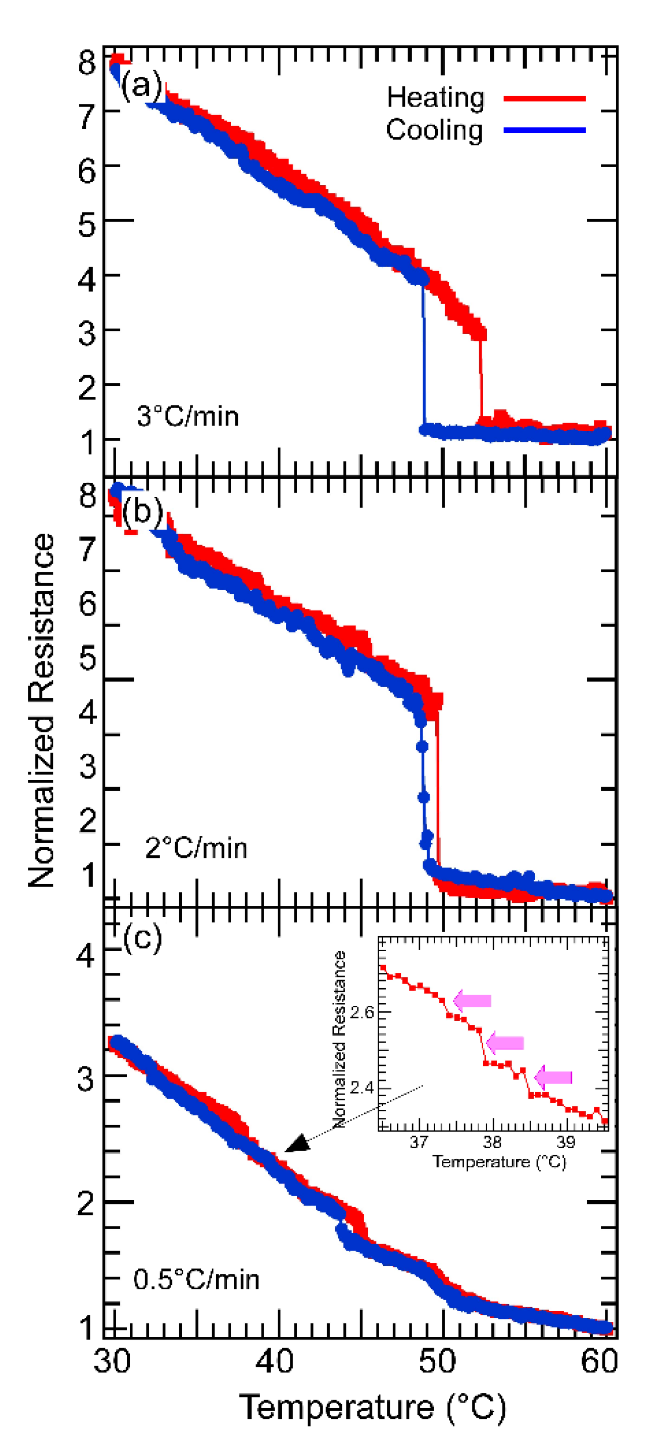
3.3. Domain Dynamics of VO2 Domains: The Effect of the Temperature-Sweep-Rate

Figure 6 shows R-T curves for the VO2 sample with different temperature-sweep-rate with W of 0.6 μm and L of 20 nm. We can see the variation of the transition behavior with the temperature-sweep-rate. At the high temperature-sweep-rate of 3 °C/min, the R-T curve showed one-step resistivity changes in both the cooling and heating processes, indicating that ND = 1 during the IMT and MIT. Interestingly, at the temperature-sweep-rate of 2 °C/min (Figure 6b), multi-step resistivity changes, that is, multiple points in the transient stage in the cooling process, were observed while the one-step resistivity change was maintained in the heating process. The R-T curves at the temperature-sweep-rate of 0.5 °C/min consisted of the many small step changes, as shown in the insets (Figure 6c). These results clearly showed that reducing of the temperature-sweep-rate induced the multi-step resistivity changes. The change from one-step to multi-step resistivity changes indicates an increase in the ND of the sample, i.e., a decrease in domain size. Our observed tendency is consistent with previous reports. Lopez et al. reported the effect of sample size on TI→M and TM→I for VO2 nanoparticles [41], where an increase (decrease) in TI→M (TM→I) with sample miniaturization was observed. They considered that the size dependence is associated with the nucleation statistics where the density of nucleating defects is a power function of the driving force for the MIT and IMT. Yoon et al. found an effect of size on the phase transition speed [39]; the transition speed was roughly proportional to 1/w, where w is the width of the VO2 microcrystal. They pointed out the possibility of size-dependent thermal dissipation. Oike et al. reported size-dependent supercooling phenomena in strongly correlated electron systems and suggested a nucleation mechanism [40]. In general, systematic shifts of TI→M (TM→I) toward high (low) temperatures when increasing temperature-sweep-rate are observed, implying that nucleation events are involved in the first-order transition [49]. Namely, the nucleation rate of the electronic domains is consistent with the generation speed of the operational defects in the sample [38,40,47]. Thus, we can expect the phenomena based on the nucleation mechanism [40]. Most first-order phase transitions are initiated by nucleation, which is a critical rate event. The first-order transition could be kinetically suppressed under sufficient rapid cooling or heating; the nucleation growth rate of the domains leading to the first-order transitions is slow compared with the external temperature-sweep-rate. The most extensively studied realization of this scenario is classical liquids [50]. Extension of this manner will be applicable for the IMT and MIT in VO2.
In the frame of this phase-separated scenario, an increase of the transition (nucleation) sites is described as an increase in ND with decreasing the mean domain size: Dave under the slow temperature-sweep-rate. The nucleation of metal and insulator domains in heating and cooling processes, i.e., insulator-metal and metal-insulator transitions, respectively, occurs preferentially at defect sites, such as grain boundaries, surfaces, impurity atoms, vacancies, and dislocations. Since the probability of IMT and MIT depends on the availability of a suitable nucleating defect in the sample space, a rapid temperature sweep, and/or minimization of the sample volume causes a kinetic avoidance of the first-order transition. Naturally, the defects would have preferentially interact with an embryo of a growing metal/insulator domain in order to overcome an activation barrier toward nucleation. During a temperature sweep, the phase-transition kinetics competes with the experimental temperature-sweep-rate. In VO2, the transition is mainly driven by phonons in addition to a contribution from electrons [51]. When the temperature-sweep-rate exceeds the phase-transition kinetics, the thermal dynamic motions of V and O atoms leading multiple nucleation at latent defect cites are suppressed, and eventually a transition occurs at an energetically preferential defect site. On the other hand, when the temperature-sweep-rate is sufficiently low, the phase transition is fully completed even at latent defect sites.
The nucleation rate dependency and corresponding resistivity behavior have been observed as the size effects in the phase transition. In the phase transition of VO2, the size effects have been typically reported for nano-particle systems; these effects originate from size-dependent thermal dissipation [39,41,52,53,54,55]. The decreasing domain size consequently induces the shifts of TI→M and TM→I. An increase in the rate of effective thermal exchange in the nano-scale sample leads to a lower (higher) TI→M (TM→I). Additionally, the increase in hysteresis width in the R-T curve for a sample consisting of smaller nano-particles [41] implies that a wider TI→M and TM→I distribution corresponds to a larger numbers of available defect sites in the sample. The temperature-sweep-rate dependent behavior of the step changes in resistivity in the nano-confined VO2 sample (Figure 6) clearly reveals the increases in ND and TI→M and TM→I variation in addition to the shift of Tcenter.
The statistical transition model based on the observed results for a spatially confined sample can adequately explain and seamlessly assign the complex domain dynamics in phase-separated VO2 from the micro-scale to the macro-scale. When the sample size increases from the micro-scale (~Dave) to the macro-scale (>>Dave), the ND of the sample drastically increases. For example, ND was estimated to be a few hundreds in a 2 × 2 μm2 VO2 sample (W = 2 μm and L = 2 μm). This sample showed a gradual R-T curve without any step changes, which means that the contribution of each domain is buried and is not detectable in larger sample. Actually, we observed the temperature-sweep-rate dependence as a slight temperature shift. In this sample, TI→M reduction was confirmed, while TM→I was insensitive to the temperature-sweep-rate, which reflects the structural stability of VO2 phases. The low-temperature monoclinic phase is energetically favored over the high-temperature rutile phase [49], and the MIT requires a larger driving forces than the IMT in order to overcome the nucleation barrier in VO2 [41]. TI→M was reduced to 2–3 °C in the 2 × 2 μm2 VO2 sample when the temperature-sweep-rate was changed from 3 °C/min to 0.5 °C/min. According to the IMT statistical model with a random resistor network, the TI→M increase of 2–3 °C was ascribed to the 20–100-fold increase in ND under a constant Tcenter. The TI→M increase may be cause by the decrease of PC. It was reported the critical fraction value: PC depends on the ND and arrangement of the metallic (insulating) domains in a sample [26,27]. That means the degree of the changing ratio, i.e., the shape of the R-T curve (one-step, multi-steps, and gradual changes) depends on the ND; the changing ratio and sharpness is enhanced with decreasing ND. Additionally, the decrease of ND enhances the contribution of each single domain to the total change in the R-T curve. Therefore, the 20–100-fold increase in ND caused the corresponding ~4–10-fold reduction in domain size associated with the 2–3 °C increase in TI→M, which is consistent with previous studies [41,53].

4. Conclusions

The domain dynamics in phase-separated VO2 was systematically studied. To identify the single-domain IMT and MIT behavior, a spatially confined VO2 sample was prepared. The step changes in the resistivity of a nano-confined sample, which are absent in macrosize VO2 samples, correspond to the first-order IMT and IMT from a single domain and the distributed TI→M and TM→I. Changing the temperature-sweep-rate led to the variation of the transition behavior corresponding to nucleation events. As a result of the competition between the phase-transition kinetics and the experimental temperature-sweep-rate, a realistic domain size and their TI→M and TM→I were decided. We proposed a statistical transition model, where the macroscopic transition behavior, i.e., an observable R-T, was reproduced using the one-step R-T curve for a single domain, the total number of domains in the sample, and their TI→M and TM→I distribution. In the frame of the statistical transition model, the phase-separation scenario and temperature-sweep-rate-dependent behavior were able to be explained quantitatively. The advantage of studying a nano-confined sample is the quantification of the domain generation (nucleation) process. The number of the step changes in an R-T curve and their temperature distribution indicate ND and TI→M and TM→I distribution. Direct understanding of the statistical IMT and MIT properties of electronic domains in the nano-confined sample can advance the detailed physics of phase transition. Furthermore, the number of domains can be controlled by designing the sample structure, i.e., confinement effect. The arbitrary control of ND and TI→M and TM→I temperature distribution would lead to a preferential response, which can be a good guideline for realizing the functional nanoelectronic devices based on the phase-separated CEMs.

Author Contributions

Conceptualization, A.N.H. and H.T.; sample fabrication, A.N.H., A.I.O., and Y.N.; data curation, A.N.H., A.I.O., and K.H.; writing—original draft preparation, A.N.H.; writing—review and editing, A.I.O., K.H., Y.N., H.S., H.A., and H.T.; scientific discussion and project administration, A.N.H.; funding acquisition, A.N.H. and H.T.; All authors have read and agreed to the published version of the manuscript.

Funding

This research was funded by JSPS KAKENHI (Scientific Research B (Nos. 18H01871 and 20H02483), Scientific Research A (No. 17H01054), and Grant-in-aid for Young Scientists (20K15116)), A-STEP from JST (No. JPMJTM19CM) and by the Dynamic Alliance for Open Innovation Bridging Human, Environment and Materials of the Network Joint Research Center for Materials and Devices (Nos. 2015352 and 20203017), Kansai Research Foundation for Technology Promotion, TEPCO Memorial Foundation, SEI Group CSR Foundation, Futaba Research Grant Program of the Futaba Electronics Memorial Foundation.

Acknowledgments

The authors thank Saeko Tonda and Shouichi Sakakihara (ISIR, Osaka Univ.) for their helpful support for the sample preparation. The authors also thank Shouhei Katao (NAIST) for his assistance in XRD measurements. This work was also partly supported by the Nanotechnology Platform Projects (Nanotechnology Open Facilities in Osaka University, and Synthesis of Molecules and Materials in NAIST) of MEXT, Japan (Grant Nos. JPMXP09F20OS0008 and JPMXP09S20OS0006).

Conflicts of Interest

The authors declare no conflict of interest.

References and Note

  1. Morin, E.J. Oxides Which Show a Metal-to-Insulator Transition at the Neel Temperature. Phys. Rev. Lett. 1959, 3, 34. [Google Scholar] [CrossRef]
  2. Eyert, V. The metal-insulator transitions of VO2: A band theoretical approach. Ann. Phys. 2002, 11, 650–702. [Google Scholar] [CrossRef] [Green Version]
  3. Yang, Z.; Ko, C.; Ramanathan, S. Oxide Electronics Utilizing Ultrafast Metal-Insulator Transitions. Annu. Rev. Mater. Res. 2011, 41, 337–367. [Google Scholar] [CrossRef]
  4. Cavalleri, A.; Tóth, C.; Siders, C.W.; Squier, J.A.; Raksi, F.; Forget, P.; Kieffer, J.C. Femtosecond Structural Dynamics in VO2 during an Ultrafast Solid-Solid Phase Transition. Phys. Rev. Lett. 2001, 87, 237401. [Google Scholar] [CrossRef] [PubMed] [Green Version]
  5. Kübler, C.; Ehrke, H.; Huber, R.; Lopez, R.; Halabica, A.; Haglund, R.F.; Leitenstorfer, A. Coherent Structural Dynamics and Electronic Correlations during an Ultrafast Insulator-to-Metal Phase Transition in VO2. Phys. Rev. Lett. 2007, 99, 116401. [Google Scholar] [CrossRef]
  6. Kim, H.-T.; Chae, B.-G.; Youn, D.-H.; Maeng, S.-L.; Kim, G.; Kang, K.-Y.; Lim, Y.-S. Mechanism and Observation of Mott Transition in VO2-Based Two- and Three-Terminal Devices. New J. Phys. 2004, 6, 52. [Google Scholar] [CrossRef] [Green Version]
  7. Stefanovich, G.; Pergament, A.; Stefanovich, D. Electronical Switching and Mott Transition in VO2. J. Phys. Condens. Matter 2000, 12, 8837–8845. [Google Scholar] [CrossRef]
  8. Strelcov, E.; Lilach, Y.; Kolmakov, A. Gas Sensor Based on Metal-Insulator Transition in VO2 Nanowire Thermistor. Nano Lett. 2009, 9, 2322–2326. [Google Scholar] [CrossRef]
  9. Yajima, T.; Nishimura, T.; Toriumi, T. Positive-bias gate-controlled metal–insulator transition in ultrathin VO2 channels with TiO2 gate dielectronics. Nat. Commun. 2015, 6, 1–9. [Google Scholar] [CrossRef]
  10. Pellegrino, L.; Manca, N.; Kanki, T.; Tanaka, H.; Biasotti, M.; Bellingeri, E.; Siri, A.S.; Multistate, D. Multistate Memory Devices Based on Free-Standing VO2/TiO2 Microstructures Driven by Joule Self-Heating. Adv. Mater. 2012, 24, 2929–2934. [Google Scholar] [CrossRef]
  11. Shukla, N.; Thathachary, A.V.; Agrawal, A.; Paik, H.; Aziz, A.; Schlopp, D.G.; Gupta, S.K.; Engel-Herbert, R.; Datta, S. A Steep-Slope Transistor Based on Abrupt Electronic Phase Transition. Nat. Commun. 2015, 6, 1–6. [Google Scholar] [CrossRef] [PubMed] [Green Version]
  12. IEEE. The International Roadmap for Devices and Systems. 2020. Available online: https://irds.ieee.org/ (accessed on 7 July 2020).
  13. Tsuji, Y.; Kanki, T.; Murakami, Y.; Tanaka, H. Single-step metal-insulator transition in thin film-based vanadium dioxide nanowires with a 20 nm electrode gap. Appl. Phys. Express 2019, 12, 025003. [Google Scholar] [CrossRef]
  14. Ueda, H.; Kanki, T.; Tanaka, H. Manipulation of metal-insulator transition characteristics in aspect ratio-controlled VO2 micro-scale thin films on TiO2 (001) substrates. Appl. Phys. Lett. 2013, 102, 153106. [Google Scholar] [CrossRef]
  15. Qazilbash, M.M.; Brehm, M.; Chae, B.G.; Ho, P.C.; Andreev, G.O.; Kim, B.J.; Yun, S.J.; Balatsky, A.V.; Maple, M.B.; Keilmann, F.; et al. Mott Transition in VO2 Revealed by Infrared Spectroscopy and Nano-Imaging. Science 2007, 318, 1750–1753. [Google Scholar] [CrossRef] [Green Version]
  16. He, X.; Xu, T.; Xu, X.; Zeng, Y.; Xu, J.; Sun, L.; Wang, C.; Xing, H.; Wu, B.; Lu, A.; et al. In Situ Atom Scale Visualization of Domain Wall Dynamics in VO2 Insulator-Metal Phase Transition. Sci. Rep. 2015, 4, 6544. [Google Scholar] [CrossRef] [Green Version]
  17. Takami, H.; Kawatani, K.; Ueda, H.; Fujiwara, K.; Kanki, T.; Tanaka, H. Tuning metal-insulator transition by one dimensional alignment of giant electronic domains in artificially size-controlled epitaxial VO2 wires. Appl. Phys. Lett. 2012, 101, 263111. [Google Scholar] [CrossRef]
  18. Tsubota, S.; Hattori, A.N.; Nakamura, T.; Azuma, Y.; Majima, Y.; Tanaka, H. Enhancement of discrete changes in resistivity in engineered VO2 heterointerface nanowall wire. Appl. Phys. Express 2017, 10, 115001. [Google Scholar] [CrossRef]
  19. Kawatani, K.; Kanki, T.; Tanaka, H. Formation mechanism of a microscale domain and effect on transport properties in strained VO2 thin films on TiO2 (001). Phys. Rev. B 2014, 90, 054203. [Google Scholar] [CrossRef]
  20. Kawatani, K.; Takami, H.; Kanki, T.; Tanaka, H. Metal-insulator transition with multiple micro-scaled avalanches in VO2 thin film on TiO2 (001) substrates. Appl. Phys. Lett. 2012, 100, 173112. [Google Scholar] [CrossRef]
  21. Wu, J.; Gu, Q.; Guiton, B.S.; Leom, N.P.; Ouyang, L.; Park, H. Strain-Induced Self Organization of Metal-Insulator Domains in Single-Crystalline VO2 Nanobeams. Nano Lett. 2006, 6, 2313–2317. [Google Scholar] [CrossRef]
  22. Wu, J.; Gu, Q.; Guiton, B.S.; Leon, N.P.; Ouyang, L.; Park, H. Surface-Stress-Induced Mott Transition and Nature of Associated Spatial Phase Transition in Single Crystalline VO2 Nanowires. Nano Lett. 2009, 9, 3392–3397. [Google Scholar]
  23. Zhang, S.; Chou, J.Y.; Lauhon, L.J. Direct Correlation of Structural Domain Formation with the Metal Insulator Transition in a VO2 Nanobeam. Nano Lett. 2009, 9, 4527–4532. [Google Scholar] [CrossRef] [PubMed]
  24. Cao, J.; Ertekin, E.; Srinivasan, V.; Fan, W.; Huang, S.; Zheng, H.; Yim, J.W.L.; Khanal, D.R.; Ogletree, D.F.; Grossman, J.C.; et al. Strain engineering and one-dimensional organization of metal–insulator domains in single-crystal vanadium dioxide beams. Nat. Nanotechnol. 2009, 4, 732–737. [Google Scholar] [CrossRef] [PubMed]
  25. Cao, J.; Fan, W.; Zheng, H.; Wu, J. Thermoelectronic Effect across the Metal−Insulator Domain Walls in VO2 Microbeams. Nano Lett. 2009, 9, 4001–4006. [Google Scholar] [CrossRef] [PubMed]
  26. Tanaka, H.; Takami, H.; Kanki, T.; Hattori, A.N.; Fujiwara, K. Artificial three dimensional oxide nanostructures for high performance correlated oxide nanoelectronics. Jpn. J. Appl. Phys. 2014, 53, 05FA10. [Google Scholar] [CrossRef]
  27. Kanki, T.; Kawatani, K.; Takami, H.; Tanaka, H. Direct observation of giant metallic domain evolution driven by electric bias in VO2 thin films on TiO2 (001) substrate. Appl. Phys. Lett. 2012, 101, 243118. [Google Scholar] [CrossRef]
  28. Sohn, A.; Kanki, T.; Sakai, K.; Tanaka, H.; Kim, D.-W. Fractal Nature of Metallic and Insulating Domain Configurations in a VO2 Thin Film Revealed by Kelvin Probe Force Microscopy. Sci. Rep. 2015, 5, 10417. [Google Scholar] [CrossRef]
  29. Dagotto, E.; Hotta, T.; Moreo, A. Colossal magnetoresistant materials: The key role of phase separation. Phys. Rep. 2001, 344, 1–153. [Google Scholar] [CrossRef] [Green Version]
  30. Uehara, M.; Mori, S.; Chen, C.H.; Cheong, S.-W. Percolative phase separation underlies colossal magnetoresistance in mixed-valent manganites. Nature 1999, 399, 560–563. [Google Scholar] [CrossRef]
  31. Ward, T.Z.; Liang, S.; Fuchigami, K.; Yin, L.F.; Dagotto, E.; Plummer, E.W.; Shen, J. Reemergent Metal-Insulator Transitions in Manganites Exposed with Spatial Confinement. Phys. Rev. Lett. 2008, 100, 247204. [Google Scholar] [CrossRef]
  32. Preziosi, D.; Lopez-Mir, L.; Li, X.; Cornelissen, T.; Lee, J.H.; Trier, F.; Bouzehouane, K.; Valencia, S.; Gloter, A.; Barthélémy, A.; et al. Direct Mapping of Phase Separation across the Metal-Insulator Transition of NdNiO3. Nano Lett. 2018, 18, 2226–2232. [Google Scholar] [CrossRef] [PubMed]
  33. Mattoni, G.; Zubko, P.; Maccherozzi, F.; Torren, A.J.H.; Boltje, D.B.; Hadjimichael, M.; Manca1, N.; Catalano, S.; Gibert, M.; Liu, Y.; et al. Striped nanoscale phase separation at the metal-insulator transition of heteroepitaxial nickelates. Nat. Commun. 2016, 93, 1–7. [Google Scholar] [CrossRef] [PubMed] [Green Version]
  34. Lee, J.H.; Trier, F.; Cornelissen, T.; Preziosi, D.; Bouzehouane, K.; Fusil, S.; Valencia, S.; Bibes, M. Imaging and Harnessing Percolation at the Metal–Insulator Transition of NdNiO3 Nanogaps. Nano Lett. 2019, 19, 7801–7805. [Google Scholar] [CrossRef] [PubMed]
  35. Hattori, A.N.; Fujiwara, Y.; Fujiwara, K.; Nguyen, T.V.A.; Nakamura, T.; Ichimiya, M.; Ashida, M.; Tanaka, H. Identification of Giant Mott Phase Transition of Single Electronic Nanodomain in Manganite nanowall wire. Nano Lett. 2015, 15, 4322–4328. [Google Scholar] [CrossRef] [PubMed]
  36. Rakshit, R.; Hattori, A.N.; Naitoh, Y.; Shima, H.; Akinaga, H.; Tanaka, H. Three-dimensional Nanoconfinement Supports Verwey Transition in Fe3O4 Nanowire at 10 nm length scale. Nano Lett. 2019, 19, 5003–5010. [Google Scholar] [CrossRef]
  37. Fan, W.; Cao, J.; Seidel, J.; Gu, Y.; Yim, J.W.; Barrett, C.; Yu, K.M.; Ji, J.; Ramesh, R.; Chen, L.Q.; et al. Large kinetic asymmetry in the metal-insulator transition nucleated at localized and extended defects. Phys. Rev. B 2011, 83, 235102. [Google Scholar] [CrossRef] [Green Version]
  38. Wei, J.; Wang, Z.; Chen, W.; Cobden, D.H. New aspects of the metal-insulator transition in single-domain vanadium dioxide nanobeams. Nat. Nanotechnol. 2009, 4, 420–424. [Google Scholar] [CrossRef] [Green Version]
  39. Yoon, J.; Kim, H.; Chen, X.; Tamura, N.; Mun, B.S.; Park, C.; Ju, H. Controlling the Temperature and Speed of the Phase Transition of VO2 Microcrystals. ACS Appl. Mater. Interfaces 2016, 8, 2280–2286. [Google Scholar] [CrossRef] [Green Version]
  40. Oike, H.; Suda, M.; Kamitani, M.; Ueda, A.; Mori, H.; Tokura, Y.; Yamamoto, H.M.; Kagawa, F. Size effects on supercooling phenomena in strongly correlated electron systems: IrTe2 and θ−(BEDT−TTF)2 RbZn (SCN)4. Phys. Rev. B 2018, 97, 085102. [Google Scholar] [CrossRef] [Green Version]
  41. Lopez, R.; Haynes, T.E.; Boatner, L.A. Size effects in the structural phase transition of VO2 nanoparticles. Phys. Rev. B 2002, 65, 224113. [Google Scholar] [CrossRef]
  42. Naitoh, Y.; Tsukagoshi, K.; Murata, K.; Mizutani, W. A Reliable Method for Fabricating sub-10 nm Gap Junctions Without Using Electron Beam Lithography. E-J. Surf. Sci. Nanotechnol. 2003, 1, 41–44. [Google Scholar] [CrossRef] [Green Version]
  43. Bollobas, B. Modern Graph Theory (Graduate Texts in Mathematics); Springer: Berlin, Germany, 1998. [Google Scholar]
  44. Okimura, K.; Sakai, J. Changes in Lattice Parameters of VO2 Films Grown on c-Plane Al2O3 Substrates across Metal–Insulator Transition. Jpn. J. Appl. Phys. 2009, 48, 045504. [Google Scholar] [CrossRef]
  45. Kawakubo, T.; Nakagawa, T. Phase Transition in VO2. J. Phys. Soc. Jpn. 1964, 19, 517–519. [Google Scholar] [CrossRef]
  46. Peggs, I.P. Thermal Expansion 6; Plenum Press: New York, NY, USA, 1978; pp. 191–201. [Google Scholar]
  47. Yang, Y.; Lee, K.; Zobel, M.; Maćković, M.; Unruh, T.; Spiecker, E.; Schmuki, P. Formation of Highly Ordered VO2 Nanotubular/Nanoporous Layers and Their Supercooling Effect in Phase Transitions. Adv. Mater. 2012, 24, 1571–1575. [Google Scholar] [CrossRef] [PubMed]
  48. In the simulation in Figs. 5(c–e), = 8 °C, Tcenter = 77 °C in heating (IMT) process and = 9 °C, Tcenter = 65 °C in the cooling (MIT) process were used.
  49. Kagawa, F.; Oike, H. Quenching of Charge and Spin Degrees of Freedom in Condensed Matter. Adv. Mater. 2017, 29, 1601979. [Google Scholar] [CrossRef]
  50. Debenedetti, P.G.; Stillinger, F.H. Supercooled liquids and the glass transition. Nature 2001, 410, 259–267. [Google Scholar] [CrossRef]
  51. Mellan, T.A.; Wang, H.; Schwingenschlögl, U.; Crau-Crespo, R. Origin of the transition entropy in vanadium dioxide. Phys. Rev. B 2019, 99, 064113. [Google Scholar] [CrossRef] [Green Version]
  52. Wang, M.; Xue, Y.; Cui, Z.; Zhang, R. Size-Dependent Crystal Transition Thermodynamics of Nano-VO2 (M). J. Phys. Chem. C 2018, 122, 8621–8627. [Google Scholar] [CrossRef]
  53. Whittaker, L.; Jaye, C.; Fu, Z.; Fischer, D.A.; Banerjee, S. Depressed Phase Transition in Solution-Grown VO2 Nanostructure. J. Am. Chem. Soc. 2009, 131, 8884–8894. [Google Scholar] [CrossRef]
  54. Chena, S.; Ma, H.; Dai, J.; Yi, X. Nanostructured vanadium dioxide thin films with low phase transition temperature. Appl. Phys. Lett. 2007, 90, 101117. [Google Scholar] [CrossRef]
  55. Dai, L.; Cao, C.; Gao, Y.; Luo, H. Synthesis and phase transition behavior of undoped VO2 with a strong nano-size effect. Sol. Energy Mater. Sol. Cells 2011, 95, 712–715. [Google Scholar] [CrossRef]
Figure 1. Temperature dependent resistivity curve for epitaxial VO2 film grown on Al2O3(0001). Drastic changes in resistivity corresponding to the insulator-metal transition (IMT) and metal-insulator transition (MIT) occurs at ~77 °C and ~65 °C in the heating (red line) and cooling (blue line) processes, respectively.
Crystals 10 00631 g001
Figure 2. (a) XRD θ–2θ scan for VO2 film on Al2O3(0001) substrate at 20 °C. (b) VO2(020) diffraction peak at various temperatures. (c) Temperature-dependent lattice constant b of the VO2 film. The inset shows the lattice constant c of Al2O3, which monotonically increases with temperature. A small peak at ~75° in (a) corresponds to Ni alloys in the sample holder.
Crystals 10 00631 g002
Figure 3. (a) Typical reflection high-energy electron diffraction (RHEED) pattern of VO2 film observed at 70 °C. The incident electron beam direction was [ 2 ¯ 110 ] A l 2 O 3 . The spots indicated by blue and pink reflections (and arrows) correspond to the monoclinic and rutile VO2 phases, respectively. Schematic two-dimensional (2D) reciprocal lattice unit vectors on ( 0001 ) A l 2 O 3 (top panel) and real-space crystal structures (bottom panel) for (b) monoclinic and (c) rutile VO2 phases. The crystalline orientation relationships of monoclinic and rutile VO2(010) to Al2O3(0001) are visualized with blue arrows representing Al2O3 [ 01 1 ¯ 0 ] ,   [ 2 ¯ 110 ] ,   and   [ 0001 ] .
Crystals 10 00631 g003
Figure 4. (a) Typical SEM image of VO2 wire with width of 600 nm after depositing a pair of Au/Ti electrodes. The gap distance of the electrodes was 20 nm, which corresponds to the VO2 region for the electronic resistivity measurement. (b) Normalized R-T curve for the VO2 wire with 20 nm-gap electrodes. One-step changes in resistivity were observed in both the heating (red) and cooling (blue) processes. The resistivity was normalized by the value at 60 °C. The temperature-sweep-rate was 3.0 °C/min.
Crystals 10 00631 g004
Figure 5. (a) Schematic of the phase-separated VO2 with (NL × NW) domain geometry: metal (pink) and insulator (cyan) phases coexist between the electrodes. (b) Ideal R-T curves through the IMT and MIT for a single domain with TI→M of 70 °C and TM→I of 60 °C, respectively. (c) Comparison between the observed R-T curve for the VO2 sample (solid lines) and the simulated one using Equation (1) (dashed line). Estimated ND values in (d) IMT and (e) MIT processes with TI→M = 77 °C and TM→I = 65 °C, respectively.
Crystals 10 00631 g005
Figure 6. Normalized R-T curves for the VO2 wire with 20 nm-gap-electrodes measured at temperature-sweep-rates of (a) 3 °C/min, (b) 2 °C/min, and (c) 0.5 °C/min. Magnified step changes (indicated by arrows) are shown in the insets of (c).
Crystals 10 00631 g006

